Fairchild Semiconductor MM74HCT574WMX, MM74HCT574SJ, MM74HCT574SJX, MM74HCT574MTCX, MM74HCT574CW Datasheet
...
February 1990
Revised May 1999
MM74HCT573 • MM74HCT574 Octal D-Type Latch • 3-STATE Octal D-Type Flip-Flop
© 1999 Fairchild Semiconductor Corporation DS010627.prf www.fairchildsemi.com
MM74HCT573 • MM74HCT574
Octal D-Type Latch • 3-STATE Octal D-Type Flip-Flop
General Description
The MM74HCT573 octal D-type latches and
MM74HCT574 octal D-type flip-flop advanced silicon-gate
CMOS technology, which provides the inherent benefits of
low power consumption and w ide power su pply range, but
are LS-TTL input and output characteristic and pin-out
compatible. The 3-STATE outputs are capable of driving 15
LS-TTL loads. All inputs are protected from damage due to
static discharge by internal diodes to V
CC
and ground.
When the MM74HCT573 Latch Enable in put is HIGH, the
Q outputs will follow the D inputs. When the Latch Enable
goes LOW, data at the D inputs will be retained at the outputs until Latch Enable retu rns HIGH again. When a high
logic level is applied to the Output Control input, all outputs
go to a high impedan ce state, regardless of wha t signals
are present at the other inputs and the state of the storage
elements.
The MM74HCT574 a re positive edge triggered flip-fl ops.
Data at the D inputs, meeting the setup and hold time
requirements, are transferred to the Q outputs on positive
going transitions of the Clock (CK) input. When a high logic
level is applied to the Output Control (OC) input, all outputs
go to a high impeda nce state, regardless of wh at signals
are present at t he other inputs and the sta t e of th e s t or age
elements.
The MM74HCT devi ces are intended to inter face bet ween
TTL and NMOS components and standard CMOS devices.
These parts are also plug in replacements for LS-TTL
devices and can be used to reduce pow er consumption in
existing designs.
Features
■ TTL input characteristic compatible
■ Typical propagation delay: 18 ns
■ Low input current: 1 µA maximum
■ Low quiescent current: 80 µA maximum
■ Compatible with bus-oriented systems
■ Output drive capability: 15 LS-TTL loads
Ordering Codes:
Devices also availab le in Tape and Reel. Specify by appending su ffix let te r “X” to the ordering code .
Order Number Package Number Package Description
MM74HCT573WM M20B 20-Lead Small Outline Integrated Circuit (SOIC), JEDEC MS-013, 0.300 Wide
MM74HCT573SJ M20D 20-Lead Small Outline Package (SOP), EIAJ TYPE II, 5.3mm Wide
MM74HCT573MTC MTC20 20-Lead Thin Shrink Small Outline Package (TSSOP), JEDEC MO-153, 4.4mm Wide
MM74HCT573N N20A 20-Lead Plastic Dual-In-Line Package (PDIP), JEDEC MS-001, 0.300 Wide
MM74HCT574WM M20B 20-Lead Small Outline Integrated Circuit (SOIC), JEDEC MS-013, 0.300 Wide
MM74HCT574SJ M20D 20-Lead Small Outline Package (SOP), EIAJ TYPE II, 5.3mm Wide
MM74HCT574MTC MTC20 20-Lead Thin Shrink Small Outline Package (TSSOP), JEDEC MO-153, 4.4mm Wide
MM74HCT574N N20A 20-Lead Plastic Dual-In-Line Package (PDIP), JEDEC MS-001, 0.300 Wide

www.fairchildsemi.com 2
MM74HCT573 • MM74HCT574
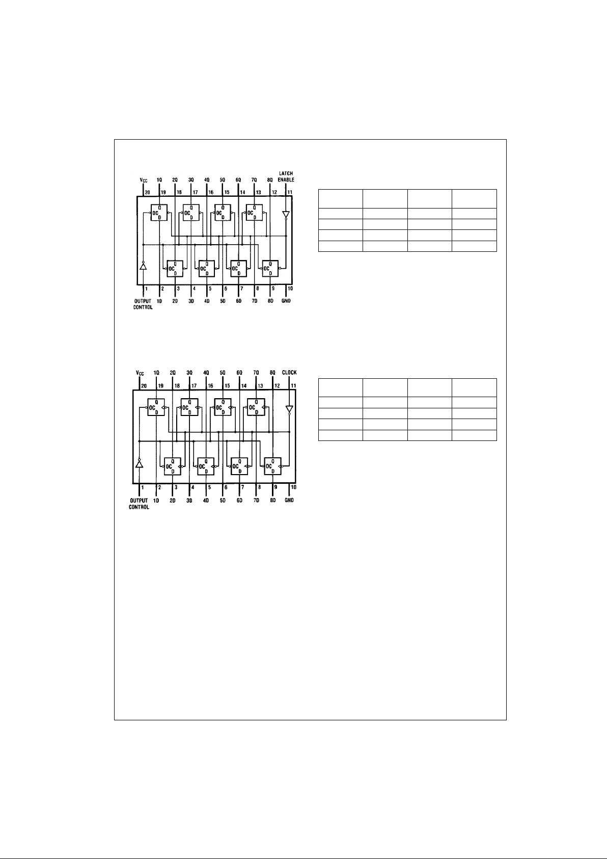
Connection Diagrams
Top View
MM74HCT573
Top View
MM74HCT574
Tr uth Tables
MM74HCT573
H = HIGH Level
L = LOW Level
Q0 = Level of output before steady-state input conditions were est ablished.
Z = High Impedance State
MM74HCT574
H = HIGH Level
L = LOW Level
Q0 = Level of output before steady-state input conditions were est ablished.
X = Don’t Care
Z = High Impedance State
↑ = Transition from LOW-to-HIGH
Output
Control
LE Data Output
LHHH
LHLL
LLXQ
0
HXXZ
Output
Control
LE Data Output
L ↑ HH
L ↑ LL
LLXQ
0
HXXZ

3 www.fairchildsemi.com
MM74HCT573 • MM74HCT574
Absolute Maximum Ratings(Note 1)
(Note 2)
Recommended Operating
Conditions
Note 1: Absolute Maximum Ra tings are those valu es beyond w hich dam-
age to the device may occur.
Note 2: Unless otherwise specified all voltages are referenced to ground.
Note 3: Power Dissipation te mperature d erating — pl astic “N” pa ckage: −
12 mW/°C from 65°C to 85°C.
DC Electrical Characteristics
VCC = 5V ± 10% (unless otherwise specified)
Note 4: Measured pe r pin. All others tied to VCC or ground.
Supply Voltage (VCC) −0.5 to +7.0V
DC Input Voltage (V
IN
) −1.5 to VCC+ 1.5V
DC Output Voltage (V
OUT
) −0.5 to VCC+ 0.5V
Clamp Diode Current (I
IK
, IOK) ± 20 mA
DC Output Current, per pin (I
OUT
) ± 35 mA
DC V
CC
or GND Current, per pin (ICC) ± 70 mA
Storage Temperature Range (T
STG
) −65°C to +150°C
Power Dissipation (P
D
)
(Note 3) 600 mW
S. O. Package only 500 mW
Lead Temperature (T
L
)
(Solderi ng 10 seconds) 260°C
Min Max Units
Supply Voltage (V
CC
)4.55.5V
DC Input or Output Voltage
(V
IN
, V
OUT
)0V
CC
V
Operating Temperature Range (T
A
) −40 +85 °C
Input Rise or Fall Times
t
r
, t
f
500 ns
Symbol Parameter Conditions
TA = 25°CTA = −40 to 85°CTA = −55 to 125°C
Units
Typ Guaranteed Limits
V
IH
Minimum HIGH Level
2.0 2.0 2.0 V
Input Voltage
V
IL
Maximum LOW Level
0.8 0.8 0.8 V
Input Voltage
V
OH
Minimum HIGH Level VIN = VIH or V
IL
V
Output Voltage |I
OUT
| = 20 µAV
CCVCC
− 0.1 VCC − 0.1 VCC − 0.1
|I
OUT
| = 6.0 mA, VCC = 4.5V 4.2 3.98 3.84 3.7
|I
OUT
| = 7.2 mA, VCC = 5.5V 5.7 4.98 4.84 4.7
V
OL
Maximum LOW Level VIN = VIH or V
IL
V
Voltage |I
OUT
| = 20 µA 0 0.1 0.1 0.1
|I
OUT
| = 6.0 mA, VCC = 4.5V 0.2 0.26 0.33 0.4
|I
OUT
| = 7.2 mA, VCC = 5.5V 0.2 0.26 0.33 0.4
I
IN
Maximum Input VIN = VCC or GND,
±0.1 ±1.0 ±1.0 µA
Current VIH or V
IL
I
OZ
Maximum 3-STATE V
OUT
= VCC or GND
±0.5 ±5.0 ±10 µAOutput Leakage Enable = VIH or V
IL
Current
I
CC
Maximum Quiescent VIN = VCC or GND
8.0 80 160 µA
Supply Current I
OUT
= 0 µA
VIN = 2.4V or 0.5V (Note 4) 1.5 1.8 2.0 mA
