Fairchild Semiconductor MM74HCT00SJ, MM74HCT00MX, MM74HCT00MTC, MM74HCT00CW, MM74HCT00SJX Datasheet
...
February 1984
Revised February 1999
MM74HCT00 Quad 2 Input NAND Gate
© 1999 Fairchild Semiconductor Corporation DS005356.prf www.fairchildsemi.com
MM74HCT00
Quad 2 Input NAND Gate
General Description
The MM74HCT00 is a NAND gates fabricated using
advanced silicon-gate CMOS technology which provides
the inherent benefit s of CMOS—low qui escent power and
wide power supply range. This device is input and outp ut
characteristic and pin-out compatible with standar d 74LS
logic families. All inputs are protected from static discharge
damage by internal diodes to V
CC
and ground.
MM74HCT devices are intended to i nterface between TTL
and NMOS components and standard CMOS devices.
These parts are also plug-in replacements for LS-TTL
devices and can be used to redu ce power consumption in
existing designs.
Features
■ TTL, LS pin-out and threshold compatible
■ Fast switching: t
PLH
, t
PHL
=14 ns (typ)
■ Low power: 10 µW at DC
■ High fan out, 10 LS-TTL loads
Ordering Code:
Devices also available in Tape and Reel. Specify by appending the suffix letter “X” to t he ordering code.
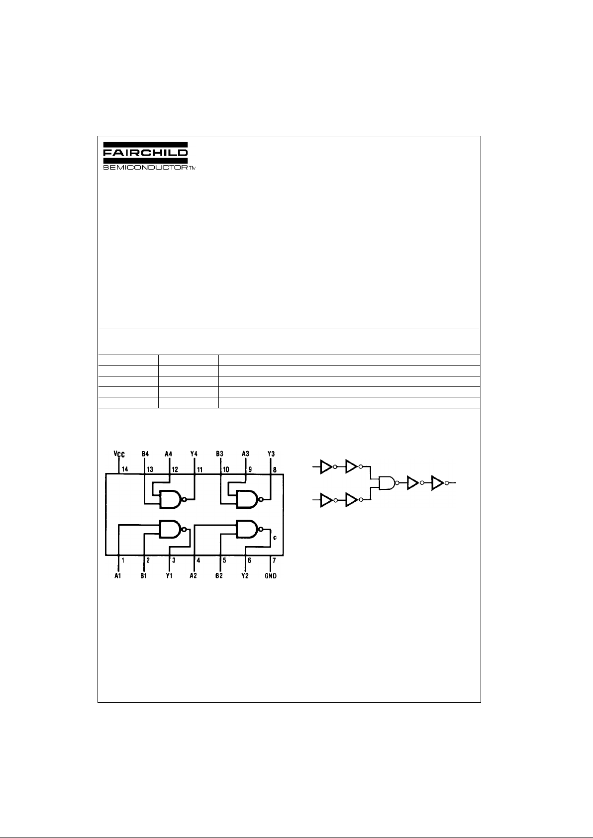
Connection Diagram
Pin Assignments for DIP, SOIC, SOP and TSSOP
Top View
Logic Diagram
(1 of 4 gates)
Order Number Package Number Package Description
MM74HCT00M M14A 14-Lead Small Outline Integrate Circuit (SOIC), JEDEC MS-120, 0.150” Narrow
MM74HCT00SJ M14D 14-Lead Small Outline Package (SOP), EIAJ TYPE II, 5.3mm Wide
MM74HCT00MTC MTC14 14-Lead Thin Shrink Small Outline Package (TSSOP), JEDEC MO-153, 4.4mm Wide
MM74HCT00N N14A 14-Lead Plastic Dual-In-Line Package (PDIP), JEDEC MS-001, 0.300” Wide

www.fairchildsemi.com 2
MM74HCT00
Absolute Maximum Ratings(Note 1)
(Note 2)
Recommended Operating
Conditions
Note 1: Absolute Maximum Ratin gs ar e tho se va lues beyond wh ich d am-
age to the device may occur.
Note 2: Unless otherwise specified all voltages are referenced to ground.
Note 3: Power Dissipation temperatur e derat ing — pl astic “N” p ackage : −
12 mW/°C from 65 °C to 85°C.
DC Electrical Characteristics
VCC = 5V ± 10% (unless otherwise specified)
Note 4: This is measured per input with all other inputs held at VCC or ground.
Supply Voltage (VCC) −0.5 to +7.0V
DC Input Voltage (V
IN
) −1.5 to VCC+1.5V
DC Output Voltage (V
OUT
) −0.5 to VCC+0.5V
Clamp Diode Current (I
IK
, IOK) ±20 mA
DC Output Current, per pin (I
OUT
) ±25 mA
DC V
CC
or GND Current, per pin (ICC) ±50 mA
Storage Temperature Range (T
STG
) −65°C to +150°C
Power Dissipation (P
D
)
(Note 3) 600 mW
S.O. Package only 500 mW
Lead Temperature (T
L
)
(Soldering 10 seconds) 260°C
Min Max Units
Supply Voltage (V
CC
)4.55.5V
DC Input or Output Voltage 0 V
CC
V
(V
IN
, V
OUT
)
Operating Temperature Range (T
A
) −40 +85 °C
Input Rise or Fall Times
(t
r
, tf)500ns
Symbol Parameter Conditions
TA = 25°CTA = −40 to 85°CTA = -55 to 125°C
Units
Typ Guaranteed Limits
V
IH
Minimum HIGH Level 2.0 2.0 2.0 V
Input Voltage
V
IL
Maximum LOW Level 0.8 0.8 0.8 V
Input Voltage
V
OH
Minimum HIGH Level V
IN
= VIH or V
IL
Output Voltage |I
OUT
| = 20 µAV
CCVCC
−0.1 VCC−0.1 VCC−0.1 V
|I
OUT
| = 4.0 mA, V
CC
= 4.5V 4.2 3.98 3.84 3.7 V
|I
OUT
| = 4.8 mA, V
CC
= 5.5V 5.2 4.98 4.84 4.7 V
V
OL
Maximum LOW Level V
IN
= V
IH
Voltage |I
OUT
| = 20 µA00.10.10.1V
|I
OUT
| = 4.0 mA, VCC = 4.5V 0.2 0.26 0.33 0.4 V
|I
OUT
| = 4.8 mA, V
CC
= 5.5V 0.2 0.26 0.33 0.4 V
I
IN
Maximum Input V
IN
= VCC or GND, ±0.05 ±0.5 ±1.0 µA
Current VIH or V
IL
I
CC
Maximum Quiescent V
IN
= VCC or GND, 1.0 10 40 µA
Supply Current I
OUT
= 0 µA
V
IN
= 2.4V or 0.5V (Note 4) 0.18 0.3 0.4 0.5 mA
 Loading...