

Fairchild Semiconductor ML6554 Datasheet
www.fairchildsemi.com
ML6554
3A Bus Termination Regulator
Features
• Can source and sink up to 3A, no heat sink required
• Integrated Power MOSFETs
• Generates termination voltages for DDR SDRAM,
SSTL-2 SDRAM, SGRAM, or equivalent memories
• Generates termination voltages for active termination
schemes for DDR SDRAM, GTL+, Rambus, VME,
LV-TTL, HSTL, PECL and other high speed logic
•V
• Separate voltages for V
• Buffered V
•V
input available for external voltage divider
REF
output
REF
of ±3% or less at 3A
OUT
CCQ
and PV
DD
• Minimum external components
• Shutdown for standby or suspend mode operation
• 0° to +70°C and -40° to +85°C temperature ranges
available
• Thermal Shutdown ≈ 130ºC
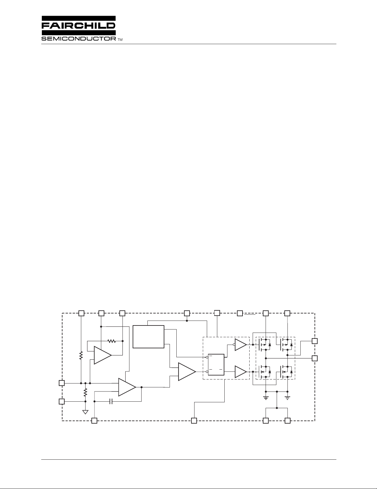
Block Diagram
Description
The ML6554 switching regulator is designed to convert voltage supplies ranging from 2.3V to 4V into a desired output
voltage or termination voltage for various applications. The
ML6554 can be implemented to produce regulated output
voltages in two different modes. In the default mode, when
the V
the voltage applied to V
to produce various user-defined voltages by forcing a voltage
on the VREF
the input VREF
ble of sourcing or sinking up to 3A of current while regulating an output V
The ML6554, used in conjunction with series termination
resisitors, provides an excellent voltage source for active
termination schemes of high speed transmission lines as
those seen in high speed memory buses and distributed
backplane designs. The voltage output of the regulator can
be used as a termination voltage for other bus interface
standards such as DDR SDRAM, SSTL, CMOS, Rambus
GTL+, VME, LV-CMOS, LV-TTL, HSTL and PECL.
pin is open, the ML6554 output voltage is 50% of
REF
pin. In this case, the output voltage follows
IN
voltage. The switching regulator is capa-
IN
voltage to within 3% or less.
TT
. The ML6554 can also be used
CCQ
™
,
11
13
200kΩ
VREF
200kΩ
AGND
D
GND
9
S
R
12
V
DD
Q
Q
SHDN
2
4 58
PV
P
GND1
DD1
7
PV
DD2
V
L1
(V
)
OUT
3
6
V
L2
(V
)
OUT
P
GND2
15
IN
V
CCQ
10
16
–
+
V
V
FB
AV
REF
14
CC
BUFFER
+
–
VREF
OUT
OSCILLATOR/
RAMP
GENERATOR
ERROR AMP
1
V
DD
–
+
RAMP
COMPARATOR
REV. 1.1.3 3/8/02
2
ML6554 PRODUCT SPECIFICATION
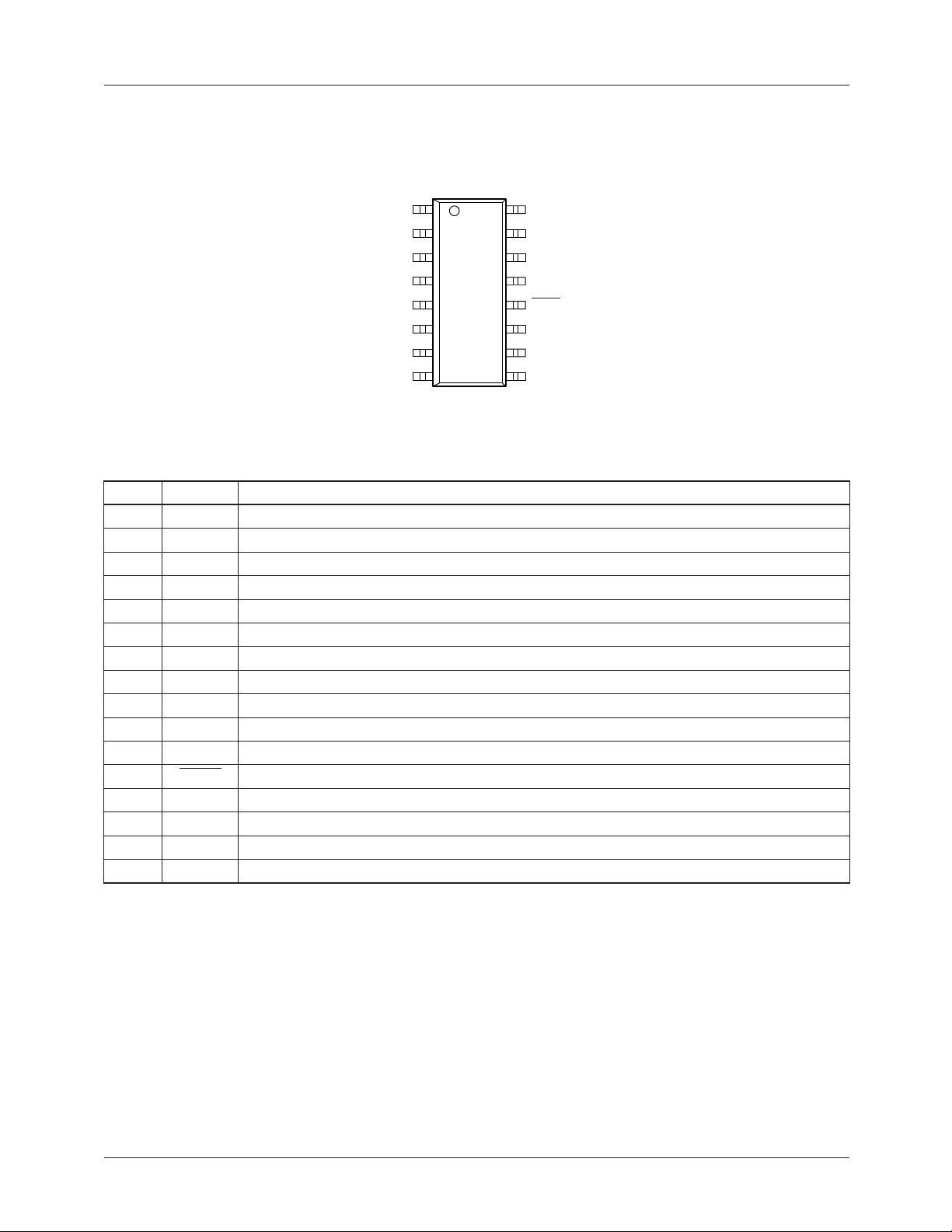
Pin Configuration
ML6554
16-Pin PSOP (U16)
Pin Description
Pin Name Function
1V
2PV
3V
4P
5P
6V
7PV
8D
9V
10 V
11 VREF
12 SHDN Shutdown active low. CMOS input level
13 AGND Ground for internal reference voltage divider
14 VREF
15 V
16 AV
DD
DD1
L1
GND1
GND2
L2
DD2
GND
DD
FB
OUT
CCQ
CC
PV
P
GND1
P
GND2
PV
D
V
DD
DD1
V
V
DD2
GND
L1
L2
1
2
3
4
5
6
7
8
TOP VIEW
Digital supply voltage
Voltage supply for internal power transistors
Output voltage/ inductor connection
Ground for output power transistors
Ground for output power transistors
Output voltage/inductor connection
Voltage supply for internal power transistors
Digital ground
Digital supply voltage
Input for external compensation feedback
Input for external reference voltage
IN
Reference voltage output
Voltage reference for internal voltage divider
Analog voltage supply
AV
16
15
14
13
12
11
10
9
CC
V
CCQ
VREF
AGND
SHDN
VREF
V
FB
V
DD
OUT
IN
REV. 1.1.3 3/8/02
∆
PRODUCT SPECIFICATION ML6554
Absolute Maximum Ratings
Absolute maximum ratings are those values beyond which the device could be permanently damaged. Absolute maximum
ratings are stress ratings only and functional device operation is not implied.
Parameter Min. Max. Units
PV
DD
Voltage on Any Other Pin GND – 0.3 V
Average Switch Current (I
) 3.0 A
AVG
4.5 V
+ 0.3 V
IN
Junction Temperature 150 °C
Storage Temperature Range -65 150 °C
Lead Temperature (Soldering, 10 sec) 150 °C
Thermal Resistance ( θ
)(Note 2) 2 °C/W
JC
Output Current, Source or Sink 3.0 A
Operating Conditions
Parameter Min. Max. Units
Temperature Range, CU suffix 0 70 °C
Temperature Range, IU suffix -40 +85 °C
PV
Operating Range 2.0 4.0 V
DD
V
Operating Range 1.4 4.0 V
CCQ
Electrical Characteristics
Unless otherwise specified, AV
Symbol Parameter Conditions Min. Typ. Max. Units
Switching Regulator
V
TT
Output Voltage, SSTL_2
(See Figure 1)
VREF
Z
IN
Internal Resistor Divider I
OUT
V
Reference Pin Input
REF
Impedance
Switching Frequency 650 kHz
V
OFFSET
Offset Voltage V
Supply
I
Q
Quiescent Current I
Buffer
I
REF
Notes
1. Limits are guaranteed by 100% testing, sampling, or correlation with worst-case test conditions.
2. Infinite heat sink
Output Load Current 3 mA
= V
CC
– VREF
TT
DD
= PV
OUT
= 3.3V ±10%, TA = Operating Temperature Range (Note 1)
DD
I
= 0,
OUT
V
= open
REF
I
= ±3A,
OUT
V
= open
REF
= 0 V
OUT
AV
= 2.5V No Load V
CC
= 0, no load
OUT
V
= 2.5V
CCQ
V
= 2.3V 1.12 1.15 1.18 V
CCQ
V
= 2.5V 1.22 1.25 1.28 V
CCQ
V
= 2.7V 1.32 1.35 1.38 V
CCQ
V
= 2.3V 1.09 1.15 1.21 V
CCQ
V
= 2.5V 1.19 1.25 1.31 V
CCQ
V
= 2.7V 1.28 1.35 1.42 V
CCQ
= 2.3V 1.139 1.15 1.162 V
CCQ
V
= 2.5V 1.238 1.25 1.263 V
CCQ
V
= 2.7V 1.337 1.35 1.364 V
CCQ
V
= 0 100 k Ω
CCQ
= 2.5 –20 20 mV
CCQ
I
VCCQ
I
AVCC
I
SD 0.2 0.5 mA
AVCC
I
VDD
I
SD 0.2 1.0 mA
VDD
I
PVDD
610µA
0.5 1.0 mA
0.25 1.0 mA
100 250 µA
REV. 1.1.3 3/8/02
3
4
ML6554 PRODUCT SPECIFICATION
Functional Description
This switching regulator is capable of sinking and sourcing
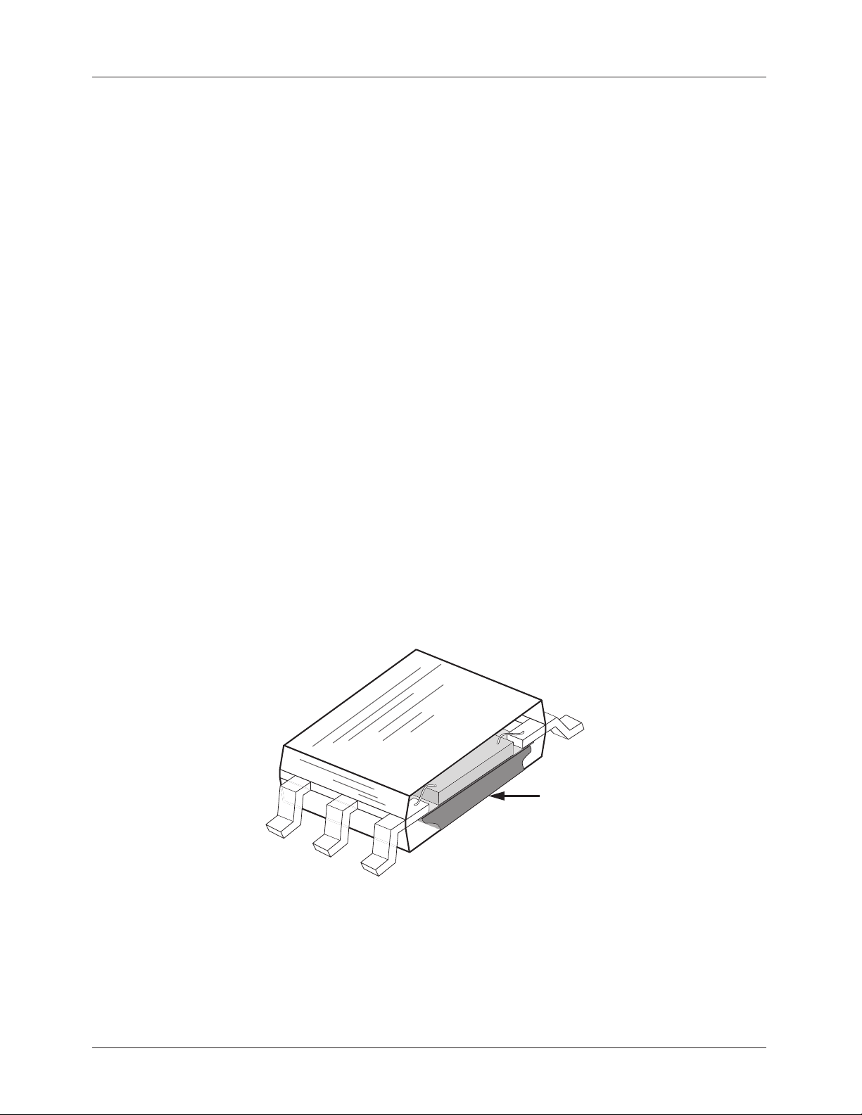
3A of current without an external heatsink. The ML6554
uses a power surface mount package (PSOP) that includes
an integrated heat slug. The heat can be piped through the
bottom of the device and onto the PCB (Figure 1).
The ML6554 integrates two power MOSFETs that can be
used to source and sink 3A of current while maintaining a
tight voltage regulation. Using the external feedback, the
output can be regulated well within 3% or less, depending on
the external components chosen. Separate voltage supply
inputs have been added to accommodate applications with
various power supplies for the databus and power buses, see
Figure 2.
Outputs
The output voltage pins (V
address, or clock lines via an external inductor. See the
Applications section for recommendations. Output voltage
is determined by the V
Inputs
The input voltage pins (V
output voltages (V
the VREF
V
input. V
CCQ
databus.
IN
L1
pin is floating, the output voltage is 50% of the
can be the reference voltage for the
CCQ
, V
) are tied to the databus,
L1
L2
or VREF
CCQ
or VREF
CCQ
or V
) . In the default mode, where
L2
inputs.
IN
) determine the
IN
Output voltage can also be selected by forcing a voltage at
the VREF
voltage at the VREF
pin. In this case, the output voltage follows the
IN
input. Simple voltage dividers can be
IN
used this case to produce a wide variety of output voltages
between 0.7V and V
DD
–0.7V.
VREF Input and Output
The VREF
outputs (Inputs section, above). The VREF
output pin that is driven by a small output buffer to provide
the V
buffer is capable of driving several output loads. The output
buffer can handle 3mA.
input can be used to force a voltage at the
IN
signal to other devices in the system. The output
REF
OUT
pin is an
Other Supply Voltages
Several inputs are provide for the supply voltages: PV
PV
, AV
DD1
, and VDD.
CC
and PV
provide the power supply to the
DD2
DD2
The PV
power MOSFETs. VDD provides the voltage supply to the
digital sections, while AVCC supplies the voltage for the
analog sections. Again, see the Applications section for
recommendations.
DD1
,
Feedback Input
The VFB pin is an input that can be used for closed loop
compensation. This input is derived from the voltage output.
See application section for recommendation.
Figure 1. Cutaway view of PSOP Package
HEAT SLUG
REV. 1.1.3 3/8/02
PRODUCT SPECIFICATION ML6554
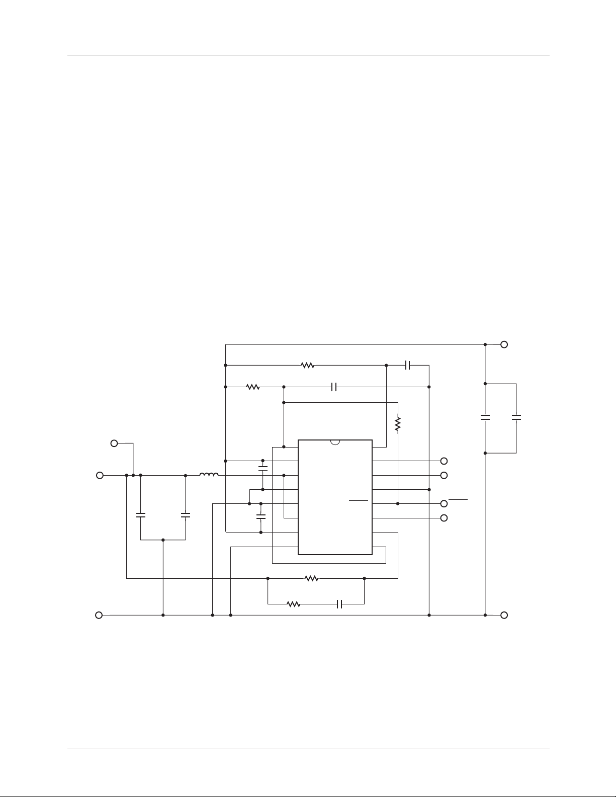
Applications
Using the ML6554 for SSTL Bus Termination
The circuit schematic in Figure 2 shows a recommended
approach for constructing a bus terminating solution for an
SSTL-2 bus. This circuit can be used in PC memory and
Graphics memory applications as shown in Figures 4 and 5.
Note that the ML6554 can provide the voltage reference
(V
) and terminating voltages (VTT). Using the layout
REF
as shown in Figures 6, 7, and 8, and measuring the VTT
performance using the test setup as described in Figure 9,
the ML6554 delivered a V
(see Figure 10). Table 1 provides a recommended parts list
for the circuit in Figure 2.
± 20mV for 1A to 3A loads
TT
Power Handling Capability of the PSOP
Package
Using the board layout shown in Figures 6, 7, and 8; soldering the ML6554 to the board at zero LFPM the temperature
around the package measured 55ºC for 3A loads. Note that a
1 ounce copper plane was used in the board construction.
Airflow is not likely to be needed in the operation of this
device (assuming a board layout similar to that described
above). The power handling performance of the PSOP
package is shown by a study of the package manufacturer for
various airflow vs. θ
conditions in Figure 11.
JA
Bus Termination Solutions for Others Buses
Table 3 provides a summary of various bus termination V
& VTT requirements. The ML6554 can be used for those
applications.
R2 100Ω
C8 0.1µF
REF
2.5V TO 4V
TPI
V
TT
TO SDRAMS
C1
820µF
F2V
OS-CON
L1 3.3µH
C2
0.1µF
R1 100Ω
C3 0.1µF
C4 0.1µF
1
V
2
PV
3
V
4
P
5
P
6
V
7
PV
8
D
R4 100kΩ
R5 1kΩ
Figure 2.
C9 0.1µF
ML6554
DD
DD1
L1
GND1
GND2
L2
DD2
GND
U1
VREF
C7 1nF
AV
V
CCQ
OUT
AGND
SHDN
VREF
V
OUT
IN
C5
330µF 330µF
R3
100kΩ
16
CC
15
14
13
12
11
IN
10
V
FB
9
DD
V
CCQ
VREF
SHDN
VREF
C6
GNDGND
REV. 1.1.3 3/8/02 5
 Loading...