

Fairchild Semiconductor KSE13007, KSE13006 Datasheet
KSE13006/13007
High Voltage Switch Mode Application
• High Speed Switching
• Suitable for Switching Regulator and Motor Control
KSE13006/13007
1
TO-220
1.Base 2.Collector 3.Emitter
NPN Silicon Transistor
Absolute Maximum Ratings
Symbol Parameter Value Units
V
CBO
Collector-Base Voltage : KSE13006
V
CEO
Collector-Emitter Voltage : KSE13006
V
I
C
ICP
IB
P
T
T
EBO
C
J
STG
Emitter- Base Voltage 9 V
Collector Current (DC) 8 A
Collector Current (Pulse) 16 A
Base Current 4 A
Collector Dissipation (TC=25°C) 80 W
Junction Temperature 150 °C
Storage T emperature - 65 ~ 150 °C
Electrical Characteristics
Symbol Parameter Test Condition Min. Typ. Max. Units
BV
CEO
I
EBO
h
FE
(sat) *Collector-Emitter Saturation Voltage IC = 2A, IB = 0.4A
V
CE
(sat) *Base-Emitter Saturation Voltage IC = 2A, IB = 0.4A
V
BE
C
ob
f
T
t
ON
t
STG
t
F
* Pulse test: PW≤300µs, Duty cycle≤2%
Collector- Emitter Breakdown Voltage
Emitter Cut-off Current V
*DC Current Gain
Output Capacitance V
Current Gain Bandwidth Product V
Turn On Time V
Storage Time 3 µs
Fall Time 0.7 µs
TC=25°C unless otherwise noted
: KSE13007
: KSE13007
TC=25°C unless otherwise noted
: KSE13006
= 10mA, IB = 0 300
I
C
: KSE13007
= 9V, IC = 0 1 mA
EB
V
= 5V, IC = 2A
CE
= 5V, IC = 5A
V
CE
= 5A, IB = 1A
I
C
I
= 8A, IB = 2A
C
= 5A, IB = 1A
I
C
= 10V, f = 0.1MHz 110 pF
CB
= 10V, IC = 0.5A 4 MHz
CE
= 125V, IC = 5A
CC
I
= -IB2 = 1A
B1
= 50Ω
R
L
400
8
5
600
700
300
400
60
30
1
2
3
1.2
1.6
1.6 µs
V
V
V
V
V
V
V
V
V
V
V
©2000 Fairchild Semiconductor International Rev. A1, December 2000
Typical Characteristics
KSE13006/13007
100
10
, DC CURRENT GAIN
FE
h
1
0.1 1 10
IC[A], COLLECTOR CURRENT
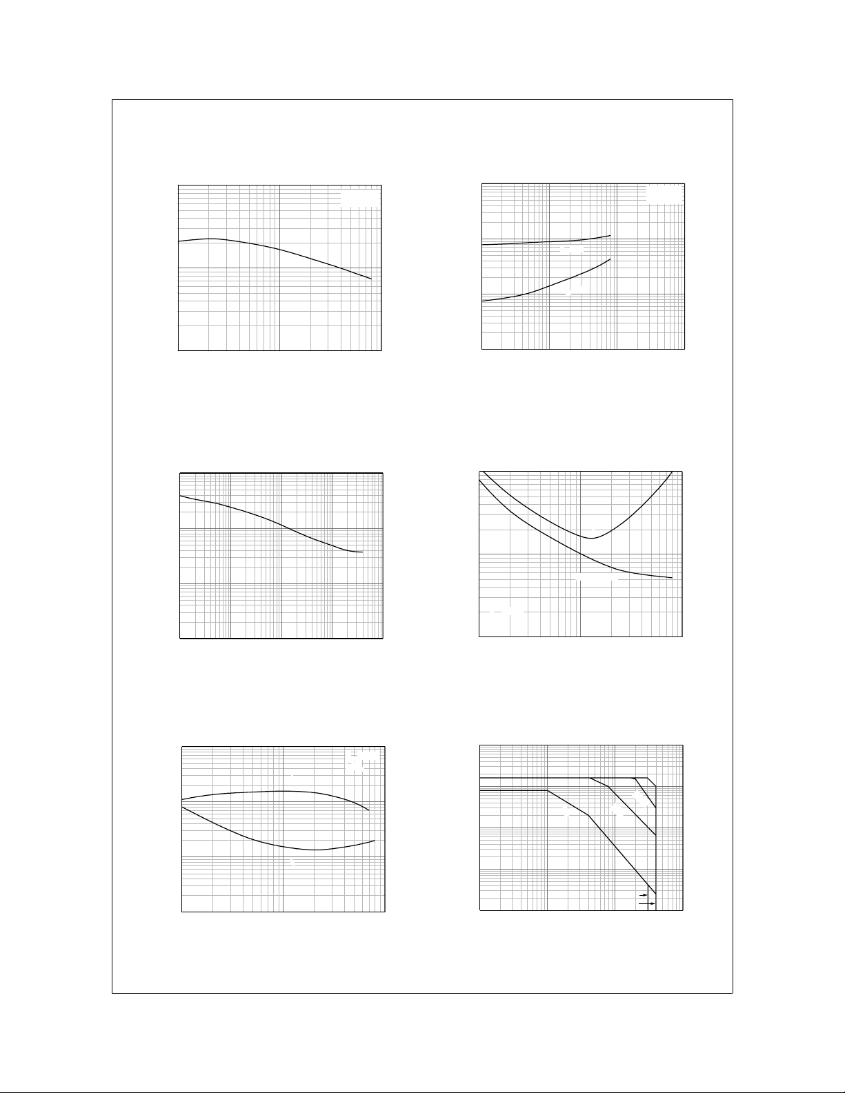
Figure 1. DC current Gain Figure 2. Base-Emitter Saturation Voltage
1000
100
10
[pF], OUTPUT CAPACITANCE
ob
C
1
0.1 1 10 100 1000
VCB[V], COLLECTOR-BASE VOLTAGE
VCE = 5V
VBE(sat)
VCE(sat)
IC = 3 I
B
10
1
0.1
(sat)[V], SATURATION VOLTAGE
CE
(sat), V
BE
V
0.01
0.1 1 10 100
IC[A], COLLECTOR CURRENT
Collector-Emitter Saturation Voltage
1000
100
s], TURN ON TIME
µ
[
D
, t
R
t
VCC=125V
IC=5I
B
10
0.1 1 10
IC[A], COLLECTOR CURRENT
t
R
tD, VBE(off)=5V
Figure 3. Collector Output Capacitance Figure 4. Turn On Time
10000
1000
s], TURN OFF TIME
µ
[
F
100
, t
STG
t
10
0.1 1 10
Figure 5. Turn Off Time Figure 6. Safe Operating Area
©2000 Fairchild Semiconductor International
t
STG
t
F
IC[A], COLLECTOR CURRENT
VCC=125V
IC=5I
B
100
10
1
0.1
[A], COLLECTOR CURRENT
C
I
0.01
1 10 100 1000
100
µ
s
DC
1ms
KSE13006
KSE13007
VCE[V], COLLECTOR-EMITTER VOLTAGE
Rev. A1, December 2000
 Loading...