Fairchild Semiconductor KA7541 Datasheet

KA7541
Simple Ballast Controller
www.fairchildsemi.com
Features
• Internal soft start
• Flexible soft start frequency
• No lamp protection
• Trimmed 1.5% internal bandgap reference
• Under voltage lock out with 1.8V of hysteresis
• Totem pole output with high state clamp
• Low start up and operating current
Descriptions
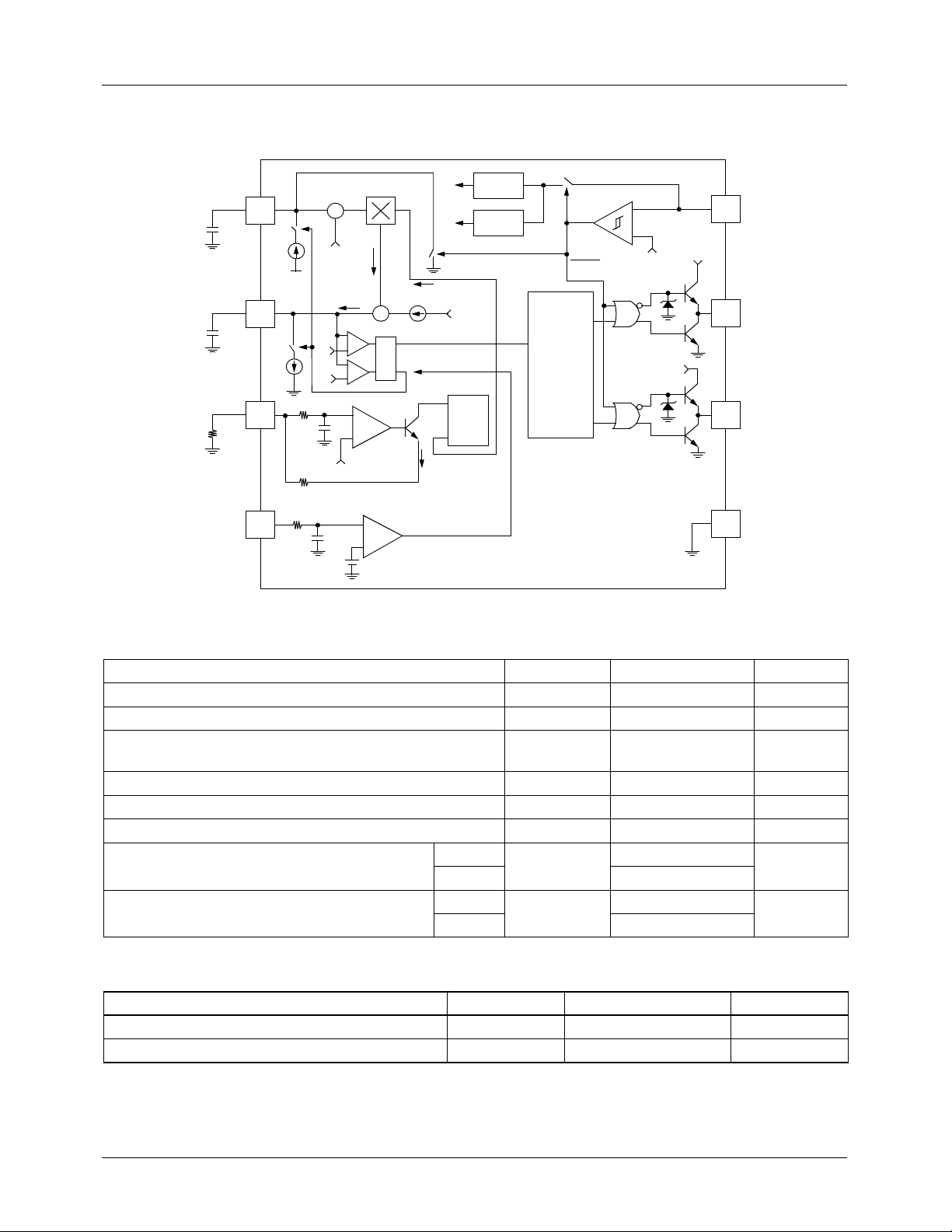
The KA7541 provides simple and high performance
electronic ballast control functions. KA7541 is optimized for
electronic ballast requiring a minimum b oard area, reduced
component count and low power dissipation. Internal soft
start circuitry eliminates the need for an external soft sta rt
PTC resistor. The initial soft start switching frequency and
soft start time can be adjusted depending on the types of
lamps. Protection circuitry has also been adde d to prevent
burning out of switches in no lamp condition. output gate
drive circuit clamps power MOSFET gate voltage
irrespective of supply voltage
8-DIP
1
8-SOP
1
©2001 Fairchild Semiconductor Corporation
Rev. 1.0.3

KA7541
Internal Block Diagram
0.22µF
180pF
22k
1.8V
UVLO
+
−
9.5V
8
V
CC
V
CC
OUT 1
7
V
CC
OUT 2
6
GND
5
2V Ref
V
40k
30k
5pF
Z
3pF
2k
−
+
Vref
I
H
I
+
S
R
latch
+
Q
C
Oscilator
I
S
Shut down signal
Ict
+
-
3V
-
+
1V
Ω
−
+
Vref
Ω
Ω
−
+
2V
Ik = IS / 6
Oscilator
Current
mirror
Internal
bias
UVLO
F.D
Frequency
divider
I
= Ik × (Vref − VSS) / Vref
H
= Vref / RS
I
S
Ldet
1
2.5µA
2
8Ict
3
4
C
S
Ct
R
S
Ω
Absolute Maximum Ratings
Parameter Symbol Value Unit
Supply voltage V
Peak drive output current I
Drive output clamping diodes
V
O>VCC
, or VO<−0.3
OH
Iclamp ±10 mA
Soft start, and no lamp detection input voltage V
CC
, I
IN
OL
30 V
±300 mA
−0.3 to 6 V
Operating temperature range Topr -25 to 125 °C
Storage temperature range Tstg −65 to 150 °C
Power dissipation
Thermal resistance (Junction-to-air)
8-DIP
8-SOP 0.5
8-DIP
8-SOP 165
Pd
θja
0.8
100
Absolute Maximum Ratings (-25°°°°C≤≤≤≤Ta≤≤≤≤125°°°°C)
Parameter Symbol Value Unit
Temperature stability for reference voltage (Vref) ∆Vref(Typ) 15 mV
Temperature stability for operating frequency (fos) ∆fos(Typ) 5 kHz
W
°C/W
2

Pin Assignments
KA7541
V
1
S
CC
8C
Ct
R
Ldet
2
S
3
4
7
6
5
(Top View)
Pin Definitions
Pin Number Pin Name Pin Function Descrition
1C
2C
3R
S
T
S
4 Ldet
5 GND The ground potential of all the pins.
6OUT 2
7OUT 1
8V
CC
Soft start capacitor connection pin. The pin voltage determines the phase of soft
start, normal mode.
Timing capacitor connection pin. The timing capacitor is charged and discharged
to generate the sawtooth waveform that determines the oscillation frequency in
the internal oscillator block.
Soft start resistor connection pin. The soft start resistor value determines the initial
preheating switching frequency during soft start mode.
Input to the protection circuit. If the pin voltage is lower than 2V, the output of the
gate driver is inhibited.
The output of a high-current power driver capable of driving the gate of a power
MOSFET
The output of a high-current power driver capable of driving the gate of a power
MOSFET.
The logic and control power supply connection.
OUT1
OUT2
GND
3

KA7541
Electrical Characteristics
o
Unless otherwise specified, for typical values Vcc=14V, Ta=25
temperature range with
-25
o
≤ Ta ≤ 125
C
o
C
and 11V ≤ V
CC
Parameter Symbol Conditions Min. Typ. Max. Unit
UNDER VOLTAGE LOCK OUT SECTION
Start threshold voltage V
UVLO hysteresis HY
TH(st)
(st)
SUPPLY CURRENT SECTION
Start up supply current I
Operating supply current I
Dynamic operating supply current I
ST
CC
DCC
REFERENCE SECTION
Reference voltage V
Line regulation ∆V
Temperature stability of Vref ∆V
ref
ref 1
ref 2
OSCILLATOR SECTION
Operating frequency fos V
Operating dead time tod V
Soft start frequency fss V
Soft start dead time tsd V
OUTPUT SECTION
Rising time
Falling time
Maximum output voltage V
Output voltage with UVLO activated V
(note1)
(note1)
tr CI=1nF, Vcc=12V - 120 200 ns
tf CI=1nF, Vcc=12V - 50 100 ns
omax(o)VCC
omin(o)
NO LAMP PROTECTION SECTION
No lamp detect voltage Vnd - 1.9 2 2.1 V
Note:
1. These parameters, although guaranteed, are not 100% tested in production.
C, For Min/Max values Ta is the operating ambient
≤ 30V
VCC increasing 8.5 9.5 10.5 V
- 1.3 1.8 2.3 V
VCC<VTH(st) - 0.15 0.25 mA
Output not switching - 6 10 mA
50kHz, CI=1nF - 7 14 mA
Iref=0mA, Vcc=14V 1.95 2 2.05 V
14V≤V
≤25V - 0.1 10 mV
CC
-25≤Ta≤125°C, Vcc=14V - 15 - mV
=3V, CT=470pF 44 50 56 KHz
SS
=3V, Vcc=14V 2.4 2.9 3.4 µs
SS
=0V, CT=470pF 56 65 74 KHz
SS
=0V, Vcc=14V 1.8 2.3 2.8 µs
SS
=20V 12 15 18 V
VCC=5V, IO=100µA--1V
4

KA7541
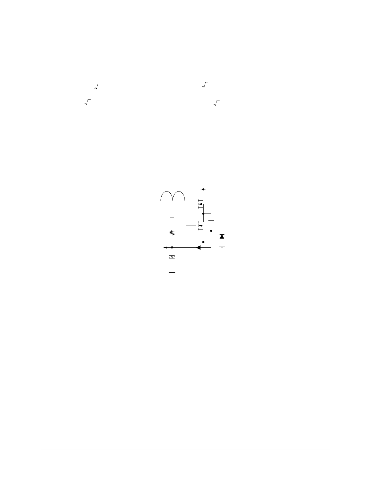
Start-up Circuit
Start up current is supplied to the IC through the start up resistor (Rst). In order to reduce the power dissipation in Rst, the Rst
is connected to the full wave rectified output voltage.
The following equation can be used to calculate the size of Rst
Vin ac() 2Vthst()max,–×
-------------------------------------------------------------------------- -
Rst
<
85 2 10.5–×
------------------------------------- - 440kΩ==
0.25 10
×
Ist max,
3–
P
Vin ac_max()2Vcc–⋅()
----------------------------------------------------------------------- -
RSt
2 Vi n ac_max()2Vcc–⋅()
R
×≥
St
R
St
R
260K≥
St
The size of start up capacitor (Cst) is normally decided in terms o f the start up time a nd operating current build up time with
auxiliary operating current source.
The turn off snubber capacitor (Cq2) and two diodes (D1, D2) constitute the auxiliary operating current source for the IC. The
charging current through the Cq2 flows into the IC and also charges the start-up capacitor. If the size of Cq2 is increased, the
V
voltage of the Cst is also increased.
CC
Q1
2
0.5W≤=
2
260K R
440K≤≤∴
St
Rectifier
To V
(Pin 8)
Output
Rst
CC
+
−
Cst
Q2
D2
Cq2
D1
Figure 1. Start up circuit
Oscillator
The gate drive output frequency is as half as that of the triangular waveform in timing capacitor (Ct) at pin #2. In normal
operating mode, the timing capacitor charging current is 50µA. The discharging current is seven times of the charging current
(7× 50µA). The charging period of the timing capacitor is the on duty of the gate drive. The discharging period is the off duty
of the gate drive.
The rising slope and falling slope of the triangular waveform are as following.
Rising slope: dv / dt = i / C = 50µA / Ct
Falling slope: dv / dt = i / C = 7 × 50µA / Ct
For example, when the timing capacitor is 180pF,
∆Tch = 6.69µ
∆Tdis = 0.956µ
5
 Loading...