

Fairchild Semiconductor KA378R05 Datasheet
KA378R05
Low Dropout Voltage Regulator
www.fairchildsemi.com
Features
• 3A / 5V Output low dropout voltage regulator
• TO220 Full-Mold package (4PIN)
• Overcurrent protection, Thermal shutdown
• Overvoltage protecti on, Short-Circuit protection
• With output disable function
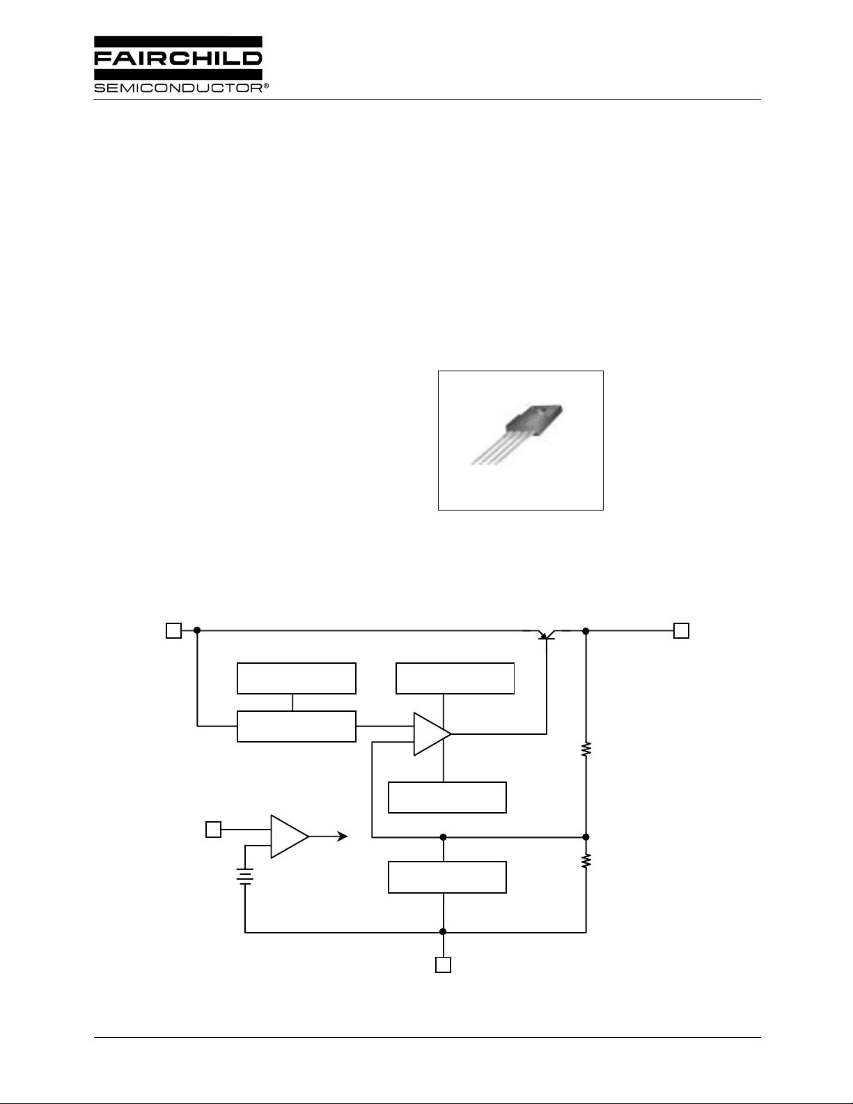
Internal Block Diagram
1
Vin
Description
The KA378R05 is a low-dropout voltage regulator suitable
for various electronic equipments. It provides constant
voltage power source with TO-220 4 lead full mold package.
Dropout voltage of KA378R05 is below 0.5V in full rated
current(3A). This regulator has various function such as
peak current protection, thermal shut down, overvolt age
protection and output disable functio n.
TO-220F-4L
1
1.Vin 2. Vo 3. GND 4. Vdis
Q1
2
Vo
THERMAL SHUTDOWN
BANDGAP REFERENCE
HIGH / LOW OUTPUT
4
Vdis
1.4V
©2001 Fairchild Semiconductor Corporation
+
ON / OFF
OVERVOLTAGE
PROTECTION
+
SOA PROTECTION
SHORT-CIRCUIT
SHORTCIRCUIT
PROTECTION
3
GND
R1
R2
Rev. 1.0.2
KA378R05
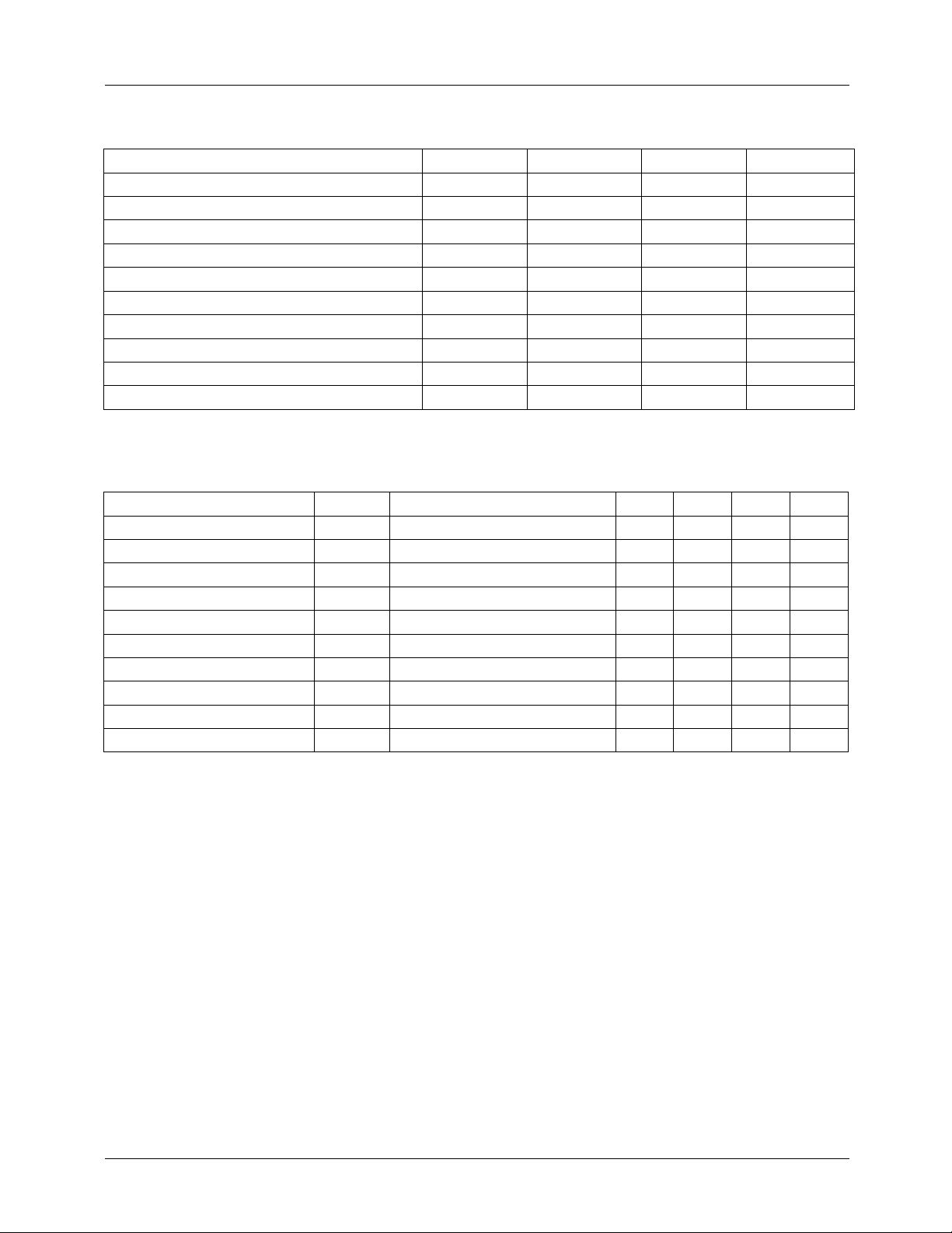
Absolute Maximum Ratings
Parameter Symbol Value Unit Remark
Input Voltage Vin 35 V Disable Voltage Vdis 35 V Output Current Io 3.0 A Power Dissipation 1 Pd1 1.5 W No Heatsink
Power Dissipation 2 Pd2 15 W With Heatsink
Junction Temperature Tj 150 °C-
Operating Temperature Topr -20 ~ 80 °C-
Thermal Resistance, Junction-to-Case(Note2) Rθjc 2.9 °C/W -
Thermal Shutdown Temperature Ttsd 150 °C-
Storage Temperature T
stg
-65 ~ 150 °C-
Electrical Characteristics
(Vin=7V, Io=1.5A, Ta=25°C, unless otherwise specified)
Parameter Symbol Conditions Min. Typ. Max. Unit
Output Voltage Vo - 4.88 5 5.12 V
Load Regulation Rload 5mA < Io < 3A - 0.1 2.0 %
Line Regulation Rline 6V < Vin < 12V - 0.5 2.5 %
Ripple Rejection Ratio RR note1 45 55 - dB
Dropout Voltage Vdrop Io = 3A - - 0.5 V
Disable Voltage High VdisH Output Active 2.0 - - V
Disable Voltage Low VdisL Output Disabled - - 0.8 V
Disable Bias Current High IdisH Vdis = 2.7V - - 20 µA
Disable Bias Current Low IdisL Vdis = 0.4V - - -0.4 mA
Quiescent Current Iq Io = 0A - - 10 mA
Note:
1.These parameters, although guaranteed, are not 100% tested in production.
2. Junction -to-case thermal resistance test enviroments.
-.Pneumatic heat sink fixture.
-.Clamping pressure 60psi through 12mm diameter cylinder.
-.Thermal grease applied between PKG and heat sink fixture.
2
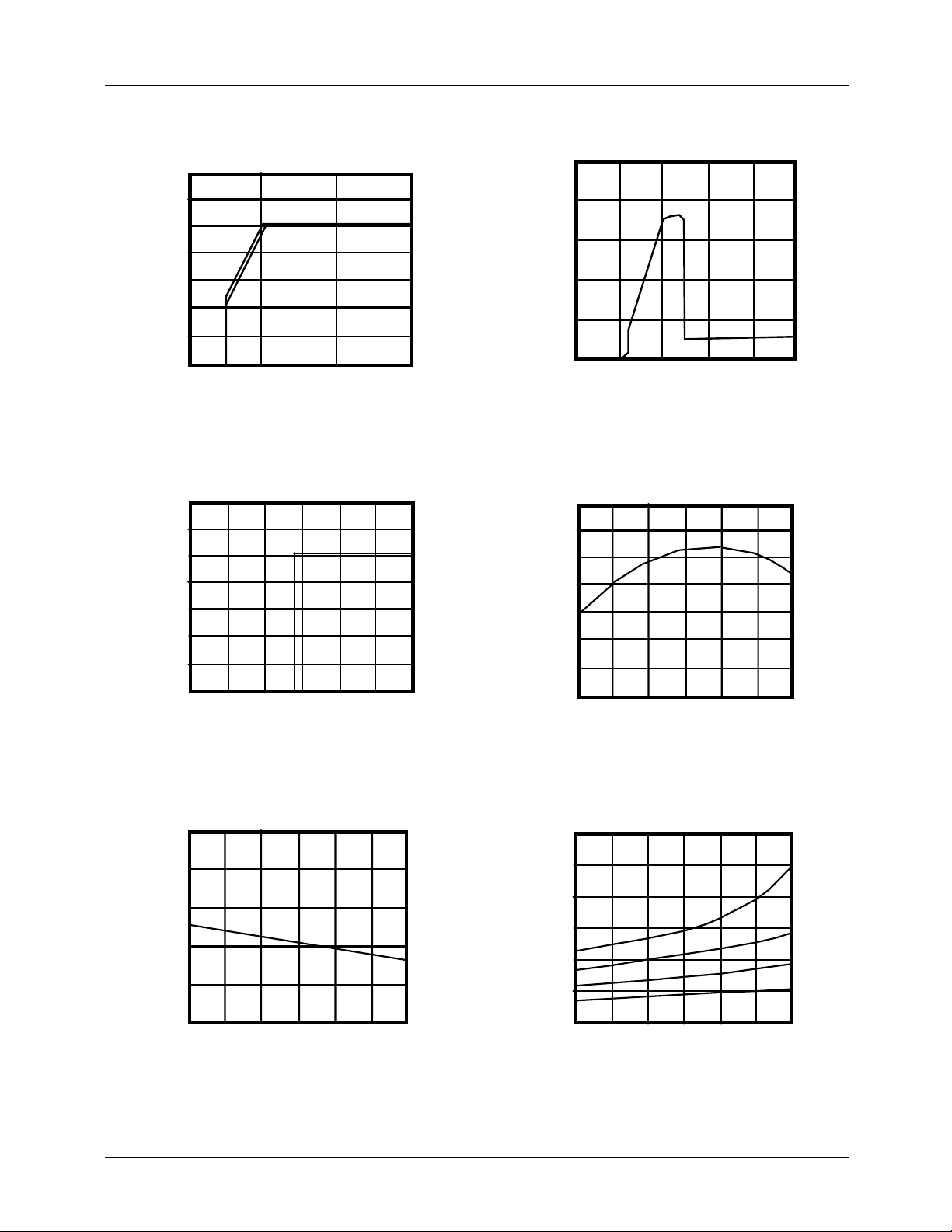
Typical Perfomance Characteristics
7
6
5
4
3
2
Output voltage Vo(V)
1
0
0
8
RL=
Ω
RL=1.7
51015
Input voltage Vin (V)
80
60
40
i
20
Quescent current Iq( m A)
0
0 2 4 6 8 10
RL=
Input voltage Vin (V)
KA378R05
8
Figure 1. Output Voltage vs. Input Voltage
7
6
5
4
3
2
Output voltage Vo(V)
1
0
0
0.5
122.5
1.5
3
Disable voltage Vdis (V)
Figure 3. Output Voltage vs. Disable Voltage
10
8
Figure 2. Quiescent Current vs. Input Voltage
5.06
5.04
5.02
5.00
4.98
4.96
Output voltage Vo(V)
4.94
4.92
-25
02550
TEMPERATURE Tj(oC)
75
100
125
Figure 4. Output Voltage vs. Temper at ure(Tj)
0.6
0.5
6
4
i
2
Quesce nt current Iq(mA)
0
02550
-25
75
100
125
Junction temperature Tj (oC)
Figure 5. Quiescent Current vs. Temperature(Tj)
0.4
0.3
0.2
Dropout voltage Vdrop(V)
0.1
0
02550
-25
Io=3A
2.0A
1.0A
0.5A
75
100
125
Junction temperature Tj(oC)
Figure 6. Dropout Voltage vs. Junction Temperature
3
 Loading...