

Fairchild Semiconductor KA3080C, KA3080BD3 Datasheet

KA3080/KA3080D/KA3080DM
3-Phase BLDC Motor Driver
www.fairchildsemi.com
Features
• 3-Phase, Full-Wave, Linear BLDC Motor Driver With 3
Hall Sensors
• Built-in TSD (Therml Shutdown) Circuit
• Built-in Torque Ripple Control Circuit
• Built-in Output Current Limiter
• Motor Speed Contro l
•High Output Current
• Built-in FG Amplifier With Sinusoidal Waveforms
• Built-in Hall Amplifier
• Built-in CW and CCW Circuit
Description
The KA3080 , KA3080D, KA3080DM are a monolithic
integrated circuit, and it is suitable for 3-phase capstan motor
driver for VCR system.
32-SDIPH-400 28-SSOPH-375
28-SSOPH-375SG2
Target Application
• Video Cassette Recorder (VCR) Capstan Motor
• Other 3-Phase BLDC Motor
©2002 Fairchild Semiconductor Corporation
Ordering Information
Device Package Operating Temp.
KA3080C 32-SDIPH-400 -25°C ~ +75°C
KA3080BD 28-SSOPH-375 -25°C ~ +75°C
KA3080BDTF 28-SSOPH-375 -25°C ~ +75°C
KA3080BD3 28-SSOPH-375SG2 -25°C ~ +75°C
KA3080BD3TF 28-SSOPH-375SG2 -25°C ~ +75°C
Rev. 1.0.2

KA3080/KA3080D/KA3080DM
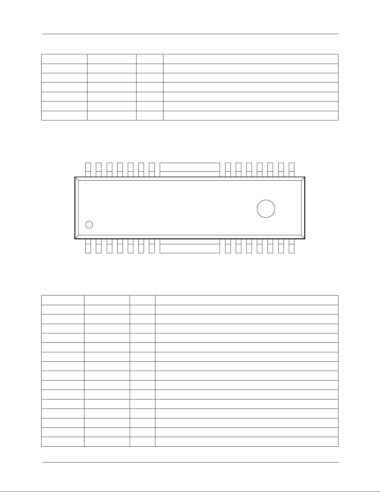
Pin Assignments (32SDIPH)
CTL
F/R
32 31 30 29 28 27 26 25 24 23 22 21 20 19 18 17
OUT2FGOUT1FGIN2FGIN1
CTL
TR
FG
GND
NC
REFVCTL
V
KA3080
U+
W+
W−
GND
RS
OUTUOUTVOUTWOUT
G
V−
V+
U−
Pin Definitions (32SDIPH)
Pine Number Pin Name I/O Pin Function Description
1 U+ I U+ Hall Signal Input
2 U- I U- Hall Signal Input
3 V+ I V+ Hall Signal Input
4 V- I V- Hall Signal Input
5 W+ I W+ Hall Signal Input
6 W- I W- Hall Signal Input
7 GND - Ground (Signal)
8 GND - Ground (Signal)
9 GND - Ground (Signal)
10 GND - Ground (Signal)
11 RS O Output Current Detection
12 G
13 U
14 V
15 W
16 V
17 V
OUT
OUT
OUT
OUT
CC2
CC1
18 CI - Phase Stabilization
19 I
20 V
21 V
LIM
CTL
REF
22 NC - No Connection
23 GND - Ground (Signal)
24 GND - Ground (Signal)
25 GND - Ground (Signal)
26 GND - Ground (Signal)
- Ground (Power)
OU Out
OV Out
OW Out
- Supply Voltage (Power)
- Supply Voltage(Signal)
I Current Limitation
I Voltage Control
I Voltage Control Reference
LIM
I
CC1
V
CI
16151413121110987654321
CC2
V
2
KA3080/KA3080D/KA3080DM
Pin Definitions (32-SDIPH)
(Continued)
Pine Number Pin Name I/O Pin Function Description
27 FG
28 FG
29 F G
30 F G
31 TR
32 F/R
IN1
IN2
OUT1
OUT2
CTL
CTL
I FG Amp. Input1
I FG Amp. Input2
O FG Amp. Output
O FG Comp. Output
I Troque Ripple Control
I Forward & Reverse Control
Pin Assignments (28-SSOPH)
OUT
OUT
W
V
28 27 26 25 24 23 22 21 20 19 18 17 16 15
OUT
OUT
G
U
NC
NC
RS
FIN
GND
W+
V−
W−
KA3080D
V+
U−
U+
FIN
CC2VCC1
V
CI
LIM
CTL
I
V
NC
REF
V
GND
IN1FGIN2
FG
OUT1
FG
Pin Definitions (28-SSOPH)
Pine Number Pin Name I/O Pin Function Description
1V
2V
CC2
CC1
3 CI - Phase Stabilization
4I
5V
6V
LIM
CTL
REF
7 NC - No Connection
8 GND - Ground (Signal)
9FG
10 FG
11 FG
12 FG
13 TR
14 FR
IN1
IN2
OUT1
OUT2
CTL
CTL
15 U+ I U+ Hall Signal Input
- Supply Voltage (Power)
- Supply Voltage (Signal)
I Current Limitation
I Voltage Control
I Voltage Control Reference
I FG Amp. Input 1
I FG Amp. Input 2
O FG Amp. Output
O FG Comp. Output
I Torque Ripple Control
I Forward & Reverse Control
OUT2
FG
1413121110987654321
CTLFRCTL
TR
3

KA3080/KA3080D/KA3080DM
Pin Definitions (28-SSOPH)
(Continued)
Pine Number Pin Name I/O Pin Function Description
16 U- I U- Hall Signal Input
17 V+ I V+ Hall Signal Input
18 V- I V- Hall Signal Input
19 W+ I W+ Hall Signal Input
20 W- I W- Hall Signal Input
21 GND - Ground (Signal)
22 RS O Output Current Detection
23 NC - No Connection
24 NC - No Connection
25 G
26 U
27 V
28 W
OUT
OUT
OUT
OUT
- Ground (Power)
OU Out
OV Out
OW Out
Internal Block Diagram (32-SDIPH)
CTL
F/R
32 31 30 29 28 27 24 23 22 21 20 19 18 17
CW & CCW
+
−
U+
TR
U−
OUT2FGIOUT1
CTL
FG
−
+
TSD
+
−−
V+
IN2FGIN1
FG
2.5V
−
+
+
V−
W+
W−
GND
26 25
LOGIC
GND
GND
GND
GND
GND
GND
GND
NC
RS
REF
V
−
+
OUT
G
CTL
LIM
V
I
1.25V
−
+
−
++
OUTVOUTWOUT
U
CC1
CI
V
16151413121110987654321
CC2
V
4

Internal Block Diagram (28-SSOPH)
KA3080/KA3080D/KA3080DM
OUT
OUT
W
V
1234567 8
CC2VCC1
V
OUT
OUT
U
G
NC
NC
RS
FIN
LOGIC
−
++
1.25V
LIM
I
+ −
CTL
REF
V
V
+ −
CI
2.5V
FIN
NC
GND
1.8k
GND
W−
W+
−
+
IN1
FG
−
+
IN2
FG
+
−
56k
91011121314
V−
−
+
TSD
OUT1FGOUT2
FG
V+
1516171819202122232425262728
−
+
CW&CCW
CTLFRCTL
TR
U+
U−
5

KA3080/KA3080D/KA3080DM
Equivalent Circuits (32-SDIPH: Ο, 28-SSOPH: (#))
Description Pin No. Internal Circuit
32-SDIPH
1, 2, 3
4, 5, 6
Hall Input
Output &
Current Detection
28-SSOPH
15, 16, 17
18, 19, 20
32-SDIPH
13, 14, 15, 11
28-SSOPH
26, 27, 28, 22
(15)
(17)
(19)
1
3
5
Vcc1
RS (0.5Ω)
16
(1) V
CC2
13
11
(22 Pin)
(26) U
14
2
4
6
OUT
12
(16)
(18)
(20)
(27) V
15
(25 Pin)
OUT
(28) W
OUT
Speed Control
(Current limitation)
6
32-SDIPH
19
28-SSOPH
4
(4)
Vcc1
19
 Loading...