

Fairchild Semiconductor MMBFJ309, MMBFJ310, J310, J309 Datasheet

Discrete POWER & Signal
Technologies
J309 / J310 / MMBFJ309 / MMBFJ310
J309
J310
G
S
D
TO-92
MMBFJ309
MMBFJ310
G
SOT-23
Mark: 6U / 6T
S
D
N-Channel RF Amplifier
This device is designed for VHF/UHF amplifier, oscillator and mixer
applications. As a common gate amplifier, 16 dB at 100 MHz and
12 dB at 450 MHz can be realized. Sourced from Process 92.
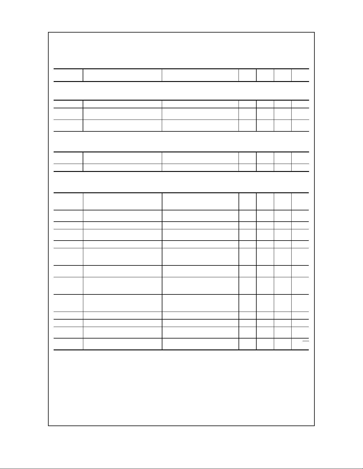
Absolute Maximum Ratings* TA = 25°C unless otherwise noted
Symbol Parameter Value Units
V
DS
V
GS
I
GF
TJ ,T
stg
*These ratings are limiting values above which the serviceability of any semiconductor device may be impaired.
NOTES:
1) These ratings are based on a maximum junction temperature of 150 degrees C.
2) These are steady state limits. The factory should be consulted on applications involving pulsed or low duty cycle operations.
Drain-Source Vol t age 25 V
Gate-Source Voltage - 25 V
Forward Gate Current 10 mA
Operating and Storage Junction Temperature Range -55 to +150
°
C
Thermal Characteristics TA = 25°C unless otherwise noted
Symbol Characteristic Max Units
J309 / J310 *MMBFJ309
P
D
R
θ
JC
R
θ
JA
*Device mounted on FR-4 PCB 1.6" X 1.6" X 0.06."
ã 1997 Fairchild Semiconductor Corporation
Total Device Dissipation
Derate above 25°C
Ther mal Resistance, Junction to Case 125
Thermal Resistance, Junction to Ambient 357 556
350
2.8
225
1.8
mW
mW/°C
C/W
°
C/W
°
(BR)
µ
)
µ
µ
µ
µ
µ
µ
µ
N-Channel RF Amplifier
(continued)
Electrical Characteristics TA = 25°C unless otherwise noted
Symbol Parameter Test Conditions Min Typ Max Units
OFF CHARACTERISTICS
V
GSS
I
GSS
V
GS(off
ON CHARACTERISTICS
I
DSS
V
GS(f)
SMALL SIGNAL CHARACTERISTICS
Re(y
is)
Re(y
os)
G
pg
Re(y
fs)
Re(y
ig)
g
fs
g
os
g
fg
g
og
C
dg
C
sg
NF Noise F igure VDS = 10 V, ID = 10 mA,
e
n
*Pulse Test: Pulse Width £ 300 ms, Duty Cycle £ 2.0%
Gate-Source Breakdown Volta g e
I
= - 1.0 µA, VDS = 0
G
Gate Reverse Current VGS = - 15 V, VDS = 0
V
= - 15 V, VDS = 0, TA = 125°C
GS
Gate-Source Cutoff Voltag e VDS = 10 V, ID = 1.0 nA
Zero-Gate Voltage Drain Current* VDS = 10 V, VGS = 0
J309
J310
J309
J310
- 25 V
- 1.0
- 1.0
- 1.0
- 2.0
12
- 4.0
- 6.5VV
3060mA
24
mA
Gate-Source Forward Volt age VDS = 0, IG = 1.0 mA 1.0 V
Common-Source Input Conductance VDS = 10, ID = 10 mA, f = 100 MHz
Common-Source Output
J309
J310
0.7
0.5
VDS = 10, ID = 10 mA, f = 100 MHz 0.25 mmhos
mmhos
mmhos
Conductance
Common-Gate Power Gain VDS = 10, ID = 10 mA, f = 100 MHz 16 dB
Common-Source Forward
VDS = 10, ID = 10 mA, f = 100 MHz 12 mmhos
Transconductance
Common-Gate Input Conductance VDS = 10, ID = 10 mA, f = 100 MHz 12 mmhos
Common-Source Forward
Transconductance
Common-Source Output
VDS = 10, ID = 10 mA, f = 1.0 kHz
J309
J310
10,000
8000
20,000
18,000
VDS = 10, ID = 10 mA, f = 1.0 kHz 150
mhos
mhos
mhos
Conductance
Common-Gate Forward Conductance VDS = 10, ID = 10 mA, f = 1.0 kHz
J309
J310
13,000
12,000
mhos
mhos
Common-Gate Output Conductance VDS = 10, ID = 10 mA, f = 1.0 kHz
J309
J310
100
150
mhos
mhos
Drain-Gate Capacitance VDS = 0, VGS = - 10, f = 1.0 MHz 2.0 2.5 pF
Source-Gate Capacitance VDS = 0, VGS = - 10, f = 1.0 MHz 4.1 5.0 pF
3.0 dB
f = 450 MHz
Equivalent Short-Circuit Input
Noise Voltage
VDS = 10 V, ID = 10 mA,
f = 100 Hz
6.0
nV/ÖHz
J309 / J310 / MMBFJ309 / MMBFJ310
nA
A
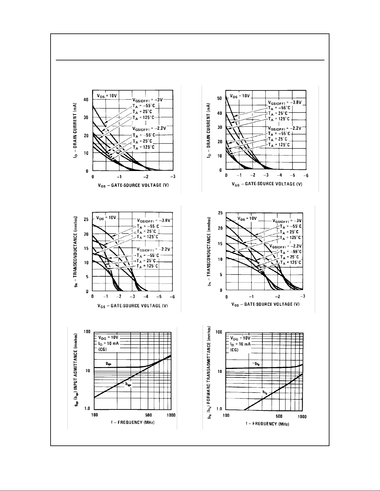
Typical Characteristics
J309 / J310 / MMBFJ309 / MMBFJ310
N-Channel RF Amplifier
(continued)
Transfer Characteristics
Transfer Characteristics
Transfer Characteristics
Transfer Characteristics
Input Admittance
Forward Transadmittance
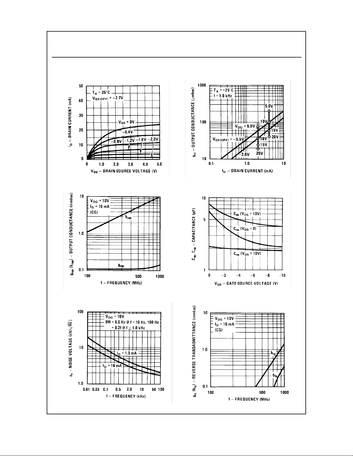
Typical Characteristics (continued)
Common Drain-Source
J309 / J310 / MMBFJ309 / MMBFJ310
N-Channel RF Amplifier
(continued)
Output Conductance vs.
Drain Current
Output Admittance
Noise Voltage vs. Frequency
Capacitance vs. Voltage
Reverse Transadmittance
 Loading...