

Fairchild Semiconductor FDP7030BL, FDB7030BL Datasheet
FDP7030BL/FDB7030BL
N-Channel Logic Level PowerTrench
General Description Features
TM
MOSFET
July 1998
This N-Channel Logic Level MOSFET has been designed
specifically to improve the overall efficiency of DC/DC
converters using either synchronous or conventional
switching PWM controllers.
These MOSFETs feature faster switching and lower gate
charge than other MOSFETs with comparable R
specifications.
DS(on)
The result is a MOSFET that is easy and safer to drive (even
at very high frequencies), and DC/DC power supply designs
with higher overall efficiency.
60 A, 30 V. R
R
= 0.009 Ω @ V
DS(ON)
= 0.0120 Ω @ V
DS(ON)
= 10 V,
GS
= 4.5 V.
GS
Critical DC electrical parameters specified at elevated
temperature.
Rugged internal source-drain diode can eliminate the need
for an external Zener diode transient suppressor.
High performance trench technology for extremely low
R
.
DS(ON)
175°C maximum junction temperature rating.
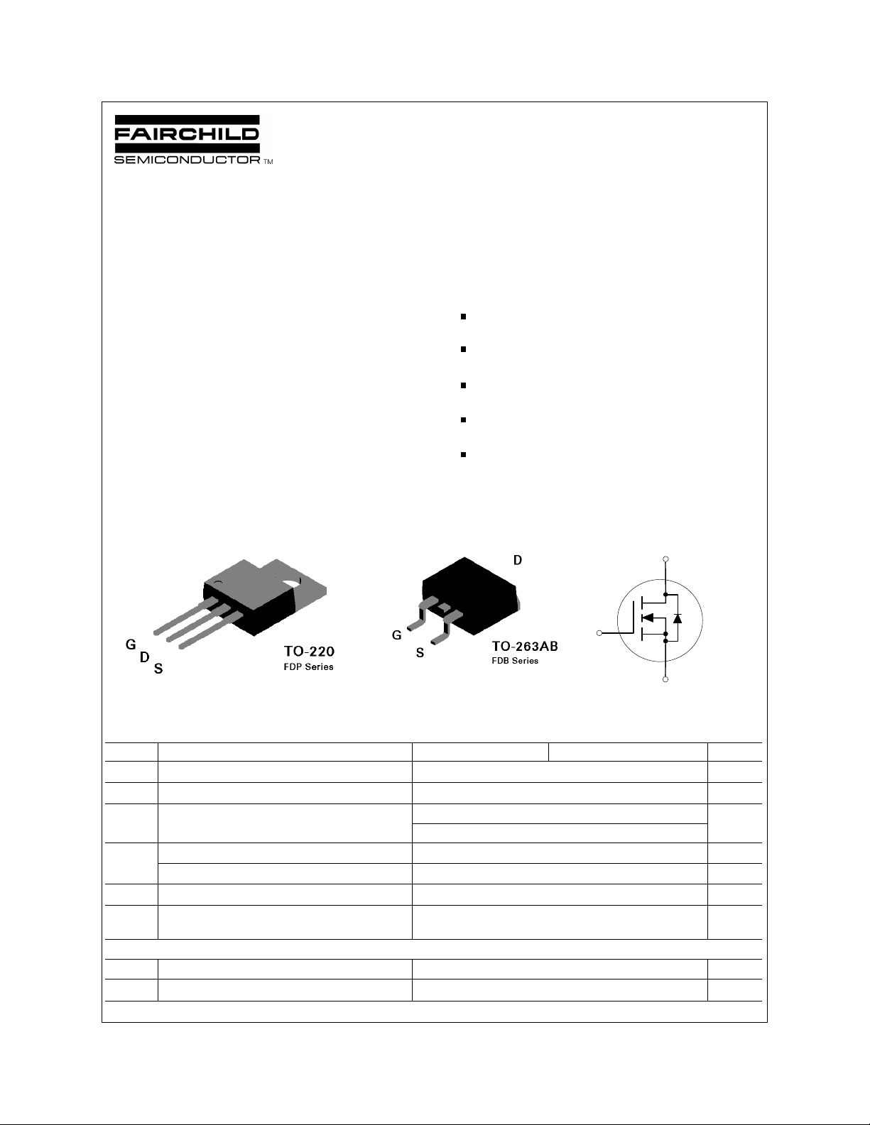
_________________________________________________________________________________
D
G
S
Absolute Maximum Ratings T
= 25°C unless otherwise noted
C
Symbol Parameter FDP7030BL FDB7030BL Units
V
DSS
V
GSS
I
D
Drain-Source Voltage 30 V
Gate-Source Voltage ±20 V
Drain Current - Continuous (Note 1) 60 A
- Pulsed (Note 1) 180
P
D
Total Power Dissipation @ TC = 25°C
65 W
Derate above 25°C 0.43 W/°C
TJ,T
T
L
Operating and Storage Temperature Range -65 to 175 °C
STG
Maximum lead temperature for soldering purposes,
275 °C
1/8" from case for 5 seconds
THERMAL CHARACTERISTICS
R
JC
θ
R
JA
θ
© 1998 Fairchild Semiconductor Corporation
Thermal Resistance, Junction-to-Case 2.3 °C/W
Thermal Resistance, Junction-to-Ambient 62.5 °C/W
FDP7030BL Rev.C
Electrical Characteristics (T
= 25°C unless otherwise noted)
C
Symbol Parameter Conditions Min Typ Max Unit
DRAIN-SOURCE AVALANCHE RATINGS (Note 1)
W
DSS
I
AR
Single Pulse Drain-Source Avalanche Energy VDD = 15 V, ID = 60 A 220 mJ
Maximum Drain-Source Avalanche Current 60 A
OFF CHARACTERISTICS
BV
∆BV
I
DSS
I
GSSF
I
GSSR
DSS
DSS
Drain-Source Breakdown Voltage VGS = 0 V, ID = 250 µA 30 V
Breakdown Voltage Temp. Coefficient
/∆T
J
Zero Gate Voltage Drain Current
ID = 250 µA, Referenced to 25 oC
VDS = 24 V, V
GS
= 0 V
22
1 µA
Gate - Body Leakage, Forward VGS = 20 V, VDS = 0 V 100 nA
Gate - Body Leakage, Reverse
VGS = -20 V, VDS = 0 V
mV/oC
-100 nA
ON CHARACTERISTICS (Note 2)
V
∆V
R
GS(th)
GS(th)
DS(ON)
Gate Threshold Voltage VDS = VGS, ID = 250 µA 1 1.5 3 V
Gate Threshold Voltage Temp.Coefficient
/∆T
J
Static Drain-Source On-Resistance
ID = 250 µA, Referenced to 25 oC
VGS = 10 V, ID = 30 A
-5
0.0073 0.009
mV/oC
TJ = 125°C 0.011 0.018
0.01 0.012
55 S
I
g
D(on)
FS
VGS = 4.5 V, ID = 25 A
On-State Drain Current VGS = 10 V, VDS = 10 V 60 A
Forward Transconductance
VDS = 10 V, ID = 30 A
DYNAMIC CHARACTERISTICS
C
iss
C
oss
C
rss
Input Capacitance VDS = 15 V, VGS = 0 V,
Output Capacitance 480 pF
f = 1.0 MHz
Reverse Transfer Capacitance 200 pF
2400 pF
SWITCHING CHARACTERISTICS (Note 1)
t
t
t
t
Q
Q
Q
D(on)
r
D(off)
f
g
gs
gd
Turn - On Delay Time VDD = 10 V, ID = 1 A,
Turn - On Rise Time 14 26 nS
VGS = 10 V, R
GEN
= 6 Ω
13 24 nS
Turn - Off Delay Time 43 70 nS
Turn - Off Fall Time 15 27 nS
Total Gate Charge
Gate-Source Charge 7 nC
V
= 15 V , ID = 30 A
DS
V
= 5 V
GS
23 33 nC
Gate-Drain Charge 11 nC
DRAIN-SOURCE DIODE CHARACTERISTICS
I
S
Maximum Continuous Drain-Source Diode Forward Current (Note 1) 60 A
ISM Maximum Pulsed Drain-Source Diode Forward Current (Note 1) 180 A
V
SD
t
rr
Irr Reverse Recovery Current 0.79 5 A
Notes
1. Pulse Test: Pulse Width < 300 µs, Duty Cycle < 2.0%.
Drain-Source Diode Forward Voltage
VGS = 0 V, IS = 30 A (Note1)
Reverse Recovery Time VGS = 0 V, IF = 30 A
dIF/dt = 100 A/µs
1 1.3 V
22 50 ns
Ω
FDP7030BL Rev.C
 Loading...