

Fairchild Semiconductor FDP42AN15A0, FDB42AN15A0 Datasheet
FDP42AN15A0 / FDB42AN15A0
N-Channel PowerTrench® MOSFET
150V, 35A, 42mΩ
FDP42AN15A0 / FDB42AN15A0
September 2002
Features
•r
•Q
• Low Miller Charge
• Low Qrr Body Diode
• UIS Capability (Single Pulse and Repetitive Pulse)
• Qualified to AEC Q101
Formerly developmental type 82864
MOSFET Maximum Ratings T
= 36mΩ (Typ.), V
DS(ON)
(tot) = 33nC (Typ.), V
g
GATE
SOURCE
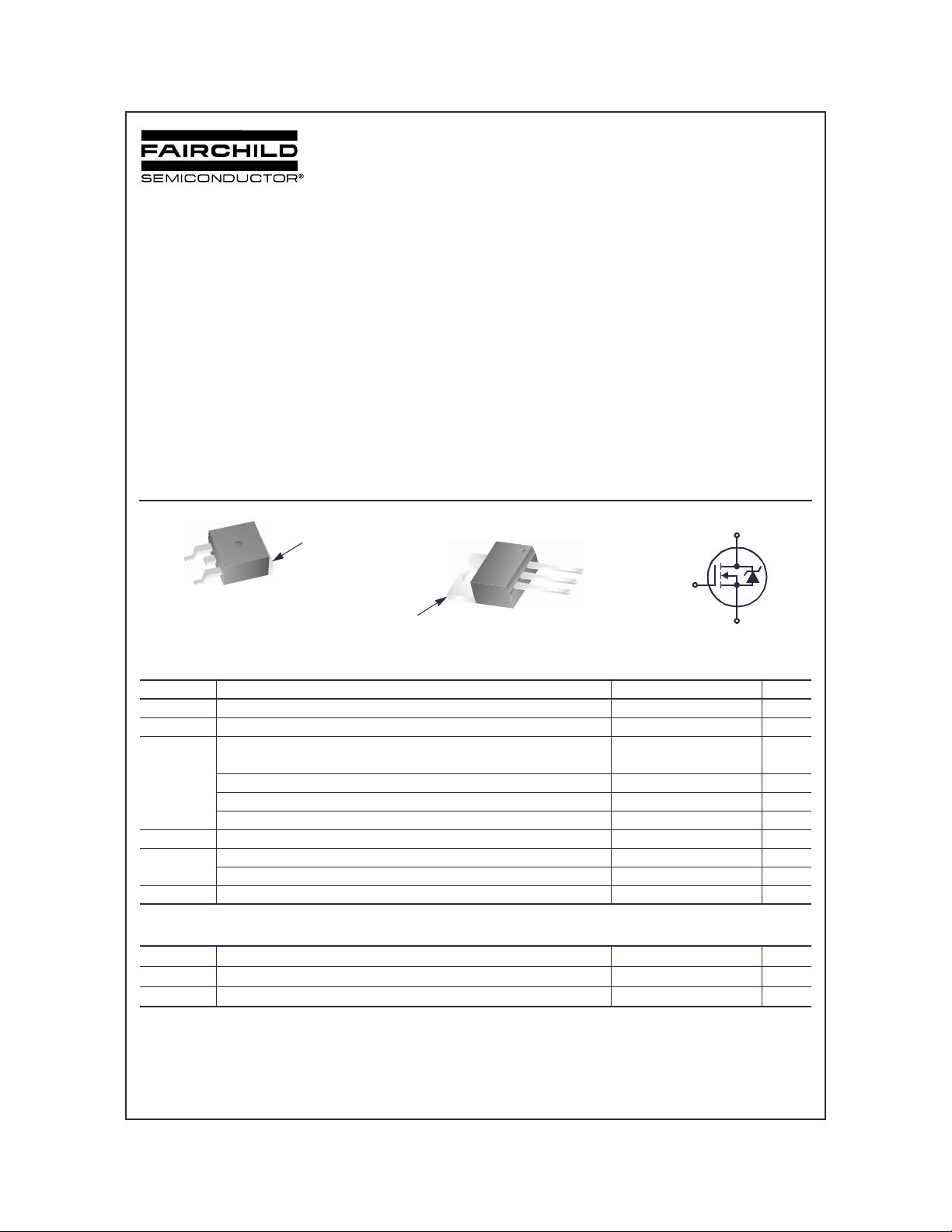
TO-263AB
FDB SERIES
= 10V, ID = 12A
GS
= 10V
GS
DRAIN
(FLANGE)
DRAIN
(FLANGE)
= 25°C unless otherwise noted
C
Applications
• DC/D C C onverter s an d Of f-line UPS
• Distributed P ower Arc hitectures and VRMs
• Primary Switch for 24V and 48V Syst ems
• High Voltage Synchronous Rectifier
• Direct Injection / Diesel Injection Systems
• 42V Automotiv e Load Control
• Elec tr on ic Valve Train Sys tems
D
SOURCE
DRAIN
GATE
TO-220AB
FDP SERIES
G
S
Symbol Parameter Ratings Units
V
DSS
V
GS
Drain to Source Voltage 150 V
Gate to Source Voltage ±20 V
Drain Curr e nt
Continuous (T
I
D
Continuous (T
Continuous (T
= 25oC, VGS = 10V)
C
= 100oC, VGS = 10V) 24
C
= 25oC, VGS = 10V, with R
amb
= 43oC/W) 5 A
θJA
35 A
Pulsed Figure 4 A
E
AS
P
D
, T
T
J
STG
Single Pulse Avalanche Energy (Note 1) 90 mJ
Power dissipation 150 W
o
Derate above 25
C1.00W/
Operating and Storage Temperature -55 to 175
o
C
o
C
Thermal Characteristi cs
R
θJC
R
θJA
R
θJA
This product has been designed to meet the extreme test conditions and environment demanded by the automotive
All Fairchild Semiconductor products are manufactured, assembled and tested under ISO9000 and QS9000 quality
©2002 Fairchild Semiconductor Corporation
Thermal Resistance Junction to Case TO-220,TO-263 1.0
Thermal Resistance Junction to Ambient TO-220,TO-263 62
Thermal Resistance Junction to Ambient TO-263, 1in2 copper pad ar ea 43
industry. For a copy of the requirements, see AEC Q101 at: http://www.aecouncil.com/
Reliability data can be found at: http://www.fairchildsemi.com/products/discrete/reliability/index.html.
systems certification.
FDP42AN15A0 / FDB42AN15A0 Rev. C
o
C/W
o
C/W
o
C/W
Package Marking and Ordering Information
Device Marking Device Package Reel Size Tape Width Quantity
FDB42AN15A0 FDB42AN15A0 TO-263AB 330mm 24mm 800 units
FDP42AN15A0 FDP42AN15A0 TO-220AB Tube N/A 50 units
FDP42AN15A0 / FDB42AN15A0
Electrical Characteristics
TC = 25°C unless otherwise noted
Symbol Parameter Test Con ditions Min Typ Max Units
Off Characteristics
B
I
DSS
I
GSS
VDSS
Drain to Sou r c e Br ea k down Volt ag e ID = 250µA, VGS = 0V 150 - - V
V
= 120V - - 1
Zero Gate Voltage Drain Current
DS
= 0V TC = 150oC- -250
V
GS
Gate to Source Leakage Current VGS = ±20V - - ±100 nA
On Characteristics
V
GS(TH)
r
DS(ON)
Gate to Source Threshold Voltage VGS = VDS, ID = 250µA2-4V
= 12A, VGS = 10V - 0.036 0.042
I
D
I
= 6A, VGS = 6V - 0.040 0.060
Drain to S ou r c e On Re si st ance
D
= 12A, VGS = 10V,
I
D
T
= 175oC
J
- 0.090 0.107
Dynamic Characteristics
C
C
C
Q
Q
Q
Q
Q
ISS
OSS
RSS
g(TOT)
g(TH)
gs
gs2
gd
Input Capacitance
Output Capacitanc e - 225 - pF
Reverse Transfer Capacitance - 45 - pF
= 25V, VGS = 0V,
V
DS
f = 1MHz
Total Gate Charge at 10V VGS = 0V to 10V
Threshold Gate Charge VGS = 0V to 2V - 4.2 5.4 nC
Gate to Source Gate Charg e - 9.5 - nC
Gate Charge Threshold to Plateau - 5.3 - nC
V
DD
I
= 12A
D
I
= 1.0m A
g
= 75V
Gate to Drain “Miller” Charge - 6.9 - nC
- 2150 - pF
30 39 nC
µA
Ω
Switching Characteristics
t
ON
t
d(ON)
t
r
t
d(OFF)
t
f
t
OFF
Turn-On Time
Turn-On Delay Time - 11 - ns
Rise Time - 19 - ns
Turn-Off D elay Time - 27 - ns
Fall Time - 23 - ns
Turn-Off Time - - 74 ns
(VGS = 10V)
Drain-Source Diode Characteristics
V
SD
t
rr
Q
RR
Notes:
1: Starting TJ = 25°C, L = 0.2mH, IAS = 30A.
©2002 Fairchild Semiconductor Corporation
Source to Drain Diode Voltage
Reverse Recovery Time ISD = 12A, dISD/dt = 100A/µs- -82ns
Reverse Recovered Charge ISD = 12A, dISD/dt = 100A/µs - - 204 nC
- - 46 ns
V
= 75V, ID = 12A
DD
V
= 10V, RGS = 7.5Ω
GS
I
= 12A - - 1.2 5 V
SD
= 6A - - 1.0 V
I
SD
FDP42AN15A0 / FDB42AN15A0 Rev. C
FDP42AN15A0 / FDB42AN15A0
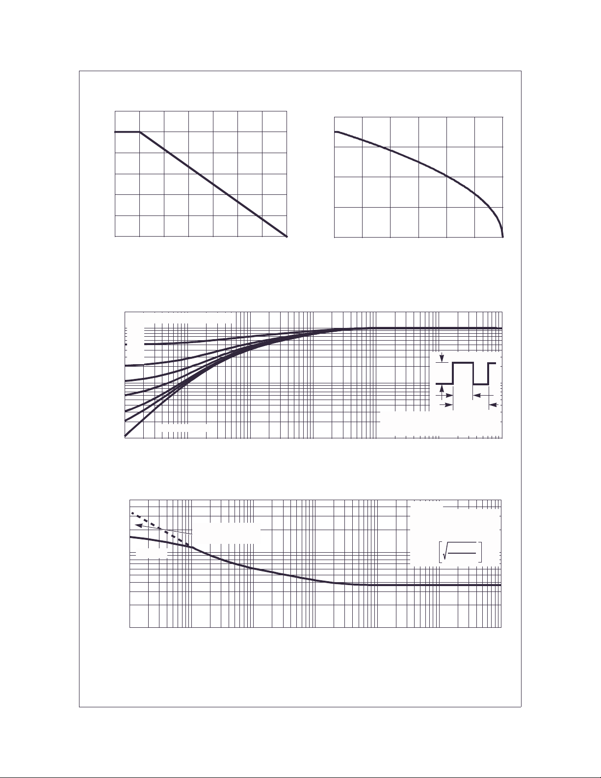
Typical Characteristics T
= 25°C unless otherwise noted
C
1.2
1.0
0.8
0.6
0.4
0.2
POWER DISSIPATION MULTIPLIER
0
0255075100 175
125
TC, CASE TEMPERATURE (oC)
Figure 1. Normalized Power Dissipation vs
Ambient Temperature
2
DUTY CYCLE - DESCENDING ORDER
0.5
1
0.2
0.1
0.05
0.02
0.01
0.1
, NORMALIZED
θJC
Z
THERMAL IMPEDANCE
0.01
-5
10
SINGLE PULSE
-4
10
10
40
30
20
, DRAIN CURRENT (A)
D
10
I
150
0
25 50 75 100 125 150 175
Figure 2. Maximum Continuous Drain Curr ent vs
-3
t, RECTANGULAR PULSE DURATION (s)
-2
10
TC, CASE TEMPERATURE (oC)
Case Temperature
P
DM
NOTES:
DUTY FACTOR: D = t1/t
PEAK TJ = PDM x Z
-1
10
θJC
10
x R
0
t
1
t
2
2
+ T
θJC
C
1
10
500
VGS = 10V
100
, PEAK CURRENT (A)
DM
I
10
-5
10
©2002 Fairchild Semiconductor Corporation
Figure 3. Normalized Maximum Transient Thermal Impedance
TC = 25oC
FOR TEMPERATURES
TRANSCONDUCTANCE
MAY LIMIT CURRENT
IN THIS REGION
ABOVE 25oC DERATE PEAK
CURRENT AS FOLLOWS:
I = I
-4
10
-3
10
-2
10
-1
10
t, PULSE WIDTH (s)
Figure 4. Peak Current Capability
175 - T
25
10
FDP42AN15A0 / FDB42AN15A0 Rev. C
C
150
0
10
1
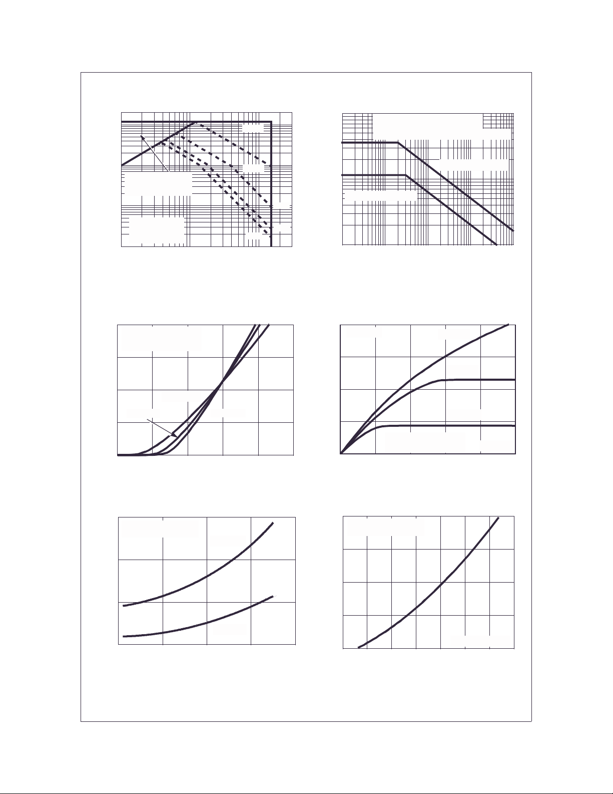
FDP42AN15A0 / FDB42AN15A0
Typical Characteristics T
200
100
10
OPERATION IN THIS
AREA MAY BE
LIMITED BY r
1
, DRAIN CURRENT (A)
D
I
SINGLE PULSE
TJ = MAX RATED
TC = 25oC
0.1
1 10 100 300
DS(ON)
VDS, DRAIN TO SOURCE VOLTAGE (V)
= 25°C unless otherwise noted
C
10µs
100µs
DC
Figure 5. Forward Bias Safe Operating Area
80
PULSE DURATION = 80µs
DUTY CYCLE = 0.5% MAX
V
= 15V
DD
60
1ms
10ms
100
10
, AVALANCHE CURRENT (A)
AS
I
1
0.001 0.01 0.1 1 10
If R = 0
tAV = (L)(IAS)/(1.3*RATED BV
If R ≠ 0
t
= (L/R)ln[(IAS*R)/(1.3*RATED BV
AV
STARTING TJ = 150oC
tAV, TIME IN AVALANCHE (ms)
- VDD)
DSS
- VDD) +1]
DSS
STARTING TJ = 25oC
NOTE: Refer to Fairchild Application Notes AN7514 and AN7515
Figure 6. Unclamped Inductive Switching
Capability
80
VGS = 20V
60
VGS = 10V
VGS = 6V
40
TJ = 25oC
, DRAIN CURRENT (A)
D
I
20
0
345678
TJ = 175oC
TJ = -55oC
VGS, GATE TO SOURCE VOLTAGE (V)
40
, DRAIN CURRENT (A)
D
I
20
PULSE DURATION = 80µs
0
012345
DUTY CYCLE = 0.5% MAX
VDS, DRAIN TO SOURCE VOLTAGE (V)
Figure 7. Transfer Characteristics Figure 8. Saturation Characteristics
50
PULSE DURATION = 80µs
DUTY CYCLE = 0.5% MAX
45
40
DRAIN TO SOURCE ON RESISTANCE(mΩ)
35
0 10203040
ID, DRAIN CURRENT (A)
VGS = 6V
VGS = 10V
2.5
PULSE DURATION = 80µs
DUTY CYCLE = 0.5% MAX
2.0
1.5
ON RESISTANCE
1.0
NORMALIZED DRAIN TO SOURCE
0.5
-80 -40 0 40 80 120 160 200
TJ, JUNCTION TEMPERATURE (oC)
VGS = 5V
TC = 25oC
VGS = 10V, ID =12A
Figure 9. Drain to So urce On Resistanc e v s Drai n
Current
©2002 Fairchild Semiconductor Corporation
Figure 10. Normalized Drain to Source On
Resistance vs Junction Temperature
FDP42AN15A0 / FDB42AN15A0 Rev. C
 Loading...