

Fairchild Semiconductor FDN340P Datasheet
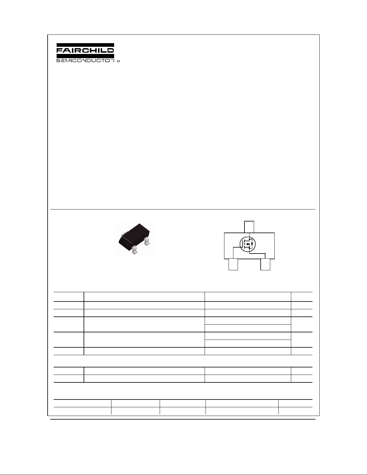
FDN340P
FDN340P
Single P-Channel , Logic Level, PowerTrench MOSFET
December 1999
General Description
This P-Channel Logic Level MOSFET is produced
using Fairchild Semiconductor advanced Power Trench
process that has been especially tailored to minimize
the on-state resistance and yet maintain low gate
charge for superior switching performance.
These devices are well suited for portable electronics
applications: Load switching and power management,
battery charging circuits, and DC/DC conversion.
D
340
SuperSOT -3
TM
S
G
Features
–2 A, 20 V. R
• Low gate charge (8nC typical).
• High performance trench technology for extremely
low R
DS(ON)
.
• High power version of industry Standard SOT-23
package. Identical pin-out to SOT-23 with 30%
higher power handling capability.
= 0.07 Ω @ VGS = –4.5 V
DS(ON)
R
= 0.11 Ω @ VGS = –2.5 V.
DS(ON)
R
= 0.210 Ω @ VGS = –1.8 V.
DS(ON)
D
SG
Absolute Maximum Ratings T
=25oC unless otherwise noted
A
Symbol Parameter Ratings Units
V
DSS
V
GSS
I
D
P
D
TJ, T
STG
Drain-Source Voltage –20 V
Gate-Source Voltage ±8 V
Drain Current – Continuous (Note 1a) –2 A
– Pulsed –10
Power Dissipation for Single Operation (Note 1a) 0.5
(Note 1b)
0.46
Operating and Storage Junction Temperature Range -55 to +150 °C
Thermal Characteristics
R
θJA
R
θJC
Thermal Resistance, Junction-to-Ambient (Note 1a) 250
Thermal Resistance, Junction-to-Case (Note 1) 75
°C/W
°C/W
Package Marking and Ordering Information
Device Marking Device Reel Size Tape width Quantity
340 FDN340P 7’’ 8mm 3000 units
1999 Fairchild Semiconductor Corporation
FDN340P Rev C (W)
W
Electrical Characteristics T
= 25°C unless otherwise noted
A
Symbol Parameter Test Conditions Min Typ Max Units
Off Characteristics
BV
DSS
∆BVDSS
∆T
J
I
DSS
I
GSSF
I
GSSR
Drain–Source Breakdown Voltage
Breakdown Voltage Temperature
Coefficient
Zero Gate Voltage Drain Current
Gate–Body Leakage, Forward VGS = 8 V, VDS = 0 V 100 nA
Gate–Body Leakage, Reverse VGS = –8 V VDS = 0 V –100 nA
VGS = 0 V, ID = –250 µA
ID = –250 µA,Referenced to 25°C
–20 V
–15
VDS = –16 V, VGS = 0 V –1
TJ=55°C
–10
mV/°C
µA
On Characteristics (Note 2)
V
GS(th)
∆VGS( th)
∆T
R
DS(on)
I
D(on)
g
FS
Gate Threshold Voltage VDS = VGS, ID = –250 µA –0.4 –0.9 –1.5 V
Gate Threshold Voltage
Temperature Coefficient
J
Static Drain–Source
On–Resistance
ID = –250 µA,Referenced to 25°C
VGS = –4.5 V, ID = –2 A
TJ=125°C
VGS= –2.5 V, ID = –1.7A,
2.7 mV/°C
0.052 0.07
0.075 0.12
0.078 0.11
VGS= –1.8 V, ID = –1.2 A,
On–State Drain Current VGS = –4.5 V, VDS = –5 V –5 A
Forward Transconductance VDS = –4.5 V, ID = –2 A 8 S
0.21
Dynamic Characteristics
C
iss
C
oss
C
rss
Input Capacitance 600 pF
Output Capacitance 175 pF
Reverse Transfer Capacitance
VDS = –10 V, V
f = 1.0 MHz
GS
= 0 V,
80 pF
FDN340P
Ω
Switching Characteristics (Note 2)
t
t
t
t
Q
Q
Q
d(on)
r
d(off)
f
g
gs
gd
Turn–On Delay Time 6 12 ns
Turn–On Rise Time 9 18 ns
VDD = –5 V, ID = –0.5 A,
VGS = –4.5 V, R
GEN
= 6 Ω
Turn–Off Delay Time 31 50 ns
Turn–Off Fall Time
Total Gate Charge 8 11 nC
Gate–Source Charge 1.3 nC
VDS = –10 V, ID = –2 A,
VGS = –4.5 V
Gate–Drain Charge
26 42 ns
2.2 nC
Drain–Source Diode Characteristics and Maximum Ratings
I
S
V
SD
Notes:
1. R
θJA
the drain pins. R
Scale 1 : 1 on letter size paper
2. Pulse Test: Pulse Width < 300µs, Duty Cycle < 2.0%
Maximum Continuous Drain–Source Diode Forward Current –0.42 A
Drain–Source Diode Forward
Voltage
is the sum of the junction-to-case and case-to-ambient thermal resistance where the case thermal reference is defined as the solder mounting surface of
is guaranteed by design while R
θJC
a. 250°C/W when mounted on a
0.02in2 pad of 2 oz copper
is determined by the user's board design.
θCA
VGS = 0 V, IS = –0.42 A (Note ) –0.7 –1.2 V
b. 270°C/W when mounted on a
.001 in2 pad of 2 oz copper
FDN340P Rev C (W)
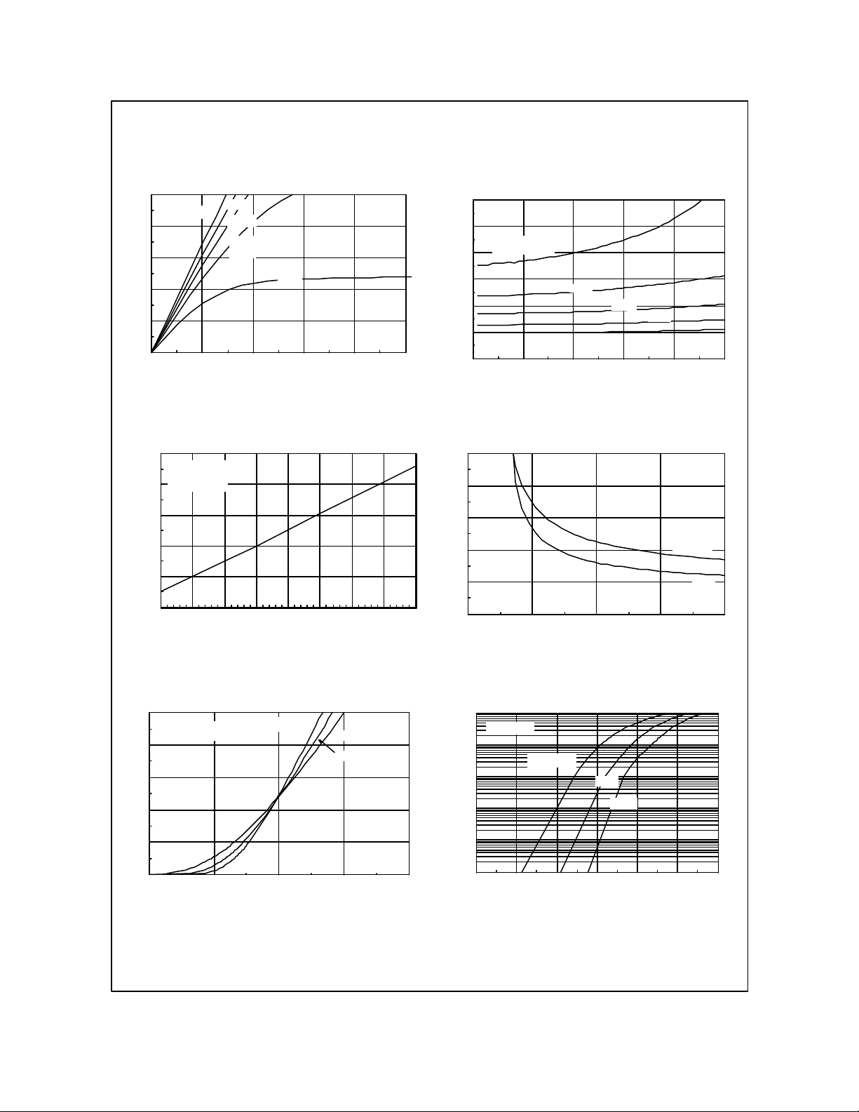
Typical Characteristics
FDN340P
10
8
V = -4.5V
GS
-3.5V
-3.0V
-2.5V
6
-2.0V
4
2
D
- I , DRAIN-SOURCE CURRENT (A)
0
0 0 1 1 2 2
-V , DRAIN-SOURCE VOLTAGE (V)
DS
2
1.8
V = -2.5 V
1.6
1.4
1.2
DS(on)
R , NORMALIZED
DRAIN-SOURCE ON-RESISTANCE
0.8
GS
-3.0V
-3.5V
1
0 2 4 6 8 10
- I , DRAIN CURRENT (A)
D
Figure 1. On-Region Characteristics. Figure 2. On-Resistance Variation with
Drain Current and Gate Voltage.
2
I = -2A
D
V = -4.5V
GS
1
1
1
DS(ON)
DRAIN-SOURCE ON-RESISTANCE
R , NORMALIZED
1
1
-50 -25 0 25 50 75 100 125 150
T , JUNCTION TEMPERATURE (°C)
J
0.2
0.16
0.12
0.08
0.04
DS(ON)
R , ON-RESISTANCE (OHM)
0
1 2 3 4 5
V , GATE TO SOURCE VOLTAGE (V)
GS
-4.0V
-4.5V
I = -1A
D
T = 125°C
A
25°C
Figure 3. On-Resistance Variation
withTemperature.
10
V = -5V
DS
8
6
4
D
- I , DRAIN CURRENT (A)
2
0
1 2 2 3 3
-V , GATE TO SOURCE VOLTAGE (V)
GS
T = -55°C
J
125°C
25°C
Figure 4. On-Resistance Variation with
Gate-to-Source Voltage.
10
V = 0V
GS
1
0.1
0.01
0.001
S
-I , REVERSE DRAIN CURRENT (A)
0.0001
0 0.2 0.4 0.6 0.8 1 1.2
T = 125°C
J
25°C
-55°C
-V , BODY DIODE FORWARD VOLTAGE (V)
SD
Figure 5. Transfer Characteristics. Figure 6. Body Diode Forward Voltage Variation
with Source Current and Temperature.
FDN340P Rev C (W)
 Loading...