

Fairchild Semiconductor FDN335N Datasheet
FDN335N
N-Channel 2.5V Specified PowerTrenchTM MOSFET
FDN335N
April 1999
General Description
This N-Channel 2.5V specified MOSFET is produced
using Fairchild Semiconductor's advanced PowerTrench
process that has been especially tailored to minimize the
on-state resistance and yet maintain low gate charge for
superior switching performance.
Applications
• DC/DC converter
• Load switch
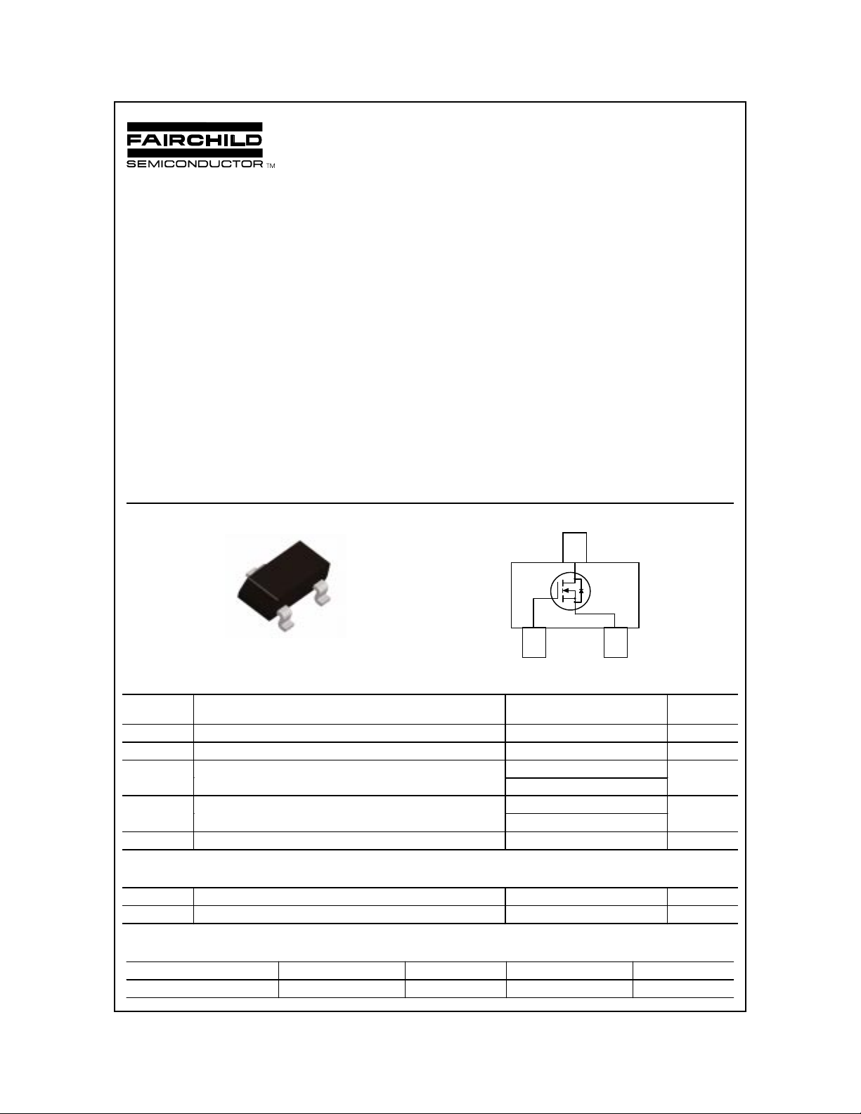
D
S
SuperSOT -3
TM
G
Features
• 1.7 A, 20 V. R
R
= 0.07 Ω @ V
DS(ON)
= 0.100 Ω @ V
DS(ON)
= 4.5 V
GS
= 2.5 V.
GS
• Low gate charge (3.5nC typical).
• High performance trench technology for extremely
low R
DS(ON)
.
• High power and current handling capability .
D
GS
Absolute Maximum Ratings
TA = 25°C unless otherwise noted
Symbol Parameter Ratings Units
V
DSS
V
GSS
I
D
P
D
TJ, T
stg
Drain-Source Voltage 20 V
Gate-Source Voltage
(Note 1a)
(Note 1a)
(Note 1b)
Drain Current - Continuous
- Pulsed 8
Power Dissipation for Single Operation
Operating and Storage Junction Temperature Range -55 to +150
8
±
1.7 A
0.5 W
0.46
Thermal Characteristics
R
JA
θ
R
JC
θ
Thermal Resistance, Junction-to-Ambi ent
Thermal Resistance, Junction-to-Case
(Note 1a)
(Note 1)
250
75
Package Outlines and Ordering Information
Device Marking Device Reel Size Tape Width Quantity
335 FDN335N 7’’ 8mm 3000 units
1999 Fairchild Semiconductor Corporation
V
C
°
C/W
°
C/W
°
FDN335N Rev. C
FDN335N
Electrical Characteristics
Symbol
Off Characteristics
BV
DSS
DSS
BV
∆
T
J
∆
I
DSS
I
GSSF
I
GSSR
Drain-Source Breakdown Voltage VGS = 0 V, ID = 250 µA20 V
Breakdown Voltage Temperature
Coefficient
Zero Gate Voltage Drain Current VDS = 16 V, VGS = 0 V 1
Gate-Body Leakage Current,
Forward
Gate-Body Leakage Current,
Reverse
On Characteristics
V
GS(th)
GS(th)
V
∆
T
J
∆
R
DS(ON)
I
D(on)
g
FS
Gate Threshold Voltage VDS = VGS, ID = 250 µA 0.4 0.9 1.5 V
Gate Threshold Voltage
Temperature Coefficient
Static Drain-Source
On-Resistance
On-State Drain Current VGS = 4.5 V, VDS = 5 V 8 A
Forward Transconductance VDS = 5 V, ID = 1.5 A 7 S
Dynamic Characteristics
C
iss
C
oss
C
rss
Input Capacitance 310 pF
Output Capacitance 80 pF
Reverse Transfer Capacitance
Parameter Test Conditions Min Typ Max Units
(Note 2)
TA = 25°C unless otherwise noted
ID = 250 µA,Referenced to 25°C14mV/
C
°
A
µ
VGS = 8 V, VDS = 0 V 100 nA
VGS = -8 V, VDS = 0 V -100 nA
ID = 250 µA,Referenced to 25°C-3mV/
VGS = 4.5 V, ID = 1.7 A
V
= 4.5 V, ID = 1.7 A,TJ = 125°C
GS
V
= 2.5 V, ID = 1.5 A
GS
V
= 10 V, VGS = 0 V,
DS
0.055
0.079
0.078
0.070
0.120
0.100
C
°
Ω
f = 1.0 MHz
40 pF
(Note 2)
Switching Characteristics
t
d(on)
t
r
t
d(off)
t
f
Q
Q
Q
g
gs
gd
Turn-On Delay Time 5 15 ns
Turn-On Rise Time 8.5 17 ns
Turn-Off Delay Time 11 20 ns
Turn-Off Fall Time
Total Gate Charge 3.5 5 nC
Gate-Source Charge 0.55 nC
Gate-Drain Charge
V
= 10 V, ID = 1 A,
DD
V
= 4.5 V, R
GS
V
= 10 V, ID = 1.7 A,
DS
V
= 4.5 V,
GS
GEN
= 6
Drain-Source Diode Characteristics and Maximum Ratings
I
S
V
SD
Notes:
1: R
θJA
surface of the drain pins. R
Scale 1 : 1 on letter size paper
2: Pulse Test: Pulse Width ≤ 300 µs, Duty Cycle ≤ 2.0%
Maximum Continuous Drain-Source Diode Forward Current 0.42 A
Drain-Source Diode Forward
VGS = 0 V, IS = 0.42 A
Voltage
is the sum of the junction-to-case and case-to-ambient thermal resistance where the case thermal reference is defined as the solder mounting
a) 250°C/W when
mounted on a 0.02 in
Pad of 2 oz. Cu.
is guaranteed by design while R
θJC
2
is determined by the user's board design.
θCA
b) 270°C/W when mounted
on a minimum pad.
Ω
(Note 2)
310ns
0.95 nC
0.7 1.2 V
FDN335N Rev. C
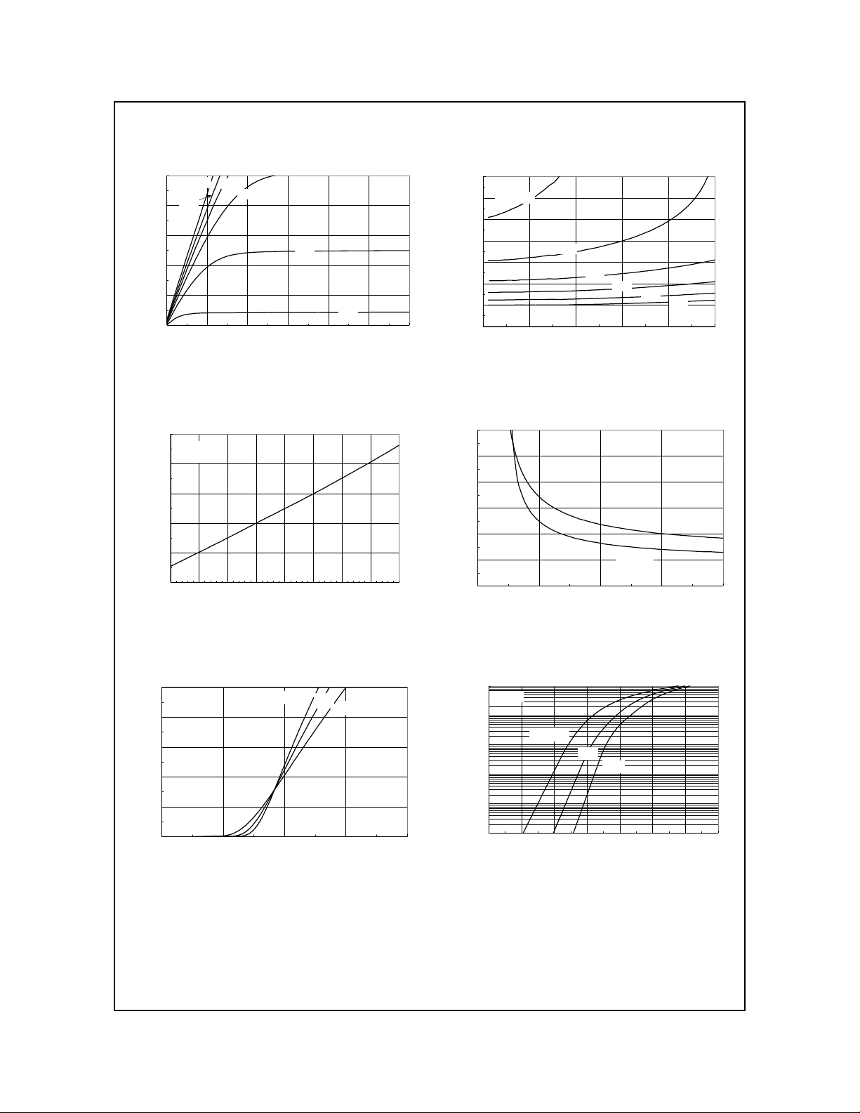
T ypical Characteristics
FDN335N
10
VGS = 4.5V
8
6
4
, DRAIN CURRENT (A)
D
I
2
0
00.511.522.53
3.5V
3.0V
2.5V
2.0V
, DRAIN TO SOURCE VOLTAGE (V)
V
DS
1.5V
Figure 1. On-Region Characteristics.
1.6
ID = 1.7A
V
= 4.5V
GS
1.4
1.2
, NORMALIZED
1
DS(ON)
R
0.8
DRAIN-SOURCE ON-RESISTANCE
0.6
-50 -25 0 25 50 75 100 125 150
, JUNCTION TEMPERATURE (oC)
T
J
2.2
VGS = 2.0V
2
1.8
1.6
1.4
, NORMALIZED
DS(ON)
1.2
R
1
DRAIN-SOURCE ON-RESISTANCE
0.8
0246810
2.5V
3.0V
3.5V
, DRAIN CURRENT (A)
I
D
4.0V
4.5V
Figure 2. On-Resistance Variation
with Drain Current and Gate V oltage.
0.24
0.2
0.16
0.12
0.08
, ON-RESISTANCE (OHM)
DS(ON)
0.04
R
0
12345
, GATE TO SOURCE VOLTAGE (V)
V
GS
TA = 125oC
TA = 25oC
ID = 0.85A
Figure 3. On-Resistance Variation
with Temperature.
10
VDS = 5V
8
6
4
, DRAIN CURRENT (A)
D
I
2
0
01234
V
GS
TA = -55oC
, GATE TO SOURCE VOLTAGE (V)
25oC
125oC
Figure 4. On-Resistance Variation
with Gate-to-Source V oltage.
10
VGS = 0V
1
0.1
0.01
0.001
, REVERSE DRAIN CURRENT (A)
S
I
0.0001
0 0.2 0.4 0.6 0.8 1 1.2 1.4
TA = 125oC
25oC
-55oC
, BODY DIODE FORWARD VOLTAGE (V)
V
SD
Figure 5. Transfer Characteristics. Figure 6. Body Diode Forward Voltage
Variation with Source Current
and Temperature.
FDN335N Rev. C
 Loading...