

Fairchild Semiconductor FDN304P Datasheet
FDN304P
P-Channel 1.8V Specified PowerTrench
MOSFET
FDN304P
June 2000
PRELIMINARY
General Description
This P-Channel 1.8V specified MOSFET uses
Fairchild’s advanced low voltage PowerTrench process.
It has been optimized for battery power management
applications.
Applications
• Battery management
• Load switch
• Battery protection
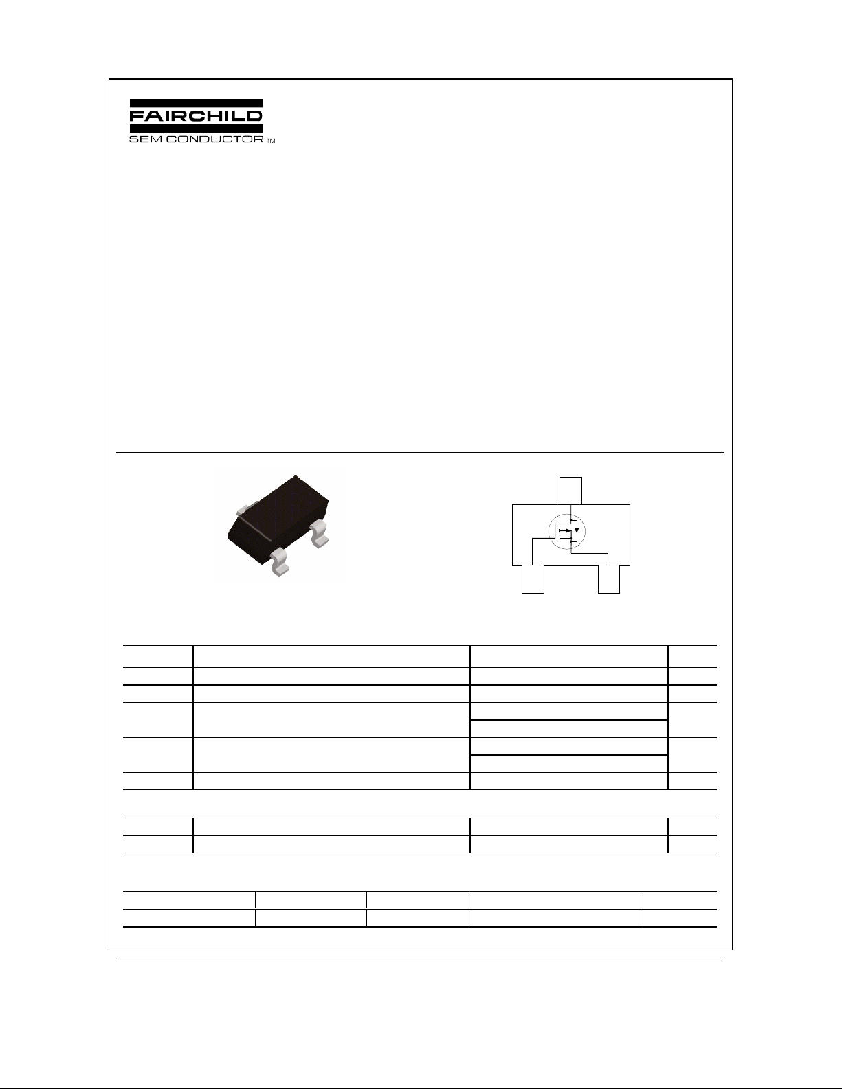
D
Features
• –2.4 A, –20 V. R
R
R
• Fast switching speed
• High performance trench technology for extremely
low R
DS(ON)
• SuperSOTTM -3 provides low R
power handling capability than SOT23 in the same
footprint
= 0.052 Ω @ VGS = –4.5 V
DS(ON)
= 0.070 Ω @ VGS = –2.5 V
DS(ON)
= 0.100 Ω @ VGS = –1.8 V
DS(ON)
and 30% higher
DS(ON)
D
S
G
SuperSOT -3
TM
Absolute Maximum Ratings T
G
=25oC unless otherwise noted
A
Symbol Parameter Ratings Units
V
DSS
V
GSS
I
D
D
TJ, T
STG
Drain-Source Voltage –20 V
Gate-Source Voltage
Drain Current – Continuous (Note 1a)
– Pulsed
Maximum Power Dissipation (Note 1a) 0.5P
(Note 1b)
Operating and Storage Junction Temperature Range -55 to +150
±8
–2.4
–10
0.46
S
V
A
W
°C
Thermal Characteristics
R
θJA
R
θJC
Thermal Resistance, Junction-to-Ambient (Note 1a) 250
Thermal Resistance, Junction-to-Case (Note 1) 75
Package Marking and Ordering Information
Device Marking Device Reel Size Tape width Quantity
.304 FDN304P 7’’ 8mm 3000 units
2000 Fairchild Semiconductor Corporati on
°C/W
°C/W
FDN304P Rev B(W)
Electrical Characteristics T
= 25°C unless otherwise noted
A
Symbol Parameter Test Conditions Min Typ Max Units
Off Characteristics
BV
DSS
∆BVDSS
===∆T
I
DSS
I
GSSF
I
GSSR
Drain–Source Breakdown Voltage
Breakdown Voltage Temperature
Coefficient
J
V
= 0 V, ID = –250 µA
GS
I
= –250 µA,Referenced to 25°C
D
–20 V
–13
Zero Gate Voltage Drain Current VDS = –16 V, VGS = 0 V –1
Gate–Body Leakage, Forward VGS = 8 V, VDS = 0 V 100 nA
Gate–Body Leakage, Reverse VGS = –8 V VDS = 0 V –100 nA
mV/°C
On Characteristics (Note 2)
V
GS(th)
∆VGS(th)
===∆T
R
DS(on)
I
D(on)
g
FS
Gate Threshold Voltage
Gate Threshold Voltage
Temperature Coefficient
J
Static Drain–Source
On–Resistance
V
= VGS, ID = –250 µA
DS
I
= –250 µA,Referenced to 25°C
D
VGS = –4.5 V, ID = –2.4 A
= –2.5 V, ID = –2.0 A
V
GS
= –1.8V, ID = –1.8 A
V
GS
–0.4 –0.8 –1.5 V
3
0.036
0.047
0.065
On–State Drain Current VGS = –4.5 V, VDS = –5 V –10 A
Forward Transconductance VDS = –5 V, ID = –1.25 A 12 S
mV/°C
0.052
0.070
0.100
Dynamic Characteristics
C
iss
C
oss
C
rss
Input Capacitance 1312 pF
Output Capacitance 240 pF
Reverse Transfer Capacitance
= –10 V, V
V
DS
f = 1.0 MHz
GS
= 0 V,
106 pF
Switching Characteristics (Note 2)
t
t
t
t
Q
Q
Q
d(on)
r
d(off)
f
g
gs
gd
Turn–On Delay Time 15 27 ns
Turn–On Rise Time 15 27 ns
= –10 V, ID = –1 A,
V
DD
= –4.5 V, R
V
GS
GEN
= 6 Ω
Turn–Off Delay Time 40 64 ns
Turn–Off Fall Time
Total Gate Charge 12 20 nC
Gate–Source Charge 2 nC
V
= –10 V, ID = –2.4 A,
DS
= –4.5 V
V
GS
Gate–Drain Charge
25 40 ns
2nC
Drain–Source Diode Characteristics and Maximum Ratings
I
S
V
SD
Notes:
1. R
θJA
the drain pins. R
Maximum Continuous Drain–Source Diode Forward Current –0.42 A
Drain–Source Diode Forward
VGS = 0 V, IS = –0.42 (Note 2) –0.6 –1.2 V
Voltage
is the sum of the junction-to-case and case-to-ambient thermal resistance where the case thermal reference is defined as the solder mounting surface of
is guaranteed by design while R
θJC
is determined by the user's board design.
θCA
µA
Ω
a) 250°C/W when mounted on a
2
0.02 in
pad of 2 oz. copper.
Scale 1 : 1 on letter size paper
2. Pulse Test: Pulse Width ≤=300 µs, Duty Cycle ≤=2.0%
b) 270°C/W when mounted on a
minimum pad.
FDN304P Rev B(W)
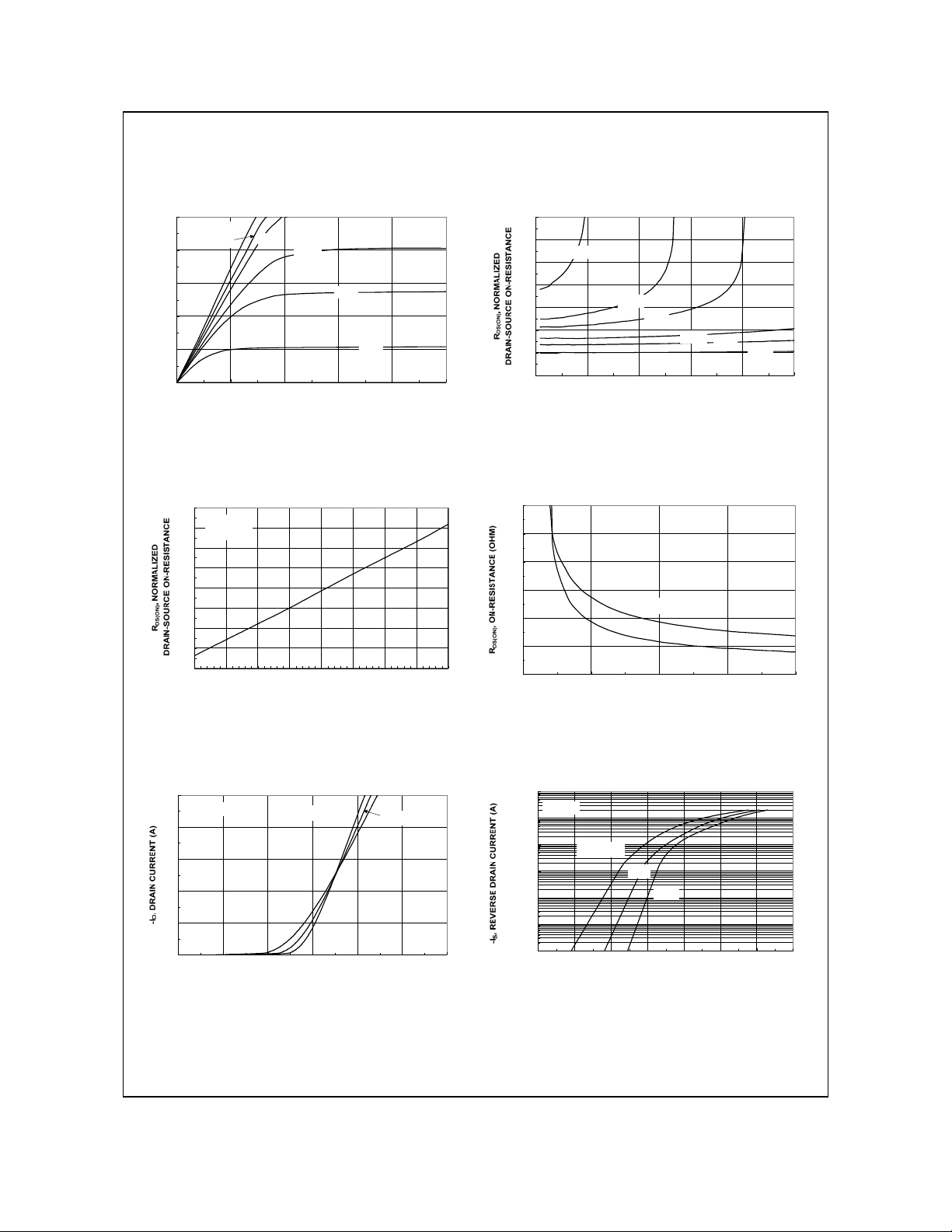
Typical Characteristics
)
FDN304P
15
VGS = -4.5V
12
9
6
, DRAIN CURRENT (A
D
-I
3
0
-3.0V
00.511.522.5
-2.5V
-2.0V
-1.8V
-V
, DRAIN-SOURCE VOLTAGE (V)
DS
-1.5V
4
3.5
VGS = -1.5V
3
2.5
2
1.5
1
0.5
03691215
-1.8V
-2.0V
-2.5V
-I
, DRAIN CURRENT (A)
D
Figure 1. On-Region Characteristics. Figure 2. On-Resistance Variation with
Drain Current and Gate Voltage.
1.5
ID = -2.4A
1.4
V
= -4.5V
GS
1.3
1.2
1.1
1
0.9
0.8
0.7
-50 -25 0 25 50 75 100 125 150
, JUNCTION TEMPERATUR E (oC)
T
J
0.14
0.12
0.1
0.08
0.06
TA = 25oC
0.04
0.02
12345
-V
TA = 125oC
, GATE TO SOURCE VOLTAGE (V)
GS
-3.0V
-4.5V
ID = -1.2 A
Figure 3. On-Resistance Variation with
Temperature.
15
VDS = - 5V
12
9
6
3
0
0 0.5 1 1.5 2 2.5 3
-V
, GATE TO SOURCE VOLTAGE (V)
GS
TA =
25oC
-55oC
Figure 4. On-Resistance Variation with
Gate-to-Source Voltage.
100
VGS = 0V
10
1
0.1
0.01
0.001
0.0001
TA = 125oC
25oC
-55oC
0 0.2 0.4 0.6 0.8 1 1.2 1.4
, BODY DIODE FOR WARD VOLTAG E (V)
-V
SD
Figure 5. Transfer Characteristics. Figure 6. Body Diode Forward Voltage Variation
with Source Current and Temperature.
FDN304P Rev B(W)
 Loading...