

Fairchild Semiconductor DM74S00N, DM74S00M, DM74S00CW Datasheet
© 2000 Fairchild Semiconductor Corporation DS006489 www.fairchildsemi.com
August 1986
Revised May 2000
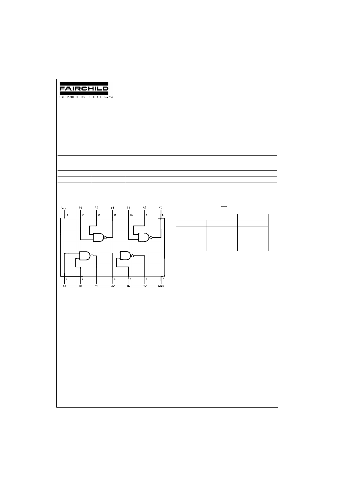
DM74S00 Quad 2-Input NAND Gate
DM74S00
Quad 2-Input NAND Gate
General Description
This device contains four in dep en den t ga tes ea ch of w hich
performs the logic NAND function.
Ordering Code:
Devices also availab le in Tape and Reel. Specify by appending th e s uffix let t er “X” to the ordering code.
Connection Diagram Function Table
Y = AB
H = HIGH Logic Level
L = LOW Logic Level
Order Number Package Number Package Description
DM74S00M M14A 14-Lead Small Outline Integrated Circuit (SOIC), JEDEC MS-120, 0.150 Narrow
DM74S00N N14A 14-Lead Plastic Dual-In-Line Package (PDIP), JEDEC MS-001, 0.300 Wide
Inputs Output
ABY
LLH
LHH
HLH
HHL
www.fairchildsemi.com 2
DM74S00
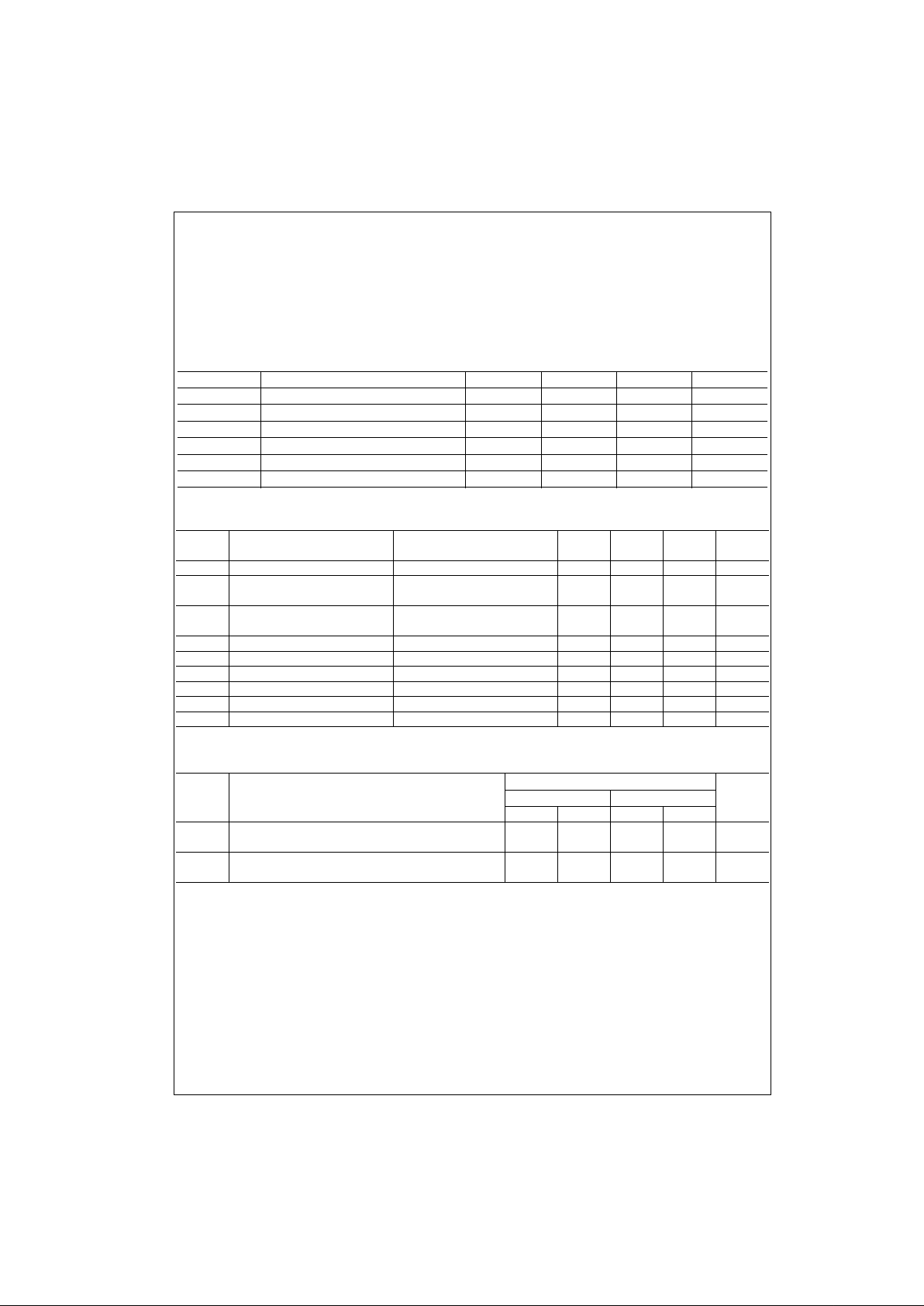
Absolute Maximum Ratings(Note 1)
Note 1: The “Absolute Maximum Ratings” are those values beyond which
the safety of the dev ice cannot be guaranteed. T he device sh ould not be
operated at these limit s. The parametric values defin ed in the Electrical
Characteristics tables are not guaranteed at the absolute maximum ratings.
The “Recomme nded O peratin g Cond itions ” table will defin e the condition s
for actual device operation.
Recommended Operating Conditions
Electrical Characteristics
over recommended operating free air temperature range (unless otherwise noted)
Switching Characteristics
at V
CC
= 5V and T
A
= 25°C (See Section 1 for Test Waveforms and Output Load)
Note 2: All typicals are at VCC = 5V, TA = 25°C.
Note 3: Not more than one output should be shorted at a t im e and the duration should not exceed one second.
Supply Voltage 7V
Input Voltage 5.5V
Operating Free Air Temperature Range 0°C to +70°C
Storage Temperature Range −65°C to +150°C
Symbol Parameter Min Nom Max Units
V
CC
Supply Voltage 4.75 5 5.25 V
V
IH
HIGH Level Input Voltage 2 V
V
IL
LOW Level Input Voltage 0.8 V
I
OH
HIGH Level Output Current −1mA
I
OL
LOW Level Output Current 20 mA
T
A
Free Air Operating Temperature 0 70 °C
Symbol Parameter Conditions Min
Typ
Max Units
(Note 2)
V
I
Input Clamp Voltage VCC = Min, II = −18 mA −1.2 V
V
OH
HIGH Level VCC = Min, IOH = Max 2.7 3.4
V
Output Voltage VIL = Max
V
OL
LOW Level VCC = Min, IOL = Max
0.5 V
Output Voltage VIH = Min
I
I
Input Current @ Max Input Voltage VCC = Max, VI = 5.5V 1 mA
I
IH
HIGH Level Input Current VCC = Max, VI = 2.7V 50 µA
I
IL
LOW Level Input Current VCC = Max, VI = 0.5V −2mA
I
OS
Short Circuit Output Current VCC = Max (Note 3) −40 −100 mA
I
CCH
Supply Current with Outputs HIGH VCC = Max 10 16 mA
I
CCL
Supply Current with Outputs LOW VCC = Max 20 36 mA
R
L
= 280Ω
Symbol Parameter C
L
= 15 pF CL = 50 pF Units
MinMaxMinMax
t
PLH
Propagation Delay Time
24.52 7ns
LOW-to-HIGH Level Output
t
PHL
Propagation Delay Time
2528ns
HIGH-to-LOW Level Output
 Loading...