

Fairchild Semiconductor DM74LS279N, DM74LS279MX, DM74LS279M Datasheet
© 2000 Fairchild Semiconductor Corporation DS006420 www.fairchildsemi.com
August 1986
Revised March 2000
DM74LS279 Quad S-R Latch
DM74LS279
Quad S
-R Latch
General Description
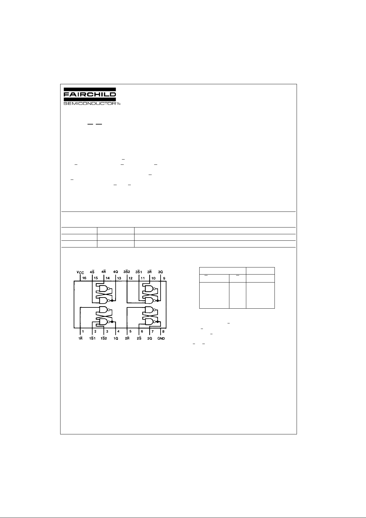
The DM74LS279 consist s of four individual and indepe ndent Set-Reset Latches with active low inputs. Two of the
four latches have an add itiona l S
input ANDed with the pri-
mary S
input. A LOW on any S input while the R input is
HIGH will be stored in the latch and appear on the corresponding Q output as a HIGH. A LOW on the R
input while
the S
input is HIGH will clear the Q output to a LOW. Simul-
taneous transition of the R
and S inputs from LOW-toHIGH will cause the Q output to be indetermina te. Both
inputs are voltage leve l triggered and are no t affected by
transition time of the input data.
Ordering Code:
Devices also availab le in Tape and Reel. Specify by appending th e s uffix let t er “X” to the ordering code.
Connection Diagram Function Table
H = HIGH Level
L = LOW Level
Q0 = The Level of Q before the indica t ed input conditions were established.
Note 1: For latches with double S
inputs:
H = both S
inputs HIGH
L = one or both S
inputs LOW
Note 2: This output level is pse udo st able; that is, it may not per sist when
the S
and R inputs return to their inactive (HIGH) level.
Order Number Package Number Package Description
DM74LS279M M16A 16-Lead Small Outline Integrated Circuit (SOIC), JEDEC MS-012, 0.150 Narrow
DM74LS279N N16E 16-Lead Plastic Dual-In-Line Package (PDIP), JEDEC MS-001, 0.300 Wide
Inputs Output
S
(Note 1) R Q
L L H (Note 2)
LHH
HLL
HHQ
0
www.fairchildsemi.com 2
DM74LS279
Absolute Maximum Ratings(Note 3)
Note 3: The “Absolute Maximum Ratin gs” are those v alues beyon d which
the safety of the dev ice cannot be guaranteed. T he device sh ould not be
operated at these limits. The parametric values defined in the Electrical
Characteristics tables are not guaranteed at the absolute maximum ratings.
The “Recommend ed O peratin g Cond itions” t able w ill defin e the co ndition s
for actual device operation.
Recommended Operating Conditions
Electrical Characteristics
over recommended operating free air temperature range (unless otherwise noted)
Note 4: All typicals are at VCC = 5V, TA = 25°C.
Note 5: Not more than one output should be shorted at a time, and the duration should not exceed one second.
Note 6: I
CC
is measured with all R in puts grounded, all S input s at 4. 5V and all outputs OPEN.
Switching Characteristics
at VCC = 5V and TA = 25°C
Supply Voltage 7V
Input Voltage 7V
Operating Free Air Temperature Range 0°C to +70°C
Storage Temperature Range −65°C to +150°C
Symbol Parameter Min Nom Max Units
V
CC
Supply Voltage 4.75 5 5.25 V
V
IH
HIGH Level Input Voltage 2 V
V
IL
LOW Level Input Voltage 0.8 V
I
OH
HIGH Level Output Current −0.4 mA
I
OL
LOW Level Output Current 8 mA
T
A
Free Air Operating Temperature 0 70 °C
Symbol Parameter Conditions Min
Typ
Max Units
(Note 4)
V
I
Input Clamp Voltage VCC = Min, II = −18 mA −1.5 V
V
OH
HIGH Level VCC = Min, IOH = Max
2.7 3.5 V
Output Voltage VIL = Max, VIH = Min
V
OL
LOW Level VCC = Min, IOL = Max
0.35 0.5
Output Voltage VIL = Max, VIH = Min V
IOL = 4 mA, VCC = Min 0.25 0.4
I
I
Input Current @ Max Input Voltage VCC = Max, VI = 7V 0.1 mA
I
IH
HIGH Level Input Current VCC = Max, VI = 2.7V 20 µA
I
IL
LOW Level Input Current VCC = Max, VI = 0.4V −0.4 mA
I
OS
Short Circuit Output Current VCC = Max (Note 5) −20 −100 mA
I
CC
Supply Current VCC = Max (Note 6) 3.8 7 mA
From (Input)
RL = 2 kΩ
Symbol Parameter
To (Output)
CL = 15 pF CL = 50 pF Units
Min Max Min Max
t
PLH
Propagation Delay Time
S to Q 22 25 ns
LOW-to-HIGH Level Output
t
PHL
Propagation Delay Time
S to Q 15 23 ns
HIGH-to-LOW Level Output
t
PHL
Propagation Delay Time
R to Q 27 33 ns
HIGH-to-LOW Level Output
 Loading...