

Fairchild Semiconductor DM74LS132M, DM74LS132CW, DM74LS132SJ, DM74LS132N, DM74LS132MX Datasheet
© 2000 Fairchild Semiconductor Corporation DS006389 www.fairchildsemi.com
August 1986
Revised March 2000
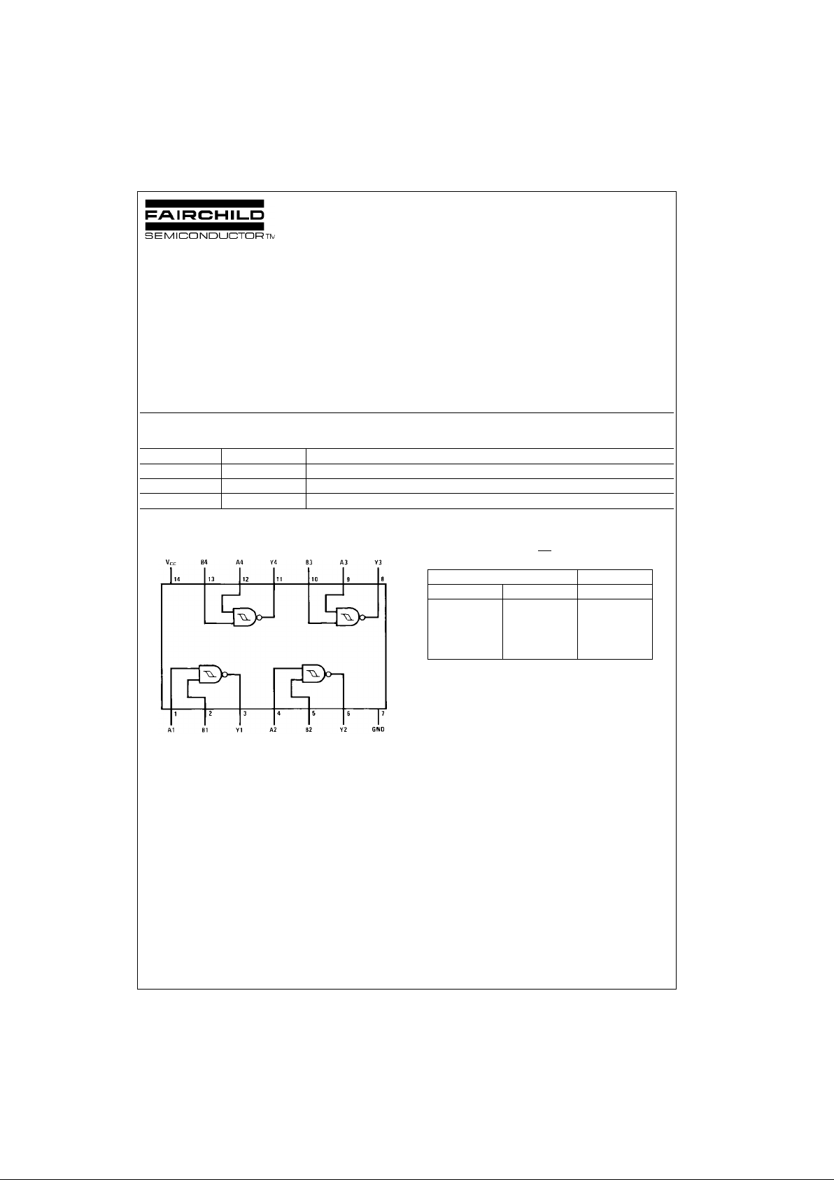
DM74LS132 Quad 2-Input NAND Gate with Schmitt Trigger Input
DM74LS132
Quad 2-Input NAND Gate with Schmitt Trigger Input
General Description
This device contains four independent gates each of which
performs the logic NA ND fu nctio n. Each input has hyster esis which increases the noise immunity and transforms a
slowly changing input signal to a fast changing, jitter free
output.
Ordering Code:
Devices also availab le in Tape and Reel. Specify by appending th e s uffix let t er “X” to the ordering code.
Connection Diagram Function Table
Y = AB
H = HIGH Logic Level
L = LOW Logic Level
Order Number Package Number Package Description
DM74LS132M M14A 14-Lead Small Outline Integrated Circuit (SOIC), JEDEC MS-120, 0.150 Narrow
DM74LS132SJ M14D 14-Lead Small Outline Package (SOP), EIA J TYPE II, 5.3mm Wide
DM74LS132N N14A 14-Lead Plastic Dual-In-Line Package (PDIP), JEDEC MS-001, 0.300 Wide
Inputs Output
ABY
LLH
LHH
HLH
HHL
www.fairchildsemi.com 2
DM74LS132
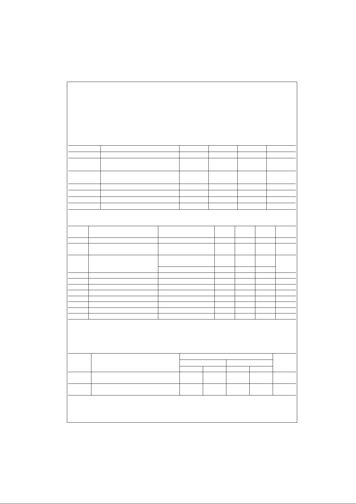
Absolute Maximum Ratings(Note 1)
Note 1: The “Absolute Maximum Ratin gs” are those v alues beyon d which
the safety of the dev ice cannot be guaranteed. T he device sh ould not be
operated at these limits. The paramet ric values defined in the “Electrical
Characteristics” ta ble are not guaranteed at the absolute maximum ratings.
The “Recommend ed O peratin g Cond itions” t able w ill defin e the co ndition s
for actual device operation.
Recommended Operating Conditions
Electrical Characteristics
over recommended operating free air temperature range (unless otherwise noted)
Note 2: VCC = 5V
Note 3: All typicals are at V
CC
= 5V, TA = 25°C.
Note 4: Not more than one output should be shorted at a time, and the duration should not exceed one second.
Switching Characteristics
at VCC 5V and TA = 25°C
Supply Voltage 7V
Input Voltage 7V
Operating Free Air Temperature Range 0°C to +70°C
Storage Temperature Range −65°C to +150°C
Symbol Parameter Min Nom Max Units
V
CC
Supply Voltage 4.75 5 5.25 V
V
T+
Positive-Going Input
1.4 1.6 1.9 V
Threshold Voltage (Note 2)
V
T−
Negative-Going Input
0.5 0.8 1 V
Threshold Voltage (Note 2)
HYS Input Hysteresis (Note 2) 0.4 0.8 V
I
OH
HIGH Level Output Current −0.4 mA
I
OL
LOW Level Output Current 8 mA
T
A
Free Air Operating Temperature 0 70 °C
Symbol Parameter Conditions Min
Typ
Max Units
(Note 3)
V
I
Input Clamp Voltage VCC = Min, II = −18 mA −1.5 V
V
OH
HIGH Level VCC = Min, IOH = Max,
2.7 3.4 V
Output Voltage VI = VT− Min
V
OL
LOW Level VCC = Min, IOL = Max,
0.35 0.5
Output Voltage VI = VT+ Max V
IOL = 4 mA, VCC = Min 0.25 0.4
I
T+
Input Current at Positive-Going Threshold VCC = 5V, VI = V
T+
−0.14 mA
I
T−
Input Current at Negative-Going Threshold VCC = 5V, VI = V
T−
−0.18 mA
I
I
Input Current @ Max Input Voltage VCC = Max, VI = 7V 0.1 mA
I
IH
HIGH Level Input Current VCC = Max, VI = 2.7V 20 µA
I
IL
LOW Level Input Current VCC = Max, VI = 0.4V −0.4 mA
I
OS
Short Circuit Output Current VCC = Max (Note 4) −20 −100 mA
I
CCH
Supply Current with Outputs HIGH VCC = Max 5.9 11 mA
I
CCL
Supply Current with Outputs LOW VCC = Max 8.2 14 mA
RL = 2 kΩ
Symbol Parameter
CL = 15 pF CL = 50 pF
Units
Min Max Min Max
t
PLH
Propagation Delay Time
5 22 8 25 ns
LOW-to-HIGH Level Output
t
PHL
Propagation Delay Time
5221033ns
HIGH-to-LOW Level Output
 Loading...