

Fairchild Semiconductor DM74AS158N, DM74AS158MX, DM74AS158M Datasheet
© 2000 Fairchild Semiconductor Corporation DS006290 www.fairchildsemi.com
April 1984
Revised March 2000
DM74AS157 • DM74AS158 Quad 1 of 2 Line Data Selector/Multiplexer
DM74AS157 • DM74AS158
Quad 1 of 2 Line Data Selector/Multiplexer
General Description
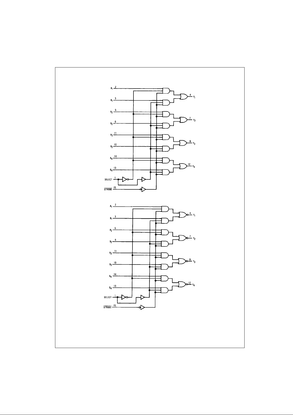
These data selectors/multiplexers contain inverters and
drivers to supply full on-chip da ta selection to the fo ur output gates. A separate STROBE
input is provided. A 4-bit
word is selected from on e of two source s and is routed to
the four outputs. The AS157 presen ts true data whereas
the AS158 presents inverted da ta to minimi ze propagat ion
delay time.
Features
■ Switching specifications at 50 pF
■ Switching specifications guaranteed over full tempera-
ture and V
CC
range
■ Advanced oxide-isolated, ion-implanted Schottky TTL
process
■ Functionally and pin for pin compatible with Schottky,
low power Schottky, and advanced low power Schottky
TTL counterpart
■ Improved AC performance over Schottky, low power
Schottky, and advanced low power Schottky counterparts
■ Expand any data input point
■ Multiplex dual data buses
■ General four functions of two variables (one variable is
common)
■ Source programmable counters
Ordering Code:
Devices also availab le in Tape and Reel. Specify by appending th e s uffix let t er “X” to the ordering code.
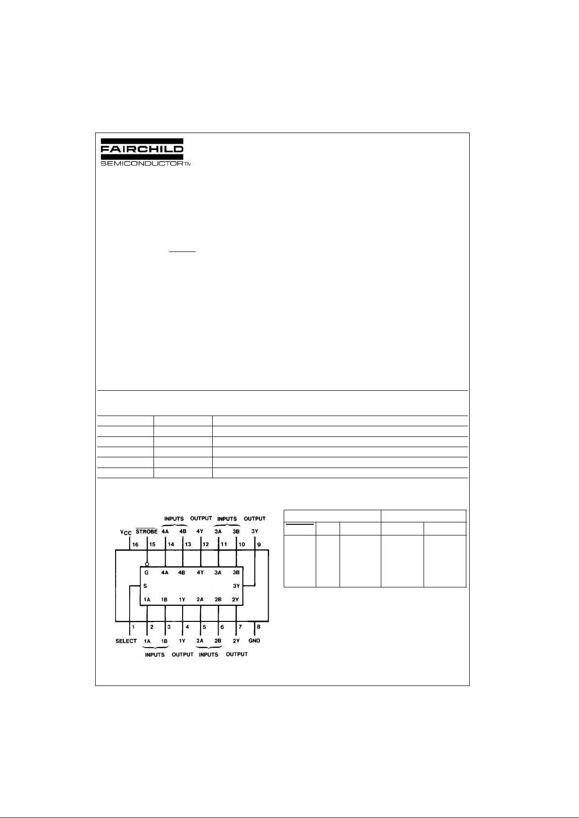
Connection Diagram Function Table
H = HIGH Level
L = LOW Level
X = Don't Care
Order Number Package Number Package Description
DM74AS157M M16A 16-Lead Small Outline Integrated Circuit (SOIC), JEDEC MS-012, 0.150 Narrow
DM74AS157SJX M16D 16-Lead Small Outline Package (SOP), EIAJ TYPE II, 5.3mm Wide
DM74AS157N N16E 16-Lead Plastic Dual-In-Line Package (PDIP), JEDEC MS-001, 0.300 Wide
DM74AS158M M16A 16-Lead Small Outline Integrated Circuit (SOIC), JEDEC MS-012, 0.150 Narrow
DM74AS158N N16E 16-Lead Plastic Dual-In-Line Package (PDIP), JEDEC MS-001, 0.300 Wide
Inputs Output Y
STROBE
Select A B DM74AS157 DM74AS158
HXXX L H
LLLX L H
LLHX H L
LHXL L H
LHXH H L
www.fairchildsemi.com 2
DM74AS157 • DM74AS158
Logic Diagrams
DM74AS157
DM74AS158
3 www.fairchildsemi.com
DM74AS157 • DM74AS158
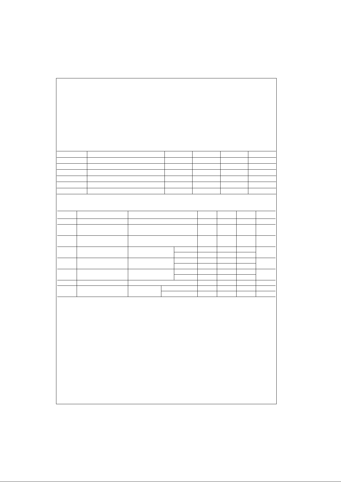
Absolute Maximum Ratings(Note 1)
Note 1: The “Absolute M aximu m R atin gs” are t hose valu es b eyo nd w hich
the safety of the device cannot be guaranteed. The device should not be
operated at these limits. The parametric values defined in the Electrical
Characteristics tables are not guaranteed at the absolute maximum ratings.
The “Recommend ed O peratin g Cond itions” t able w ill defin e the condition s
for actual device operation.
Recommended Operating Conditions
Electrical Characteristics
over recommended operating free air temperature range. All typical values are measured at VCC = 5V, TA = 25°C.
Note 2: The output con dit ions have been chosen to produce a current that closely approximates one half of the true s hort circuit current, IOS.
Supply Voltage 7V
Input Voltage 7V
Operating Free Air Temperature Range 0°C to +70°C
Storage Temperature Range −65°C to +150°C
Typical θ
JA
N Package 75.0 °C/W
Symbol Parameter Min Nom Max Units
V
CC
Supply Voltage 4.5 5 5.5 V
V
IH
HIGH Level Input Voltage 2 V
V
IL
LOW Level Input Voltage 0.8 V
I
OH
HIGH Level Output Current −2mA
I
OL
LOW Level Output Current 20 mA
T
A
Free Air Operating Temperature 0 70 °C
Symbol Parameter Conditions Min Typ Max Units
V
IK
Input Clamp Voltage VCC = 4.5V, II = −18 mA −1.2 V
V
OH
HIGH Level VCC = 4.5V to 5.5V
VCC − 2V
Output Voltage IOH = −2 mA
V
OL
LOW Level VCC = 4.5V
0.35 0.5 V
Output Voltage IOL = 20 mA
I
I
Input Current at Max VCC = 5.5V Select 0.2
mA
Input Voltage VIH = 7V All Others 0.1
I
IH
HIGH Level VCC = 5.5V Select 40
µA
Input Current VIH = 2.7V All Others 20
I
IL
LOW Level VCC = 5.5V Select −1
mA
Input Current VIL = 0.4V All Others −0.5
IO (Note 2) Output Drive Current VCC = 5.5V, VO = 2.25V −30 −112 mA
I
CC
Supply Current VCC = 5.5V DM74AS157 17.5 28 mA
DM74AS158 15.6 22.5 mA
 Loading...