Fairchild Semiconductor CQX15 Datasheet

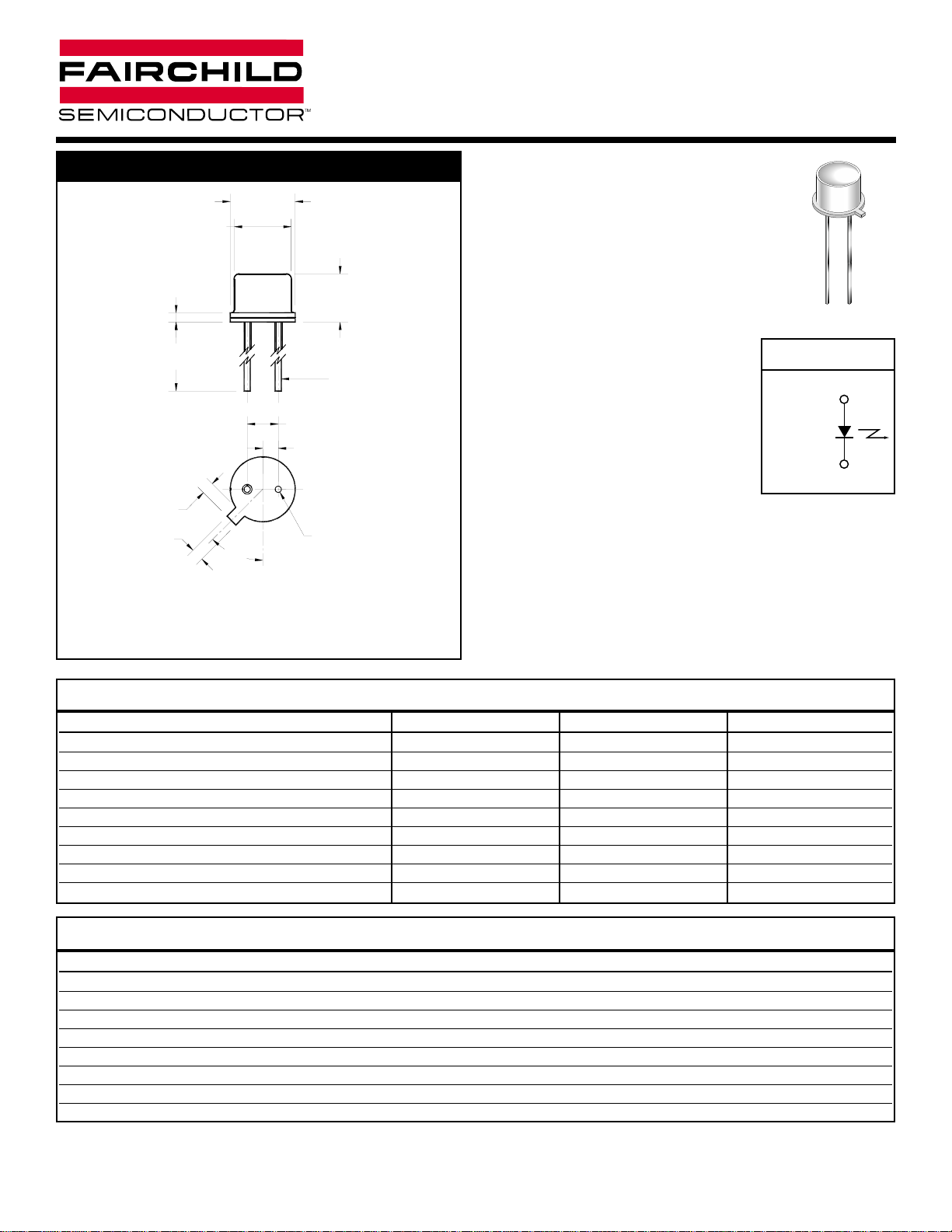
0.040 (1.02)
0.100 (2.54)
0.050 (1.27)
45°
0.040 (1.02)
13
0.030 (0.76)
NOM
0.184 (4.67)
0.209 (5.31)
1.00 (25.4)
MIN
ANODE
(CASE)
Ø0.020 (0.51) 2X
0.155 (3.94)
MAX
1. Derate power dissipation linearly 1.70 mW/°C above 25°C ambient.
2. Derate power dissipation linearly 13.0 mW/°C above 25°C case.
3. RMA flux is recommended.
4. Methanol or isopropyl alcohols are recommended as cleaning
agents.
5. Soldering iron tip
1/16” (1.6mm) minimum from housing.
6. As long as leads are not under any stress or spring tension
7. Total power output, PO, is the total power radiated by the device into
a solid angle of 2 ! steradians.
PACKAGE DIMENSIONS
FEATURES
• Good optical to mechanical alignment
• Mechanically and wavelength matched
to the TO-18 series phototransistor
• Hermetically sealed package
• High irradiance level
• European “Pro Electron” registered
Parameter Symbol Rating Unit
Operating Temperature T
OPR
-65 to +125 °C
Storage Temperature T
STG
-65 to +150 °C
Soldering Temperature (Iron)
(3,4,5 and 6)
T
SOL-I
240 for 5 sec °C
Soldering Temperature (Flow)
(3,4 and 6)
T
SOL-F
260 for 10 sec °C
Continuous Forward Current I
F
100 mA
Forward Current (pw, 1µs; 200Hz) I
F
10 A
Reverse Voltage V
R
3V
Power Dissipation(TA= 25°C)
(1)
P
D
170 mW
Power Dissipation(TC= 25°C)
(2)
P
D
1.3 W
ABSOLUTE MAXIMUM RATINGS
(TA= 25°C unless otherwise specified)
NOTES:
1. Dimensions for all drawings are in inches (mm).
2. Tolerance of ± .010 (.25) on all non-nominal dimensions
unless otherwise specified.
CQX15, CQX17
GaAs INFRARED EMITTING DIODE
DESCRIPTION
The CQX15 and CQX17 series are
940nm LEDs in a wide angle, TO-46
package.
SCHEMATIC
PARAMETER TEST CONDITIONS SYMBOL MIN TYP MAX UNITS
Peak Emission Wavelength IF= 100 mA "
PE
— 940 — nm
Emission Angle at 1/2 Power # — ±40 — Deg.
Forward Voltage IF= 100 mA V
F
— — 1.7 V
Reverse Leakage Current VR= 3 V I
R
— — 10 µA
Total Power CQX15
(7)
IF= 100 mA P
O
5.4 — — mW
Total Power CQX17
(7)
IF= 100 mA P
O
1.5 — — mW
Rise Time 0-90% of output t
r
— 1.0 — µs
Fall Time 100-10% of output t
f
— 1.0 — µs
ELECTRICAL / OPTICAL CHARACTERISTICS
(TA =25°C) (All measurements made under pulse conditions)
2001 Fairchild Semiconductor Corporation
DS300285 4/26/01 1 OF 3 www.fairchildsemi.com
ANODE
(Connected
To Case)
CATHODE
3
1

www.fairchildsemi.com 2 OF 3 4/26/01 DS300285
CQX15, CQX17
GaAs INFRARED EMITTING DIODE
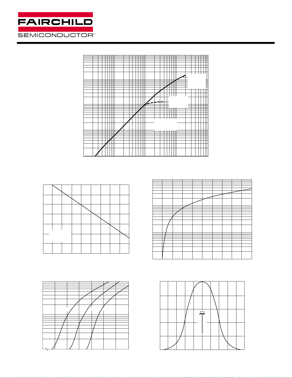
, NORMALIZED POWER OUTPUT
O
P
Figure 2. Power Output vs. Temperature
1.4
1.2
1.0
0.8
0.6
NORMALIZED TO
0.4
0.2
0
IF = 100 mA
°
C
T
= 25
A
-50
-25 0 150
, AMBIENT TEMPERATURE (°C)
T
A
, NORMALIZED POWER OUTPUT
O
P
100
50
20
10
5
2
1.0
0.5
0.2
0.1
0.05
0.02
0.01
.001 .002 .005 .01 .02 .05 0.1 0.2 0.5 1.0 2 5 10
I
, FORWARD CURRENT (A)
F
NORMALIZED TO
T
IF = 100 mA
°
C
= 25
A
CONTINUOUS
FORWARD
CURRENT
PULSED
P
= 80 µsec
W
FORWARD
CURRENT
Figure 3. Forward Voltage vs. Forward Current
10
8.0
6.0
4.0
2.0
1.0
0.8
0.6
0.4
0.2
, FORWARD CURRENT (A)
0.1
F
I
.08
.06
.04
Figure 1. Power Output vs. Input Current
755025 100 125
.02
.01
01
2
, FORWARD VOLTAGE (V)
V
F
54367109
8
Figure 4. Forward Voltage vs. Forward Current
100
80
60
40
20
10
8
6
4
, FORWARD CURRENT (mA)
F
I
2
1
TA = 100°C 25°C -55°C
.9
1.0 1.1 1.2
V
, FORWARD VOLTAGE (V)
F
100
RELATIVE OUTPUT (%)
1.51.41.3
Figure 5. Typical Radiation Pattern
80
60
40
20
0
-80 -60 -40
θ - ANGULAR DISPLACEMENT FROM OPTICAL AXIS (DEGREES)
200-20 40 60 80
 Loading...