

Fairchild Semiconductor 74LVTH32952 Datasheet
74LVTH32952
Low Voltage 32-Bit Registered Transceiver
with 3-STATE Outputs (Preli minary)
Preliminary
74LVTH32952 Low Voltage 32-Bit Registered Transceiver with 3-STATE Outputs (Preliminary)
September 2000
Revised August 2001
General Description
The LVTH32952 is a 32-bit registered transceiver. Four
8-bit back to back registers store data flowing in both directions between two bidirectional buses. Separate clock,
clock enable, and output enable sign als are provided for
each register.
The LVTH32952 data inputs includ e bushold, eliminating
the need for external pull-up resistors to hold unused
inputs.
The registered transceiver is designed for low voltage
(3.3V) V
TTL interface to a 5V environment.
The LVTH32952 is fabricated with an advanced BiCMOS
technology to achieve high speed ope ration similar to 5V
ABT while maintaining low power dissipation.
applications, but with the capability to provide a
CC
Features
■ Input and output interface capability to systems at
5V V
CC
■ Bushold data inputs eliminate the need for external
pull-up resistors to hold unused inputs
■ Live insertion/extraction per mi tt ed
■ Power Up/Down high impedance provides glitch-free
bus loading
■ Outputs source/sink
■ ESD performance:
Human-body model
Machine model
Charged-device model
■ Packaged in plastic Fine-Pitch Ball Grid Array (FBGA)
(Preliminary)
−32 mA/+64 mA
> 2000V
> 200V
Ordering Code:
Order Number Package Number Package Description
74LVTH32952GX
(Note 1)
Note 1: BGA package available in Tape and Reel only.
BGA114A
(Preliminary)
114-Ball Fine-Pitch Ball Grid Array (FBGA), JEDEC MO-205, 5.5mm Wide
[TAPE and REEL]
> 1000V
© 2001 Fairchild Semiconductor Corporation DS500411 www.fairchildsemi.com
Preliminary
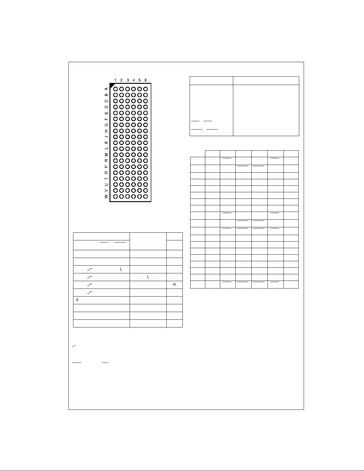
Connection Diagram
74LVTH32952
(Top Thru View)
Truth Table
(Note 2)
Inputs Internal Regis ter Output
CPAB
A
CEAnOEAB
n
XX H L NC B
XX H H NC Z
L
LL L L
L
LH L Z
H
LL H H
H
LH H Z
XL X L NC B
XH X L NC B
XL X H NC Z
XH X H NC Z
H = HIGH Voltage Level
L = LOW Voltage Level
X = Immaterial
Z = Output High Impedance
= LOW-to-HIGH Transitio n.
NC = No Change (state es t ablished by last valid C P)
B0 = State established by last valid CP
Note 2: A to B data flow shown; B to A flow contro l is the same, but uses
OEBA
, CPBAn and CEBn.
n
n
Value B
Pin Descriptions
Pin Names Description
A
0–A31
B
0–B31
CPAB
CEA
OEAB
, CPBA
n
, CEB
n
n
n
, OEBA
Data Register A Inputs
B-Register 3-STATE Outputs
Data Register B Inputs
A-Register 3-STATE Outputs
Clock Pulse Inputs
n
Clock Enable
Output Enable Inputs
n
Pin Assignments for FBGA
123456
A A
B A
C A
D A
E A
F A
G A
H A
J A15CEA2CPAB2CPBA2CEB2B
K NC CPAB3OEAB2OEBA2CPBA3NC
L A
M A
N A
0
P A
R A
T A
U A
V A
W A31CEA4OEAB4OEBA4CEB4B
0
0
CEA1CPAB1CPBA1CEB1B
0
A1OEAB1OEBA1B
2
A3GND GND B
4
A5V
6
A7GND GND B
8
A9GND GND B9B
10
12A11VCC1VCC1B11
13A14
16
18A17
20A19VCC2VCC2B19B20
22A21
24A23
26A25VCC2VCC2B25B26
28A27
29A30
GND GND B
CEA3OEAB3OEBA3CEB3B
GND GND B
GND GND B
GND GND B
GND GND B
CPAB4CPBA4B
CC1VCC1B5
B
1
B
3
B
B
7
B
14B13
17B18
21B22
23B24
27B28
30B29
0
2
4
6
8
10
12
15
16
31
www.fairchildsemi.com 2
 Loading...