Fairchild Semiconductor 74LVTH273WMX, 74LVTH273WM, 74LVTH273SJX, 74LVTH273SJ, 74LVTH273MTCX Datasheet
...
© 1999 Fairchild Semiconductor Corporation DS500100 www.fairchildsemi.com
July 1999
Revised July 1999
74LVTH273 Low Voltage Octal D-Type Flip-Flop with Clear
74LVTH273
Low Voltage Octal D-Type Flip-Flop with Clear
General Description
The LVTH273 is a high-speed, low-power positive-edgetriggered octal D-type flip-flop featuring separate D-type
inputs for each flip-flop. A buffered Clock (CP ) and Clear
(CLR
) are common to all flip-flops.
The state of each D -type input , one setup time before the
positive clock transition, is transferred to the corresponding
flip-flop’s output.
The LVTH273 data inputs include bush old, eliminati ng the
need for external pull-up resistors to hold unused inputs.
These octal flip-flops are designed for low-voltage (3.3V )
V
CC
applications, but with the capability to provide a TTL
interface to a 5V environmen t. The LVTH273 is fabricated
with an advanced BiCMOS technology to achieve high
speed operation similar to 5V ABT while maintaining low
power dissipation.
Features
■ Input and output interface capability to systems at
5V V
CC
■ Bushold on the data inputs eliminate the need for
external pull-up resistors to hold unused inputs
■ Outputs source/sink −32 mA/+64 mA
■ Functionally compatible with the 74 series 273
■ Latch-up performance exceeds 500 mA
Ordering Code:
Device also available in Tape and Reel. Specify by appending s uffix let te r “X” to the ordering code.
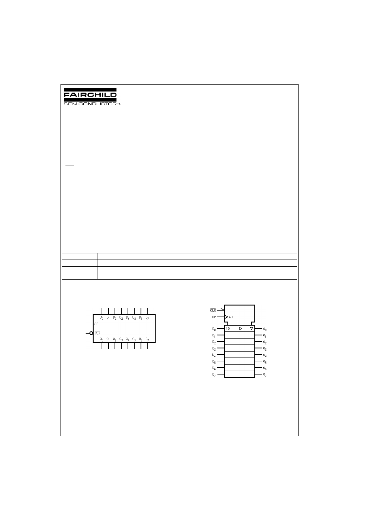
Logic Symbols
IEEE/IEC
Order Number Package Number Package Description
74LVTH273WM M20B 20-Lead Small Outline Integrated Circuit (SOIC), JEDEC MS-013, 0.300” Wide
74LVTH273SJ M20D 20-Lead Small Outline Package (SOP), EIAJ TYPE II 5.3mm Wide
74LVTH273MTC MTC20 20-Lead Thin Shrink Small Outline Package (TSSOP), JEDEC MO-153, 4.4mm Wide

www.fairchildsemi.com 2
74LVTH273
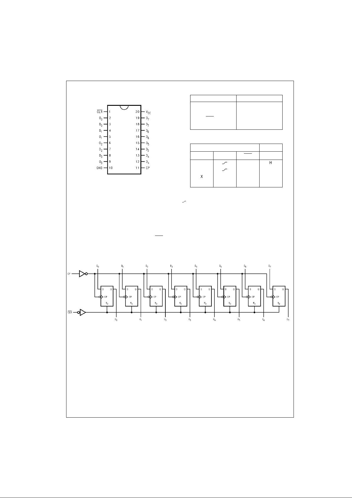
Connection Diagram Pin Descriptions
Tr uth Table
H = HIGH Voltage Level
L = LOW Voltage Level
X = Immaterial
= LOW-to-HIGH Transition
O
o
= Previous Oo before HIGH-to-LOW of CP
Functional Description
The LVTH273 consists of eight positive-edge-triggered flip-flops with individual D-type inputs. The buffered Clock and Clear
are common to all flip- fl op s. T he eig ht f l ip-flo ps w ill stor e t he stat e o f th ei r indi vid ual D -typ e inpu ts th at me et the setup and
hold time requirements on the LOW-to-HIGH Clock (CP) transition. When the Clock is either HIGH or LOW, the D-input signal has no effect at the output. When the Clear (CLR
) is LOW, all Outputs will be forced LOW.
Logic Diagram
Please note that this diagram is provided o nly f or t he understanding of lo gic operations and should not be used to estimate propagation delays.
Pin Names Description
D
0–D7
Data Inputs
CP Clock Pulse Input
CLR
Clear
O
0–O7
Outputs
Inputs Outputs
D
n
CP CLR O
n
H
HH
L
HL
XH or LH O
o
XXLL
 Loading...