

Fairchild Semiconductor 74ACTQ74SJX, 74ACTQ74SJ, 74ACTQ74SCX, 74ACTQ74SC, 74ACTQ74PC Datasheet
...
© 1999 Fairchild Semiconductor Corporation DS010920 www.fairchildsemi.com
March 1993
Revised November 1999
74ACTQ74 Quiet Series Dual D-Type
74ACTQ74
Quiet Series Dual D-Type
Positive Edge-Triggered Flip-Flop
General Description
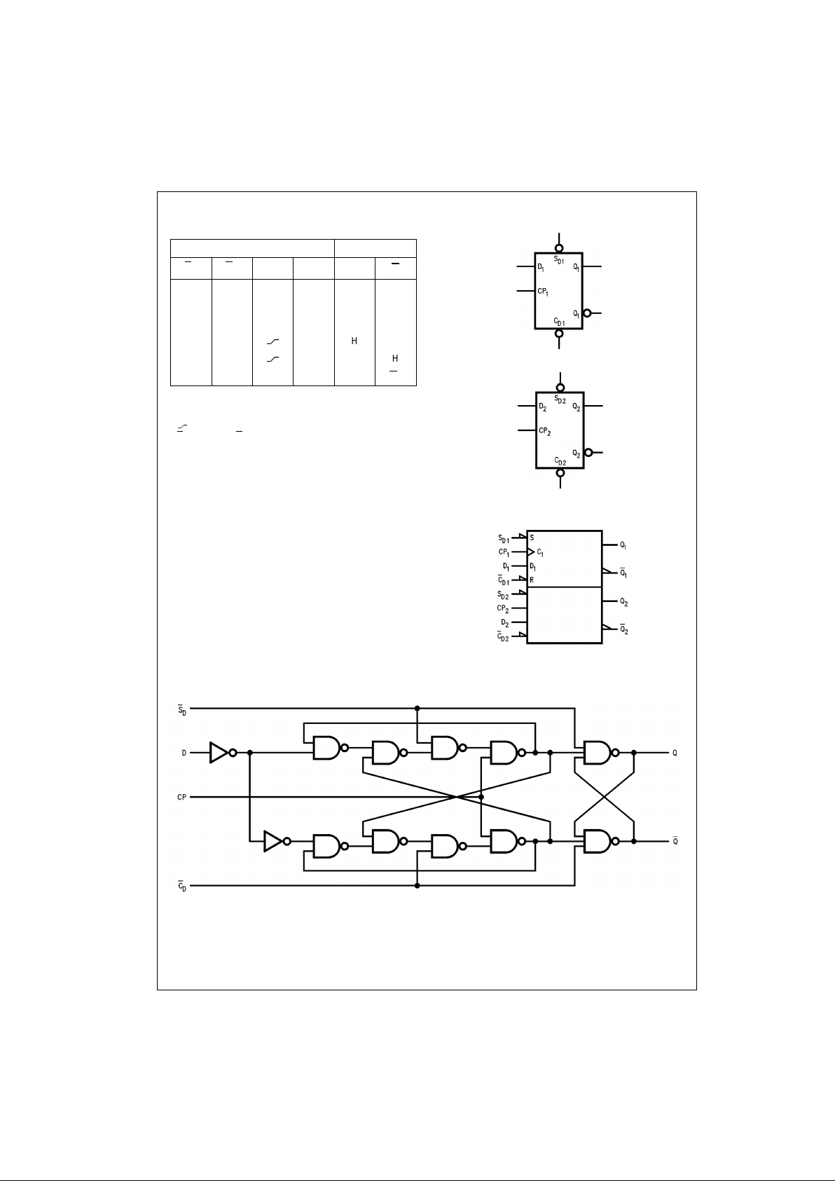
The 74ACTQ74 is a dual D-type flip-flop with Asynchronous Clear and Set inputs and complem entary (Q, Q
) outputs. Information at th e input is transferred to the outputs
on the positive edge of the clock pulse. Clock triggering
occurs at a voltage level of the clock pulse and is not
directly related t o the transition ti me of the positive-go ing
pulse. After the Clock Pulse input threshold voltage has
been passed, the Data input is lock ed out and informat ion
present will not be transferred to the out puts until the n ext
rising edge of the Clock Pulse input.
The ACTQ74 utilizes Fairchild Quiet Series technology to
guarantee quiet output switching and improved dynamic
threshold performance. FACT Quiet Series features
GTO output control and unde rshoot corre ctor in add ition
to a split ground bus for superior performance.
Asynchronous Inputs:
LOW input to S
D
(Set) sets Q to HIGH level
LOW input to C
D
(Clear) sets Q to LOW level
Clear and Set are independent of clock
Simultaneous LOW on C
D
and SD makes
both Q and Q
HIGH
Features
■ ICC reduced by 50%
■ Guaranteed simultaneous switching noise level and
dynamic threshold performan ce
■ Guarante ed pin-to-pin skew AC performance
■ Improved latch-up immunity
■ 4 kV minimum ESD immunity
■ TTL-compatible inputs
Ordering Code:
Device also available in Tape and Reel. Specify by appending suffix letter “X” to the ordering form.
Connection Diagram Pin Descriptions
FACT, FACT Quiet Series and GTO are trademarks of Fairchild Semiconductor Corporation.
Order Number Package Number Package Description
74ACTQ74SC M14A 14-Lead Small Outline Integrated Circuit (SOIC), JEDEC MS-120, 0.150 Narrow
74ACTQ74SJ M14D 14-Lead Small Outline Package (SOP), EIAJ TYPE II, 5.3mm Wide
74ACTQ74PC N14A 14-Lead Plastic Dual-In-Line Package (PDIP), JEDEC MS-001, 0.300 Wide
Pin Names Description
D
1
, D
2
Data Inputs
CP
1
, CP
2
Clock Pulse Inputs
C
D1
, C
D2
Direct Clear Inputs
S
D1
, S
D2
Direct Set Inputs
Q
1
, Q1, Q2, Q
2
Outputs
www.fairchildsemi.com 2
74ACTQ74
Truth Table
(Each Half)
H = HIGH Voltage Level
L = LOW Voltage Level
X = Immaterial
= LOW-to-HIGH Clo c k Transi ti on
Q
0(Q0
) = Previous Q(Q) before LOW-to-HIGH Transition of Clock
Logic Symbols
IEEE/IEC
Block Diagram
Please note that this diagram is provided only for the understanding of logic operations and should not be used to estimate propagation delays.
Inputs Outputs
S
D
C
D
CP D Q Q
LHXXHL
HLXXLH
LLXXHH
HH
HHL
HH
LLH
HHLXQ
0
Q
0
3 www.fairchildsemi.com
74ACTQ74
Absolute Maximum Ratings(Note 1) Recommended Operating
Conditions
Note 1: Absolute maximu m rating s are thos e values be yond wh ich dam-
age to the device may occur. The databook specifications should be met,
without exception, to ensure that the system design is reliable over its
power supply, temperature, an d output/input loading variables. Fair child
does not re c om m end operation of FACT circuits outside datab ook specifications.
DC Electrical Characteristics
Note 2: All outputs loaded; thres holds on input associate d w it h output under test.
Note 3: Maximum test duration 2.0 ms, one output loaded at a time.
Note 4: PDIP package.
Note 5: Max number of outputs defined as (n). Data inputs are driven 0V to 3V. One output @ GND.
Note 6: Max number of data input s (n ) s w it c hing. (n − 1) inputs switching 0V to 3V. Input-under-test switching:
3V to threshold (V
ILD
), 0V to threshold (V
IHD
), f = 1 MHz.
Supply Voltage (VCC) −0.5V to +7.0V
DC Input Diode Current (I
IK
)
V
I
= −0.5V −20 mA
V
I
= VCC + 0.5V +20 mA
DC Input Voltage (V
I
) −0.5V to VCC + 0.5V
DC Output Diode Current (I
OK
)
V
O
= −0.5V −20 mA
V
O
= VCC + 0.5V +20 mA
DC Output Voltage (V
O
) −0.5V to VCC + 0.5V
DC Output Source
or Sink Current (I
O
) ± 50 mA
DC V
CC
or Ground Current
per Output Pin (I
CC
or I
GND
) ± 50 mA
Storage Temperature (T
STG
) −65°C to +150°C
DC Latch-Up Source or Sink Current ± 300 mA
Junction Temperature (T
J
) PDIP 140°C
Supply Voltage (V
CC
) 4.5V to 5.5V
Input Voltage (V
I
) 0V to V
CC
Output Voltage (VO) 0V to V
CC
Operating Temperature (TA) −40°C to +85°C
Minimum Input Edge Rate ∆V/∆t
V
IN
from 0.8V to 2.0V
V
CC
@ 4.5V, 5.5V 125 mV/ns
Symbol Parameter
V
CC
TA = +25°C TA = −40°C to +85°C
Units Conditions
(V) Typ Guaranteed Limits
V
IH
Minimum HIGH Level 4.5 1.5 2.0 2.0
V
V
OUT
= 0.1V
Input Voltage 5.5 1.5 2.0 2.0 or VCC − 0.1V
V
IL
Maximum LOW Level 4.5 1.5 0.8 0.8
V
V
OUT
= 0.1V
Input Voltage 5.5 1.5 0.8 0.8 or VCC − 0.1V
V
OH
Minimum HIGH Level 4.5 4.49 4.4 4.4
VI
OUT
= −50 µA
Output Voltage 5.5 5.49 5.4 5.4
4.5 3.86 3.76
V
VIN = V
IL
or V
IH
IOH = −24 mA
IOH = −24 mA (Note 2)
5.5 4.86 4.76
V
OL
Maximum LOW Level 4.5 0.001 0.1 0.1
VI
OUT
= 50 µA
Output Voltage 5.5 0.001 0.1 0.1
4.5 0.36 0.44
V
VIN = VIL or V
IH
IOL = 24 mA
I
OL
= 24 mA (Note 2)
5.5 0.36 0.44
I
IN
Maximum Input Leakage Current 5.5 ± 0.1 ± 1.0 µAVI = VCC, GND
I
OZ
Maximum 3- STATE
5.5 ± 0.5 ± 5.0 µA
VI = VIL, V
IH
Leakage Current VO = VCC, GND
I
CCT
Maximum ICC/Input 5.5 0.6 1.5 mA VI = VCC − 2.1V
I
OLD
Minimum Dynamic 5.5 75 mA V
OLD
= 1.65V Max
I
OHD
Output Current (Note 2) 5.5 −75 mA V
OHD
= 3.85V Min
I
CC
Maximum Quiescent Supply Current 5.5 2.0 20.0 µAVIN = VCC or GND
V
OLP
Quiet Output Maximum
5.0 1.1 1.5 V
Figure 1, Figure 2
Dynamic V
OL
(Note 4)(Note 5)
V
OLV
Quiet Output Minimum
5.0 −0.6 −1.2 V
Figure 1, Figure 2
Dynamic V
OL
(Note 4)(Note 5)
V
IHD
Minimum HIGH Level Dynamic Input Voltage 5.0 1.9 2.2 V (Note 4)(Note 6)
V
ILD
Maximum LOW Level Dynamic Input Voltage 5.0 1.2 0.8 V (Note 4)(Note 6)
 Loading...