

Fairchild Semiconductor 74ACTQ533SCX, 74ACTQ533SC, 74ACTQ533PC, 74ACTQ533MTCX, 74ACTQ533MTC Datasheet
...
© 1999 Fairchild Semiconductor Corporation DS010630 www.fairchildsemi.com
January 1990
Revised November 1999
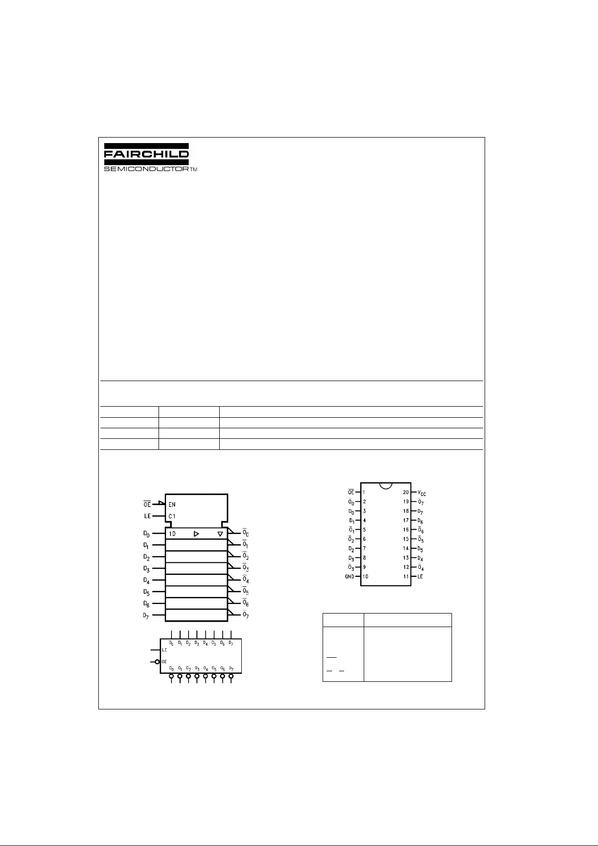
74ACTQ533 Quiet Series Octal Transparent Latch with 3-STATE Outputs
74ACTQ533
Quiet Series Octal Transparent Latch
with 3-STATE Outputs
General Description
The ACTQ533 consists of eight latch es with 3- STATE outputs for bus organized system applications. The flip-f lops
appear transparent to the data w hen Latch En able (LE) i s
HIGH. When LE is LOW, the data satisfying the input timing requirements is latched. Data appears on the bus when
the Output Enable (OE) is LOW. When OE is HIGH, the
bus output is in the high impedance state.
The ACTQ533 utilizes Fairchild Quiet Series technology
to guarantee quiet output switchin g and improve dy namic
threshold performance . FACT Quiet Series feat ure s GTO
output control and undershoot corrector in addition to a
split ground bus for superior performance.
Features
■ ICC and IOZ reduced by 5 0%
■ Guaranteed simultaneous switching noise level and
dynamic threshold performan ce
■ Guarante ed pin-to-pin skew AC performance
■ Improved latch up immunity
■ Eight latches in a single package
■ 3-STATE outputs drive bus lines or buffer memory
address registers
■ Outputs source/sink 24 mA
■ Inverted version of the ACTQ373
■ 4 kV minimum ESD immunity
Ordering Code:
Device also available in Tape and Reel. Specify by appending s uffix let te r “X” to the ordering code
Logic Symbols
IEEE/IEC
Connection Diagram
Pin Descriptions
FACT, FACT Quiet Series, and GTO are trademarks of F airchild Semiconductor Corporation.
Order Number Package Number Package Description
74ACTQ533SC M20B 20-Lead Small Outline Integrated Circuit (SOIC), JEDEC MS-013, 0.300” Wide Body
74ACTQ533MTC MTC20 20-Lead Thin Shrink Small Outline Package (TSSOP), JEDEC MO-153, 4.4mm Wide
74ACTQ533PC N20A 20-Lead Plastic Dual-In-Line Package (PDIP), JEDEC MS-001, 0.300” Wide
Pin Names Description
D
0–D7
Data Inputs
LE Lat ch Enable Input
OE
Output Enable Input
O
0–O7
3-STATE Latch Outputs
www.fairchildsemi.com 2
74ACTQ533
Truth Table
H = HIGH Voltage Level
L = LOW Voltage Level
Z = High Impedance
X = Immaterial
O
0
= Previous O0 before HIGH-to-LOW transition of Latch Enable
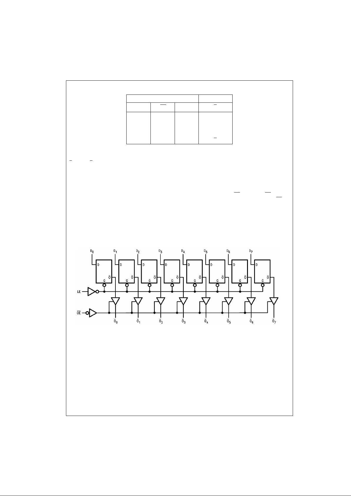
Functional Description
The ACTQ533 contains eight D-type latches with 3-STATE
standard outputs. When the Latch Enable (LE) input is
HIGH, data on the D
n
inputs enters the latches. In this con-
dition the latches are transparent, i.e., a la tch output will
change state each time its D input cha nges. When LE is
LOW, the latches store the information that was present on
the D inputs at setup time preceding the HIGH-to-LOW
transition of LE. The 3-STATE standard outputs are controlled by the Output Enab le (O E
) input. When OE is LOW,
the standard outputs are i n the 2-st ate mode. Wh en OE
is
HIGH, the standard outputs are in the high impedance
mode but this does not interfere with entering new data into
the latches.
Logic Diagram
Please note that this diagram is provided only for the understanding of logic operations and should not be used to estimate propagation delays.
Inputs Outputs
LE OE
D
n
O
n
X H X Z
H L L H
H L H L
L L X O
0
3 www.fairchildsemi.com
74ACTQ533
Absolute Maximum Ratings(Note 1) Recommended Operating
Conditions
Note 1: Absolute max imum ratings are those values beyond which damage
to the device may occu r. The databook spe cificatio ns shou ld be met, wit hout exception, to ensure that the system de sign is relia ble over its p ower
supply, temperature, and output/input loading variables. Fairchild does not
recommend operation of FACT circuits outside databook specificat ions.
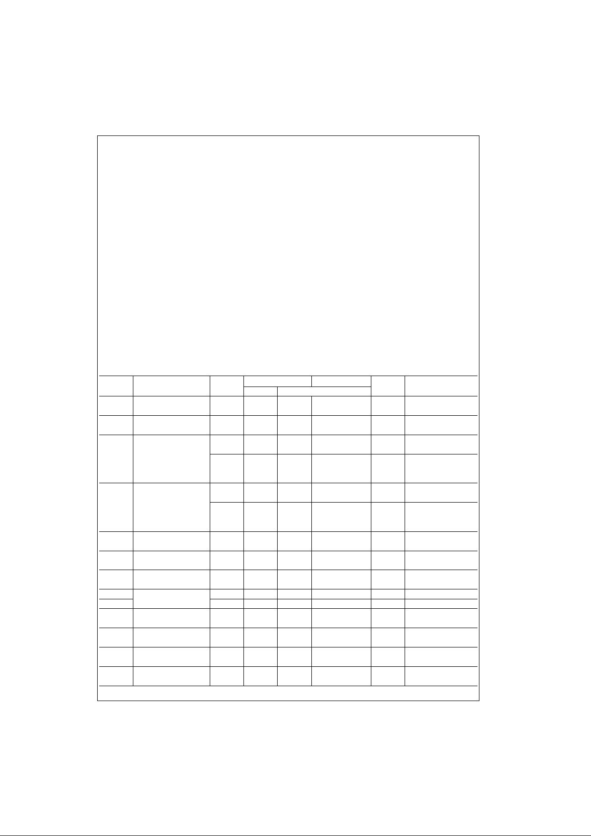
DC Electrical Characteristics
Supply Voltage (VCC) − 0.5V to + 7.0V
DC Input Diode Current (I
IK
)
V
I
= − 0.5V − 20 mA
V
I
= VCC + 0.5V + 20 mA
DC Input Voltage (V
I
) −0.5V to VCC + 0.5V
DC Output Diode Current (I
OK
)
V
O
= − 0.5V − 20 mA
V
O
= VCC + 0.5V + 20 mA
DC Output Voltage (V
O
) − 0.5V to VCC + 0.5V
DC Output Source
or Sink Current (I
O
) ± 50 mA
DC V
CC
or Ground Current
per Output Pin (I
CC
or I
GND
) ± 50 mA
Storage Temperature (T
STG
) − 65°C to + 150°C
DC Latchup Source
or Sink Current ± 300 mA
Junction Temperature (T
J
)
PDIP 140°C
Supply Voltage (V
CC
) 4.5V to 5.5V
Input Voltage (V
I
) 0V to V
CC
Output Voltage (VO) 0V to V
CC
Operating Temperature (TA) −40°C to +85°C
Minimum Input Edge Rate ∆V/∆t 125 mV/ns
V
IN
from 0.8V to 2.0V
V
CC
@ 4.5V, 5.5V
Symbol Parameter
V
CC
TA = +25°C TA = −40°C to +85°C
Units Conditions
(V) Typ Guaranteed Limits
V
IH
Minimum HIGH Level 4.5 1.5 2.0 2.0
V
V
OUT
= 0.1V
Input Voltage 5.5 1.5 2.0 2.0 or VCC − 0.1V
V
IL
Maximum LOW Level 4.5 1.5 0.8 0.8
V
V
OUT
= 0.1V
Input Voltage 5.5 1.5 0.8 0.8 or VCC − 0.1V
V
OH
Minimum HIGH Level 4.5 4.49 4.4 4.4
V I
OUT
= −50 µA
Output Voltage 5.5 5.49 5.4 5.4
V
IN
= V
IL
or V
IH
4.5 3.86 3.76 V IOH = −24 mA
5.5 4.86 4.76 IOH = −24 mA (Note 2)
V
OL
Maximum LOW Level 4.5 0.001 0.1 0.1
V I
OUT
= 50 µA
Output Voltage 5.5 0.001 0.1 0.1
VIN = V
IL
or V
IH
4.5 0.36 0.44 V IOL = 24 mA
5.5 0.36 0.44 I
OL
= 24 mA (Note 2)
I
IN
Maximum Input
5.5 ±0.1 ±1.0 µA VI = VCC, GND
Leakage Current
I
OZ
Maximum 3-STATE
5.5 ±0.25 ±2.5 µA
VI = VIL, V
IH
Leakage Current VO = VCC, GND
I
CCT
Maximum
5.5 0.6 1.5 mA VI = VCC − 2.1V
ICC/Input
I
OLD
Minimum Dynamic 5.5 75 mA V
OLD
= 1.65V Max
I
OHD
Output Current (Note 3) 5.5 −75 mA V
OHD
= 3.85V Min
I
CC
Maximum Quiescent
5.5 4.0 40.0 µA
VIN = V
CC
Supply Current or GND
V
OLP
Quiet Output
5.0 1.1 1.5 V
Figures 1, 2
Maximum Dynamic V
OL
(Note 4)(Note 5)
V
OLV
Quiet Output
5.0 −0.6 −1.2 V
Figures 1, 2
Minimum Dynamic V
OL
(Note 4)(Note 5)
V
IHD
Minimum HIGH Level
5.0 1.9 2.2 V (Note 4)(Note 6)
Dynamic Input Voltage
 Loading...