

Fairchild Semiconductor 74ACTQ18825SSCX, 74ACTQ18825SSC, 74ACTQ18825MTDX, 74ACTQ18825MTD, 74ACTQ18825CW Datasheet
© 2000 Fairchild Semiconductor Corporation DS010955 www.fairchildsemi.com
September 1991
Revised January 2000
74ACTQ18825 18-Bit Buffer/Line Driver with 3-STATE Outputs
74ACTQ18825
18-Bit Buffer/Line Driver with 3-STATE Outputs
General Description
The ACTQ18825 contains eighteen non-inverting buffers
with 3-STATE outputs designed to be employed as a memory and address driver, clock driver, or bus oriented transmitter/receiver. The device is byte controlled. Each byte
has separate 3-STATE control inputs which can be shorted
together for full 18-bit operation.
The ACTQ18825 utilizes Fairchild FACT Quiet Series
technology to guarantee quiet output switching and
improved dynamic threshold performance. FACT Quiet
Series features GTO output control and undershoot corrector for superior performance.
Features
■ Utilizes Fairchild FACT Quiet Series technology
■ Broadside pinout allows for easy board layout
■ Guaranteed simultaneous switching noise level and
dynamic threshold performance
■ Guaranteed pin-to-pin output skew
■ Separate control logic for each byte
■ Extra data width for wider address/data p aths or buses
carrying parity
■ Outputs source/sink 24 mA
■ Additional specs for Multiple Output Switching
■ Output loading specs for both 50 pF and 250 pF loads
Ordering Code:
Device also available in Tape and Reel. Specify by appending s uffix let te r “X” to the ordering code.
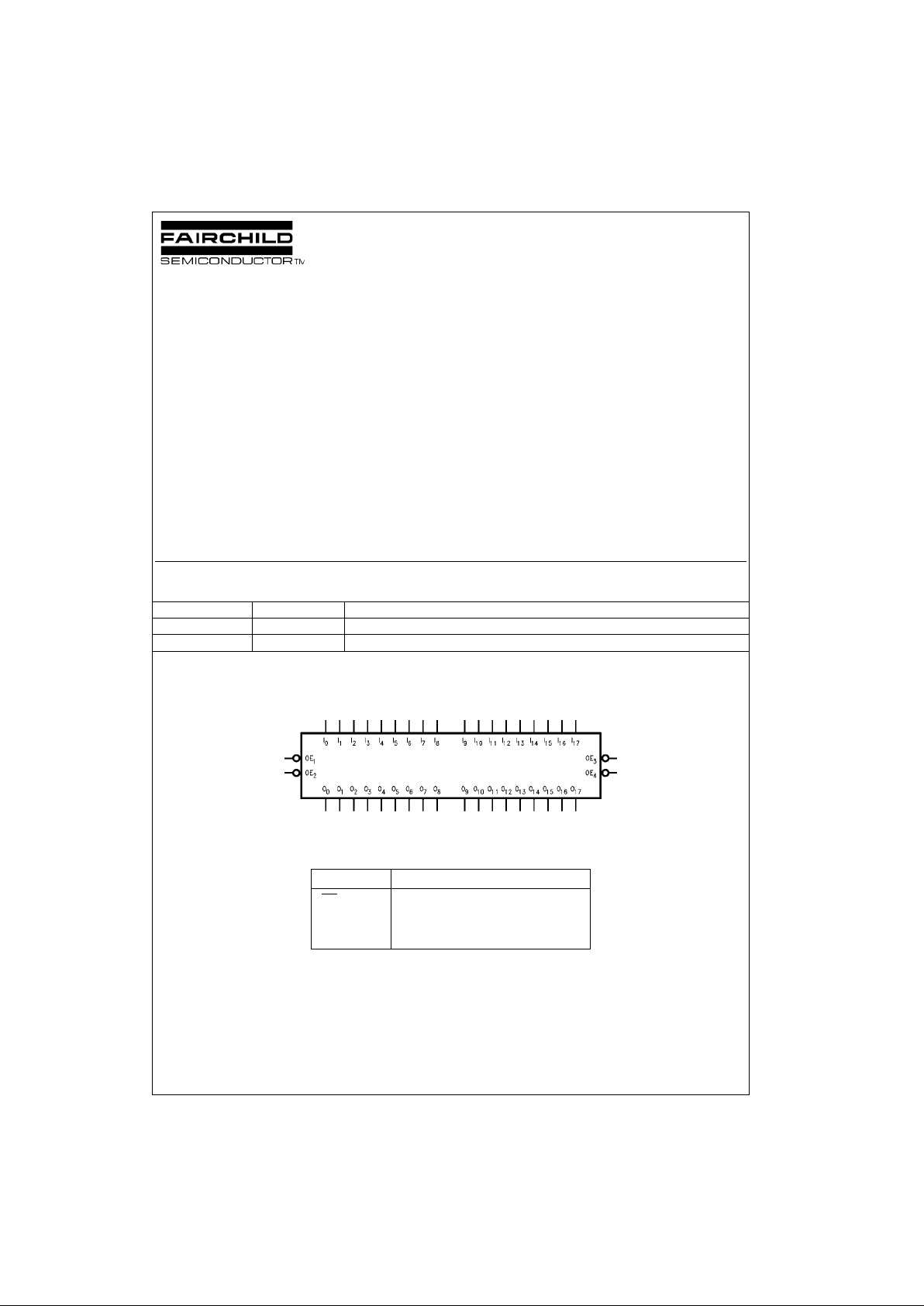
Logic Symbol
Pin Descriptions
FACT, FACT Quiet Series and GTO are trademarks of Fairc hild Semiconductor C orporation.
Order Number Package Number Package Description
74ACTQ18825SSC MS56A 56-Lead Shrink Small Outline Package (SSOP), JEDEC MO-118, 0.300” Wide
74ACTQ18825MTD MTD56 56-Lead Thin Shrink Small Outline Package (TSSOP), JEDEC MO-153, 6.1mm Wide
Pin Names Description
OE
n
Output Enable Input (Active LOW)
I
0–I17
Inputs
O
0–O17
Outputs
www.fairchildsemi.com 2
74ACTQ18825
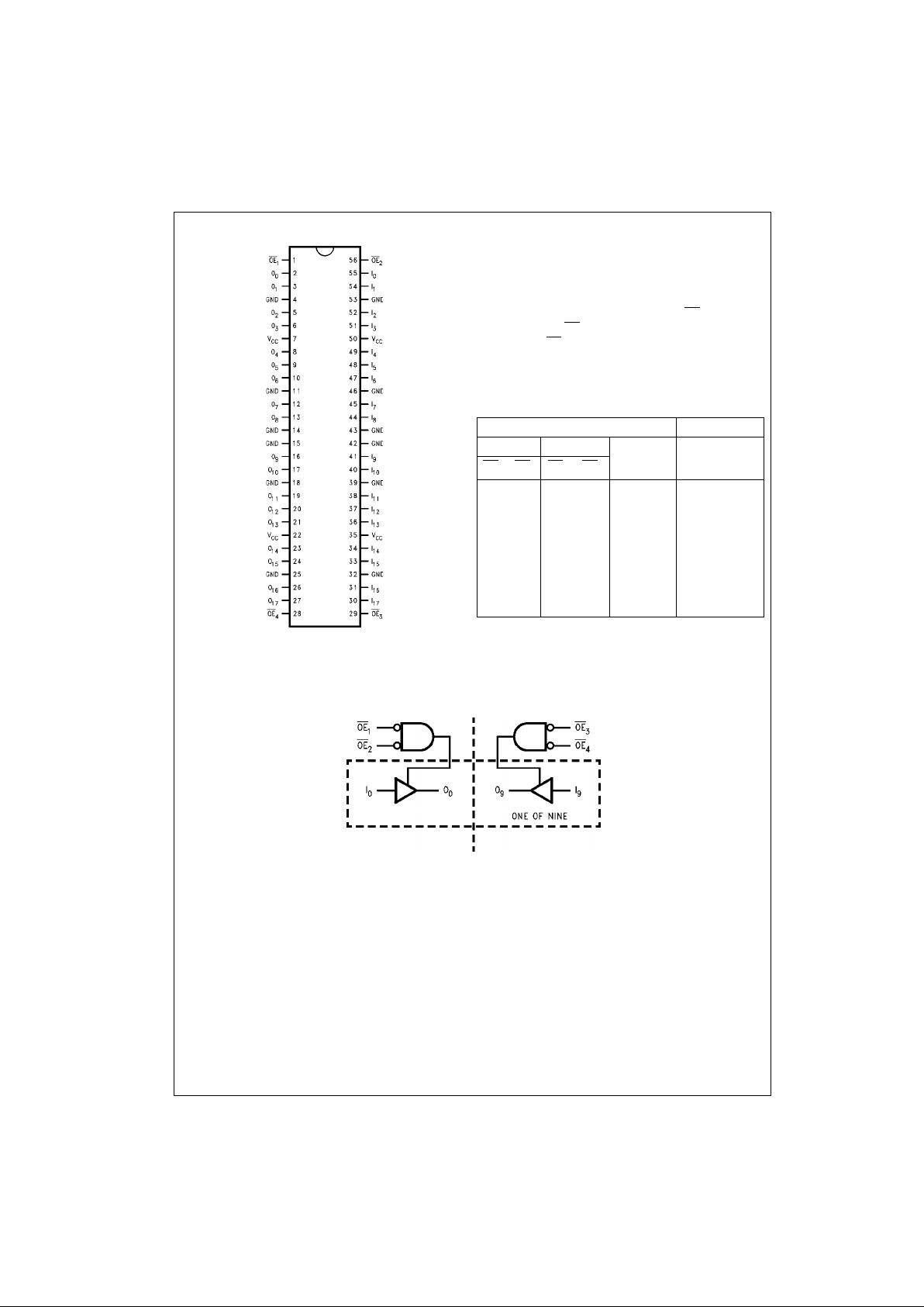
Connection Diagram Functional Description
The ACTQ18825 contains eighteen non-inverting buffers
with 3-STATE standard outputs. The device is byte controlled with each byte functioning identically, but independently of the other. The control pins may be shorted
together to obtain fu ll 18-bit operation. The 3-STATE outputs are controlle d by an Output Enable (OE
n
) input for
each byte. When OE
n
is LOW, the outputs are in 2-state
mode. When OE
n
is HIGH, the outputs are in the high
impedance mode, but this does not interfere with enteri ng
new data into the inputs.
Tr uth Table
H = HIGH Voltage Level
L = LOW Voltage Level
X = Immaterial
Z = HIGH Impedance
Logic Diagram
Inputs Outputs
Byte 1 (0:8) Byte 2 (8:17) I
0–I8I9–I17O0–O8O9–O17
OE1OE2OE3OE
4
LLL LHH H H
HXL L XL Z L
XHL L XH Z H
LLH XLX L Z
LLX HHX H Z
HHH HX X Z Z
LLL LLL L L
3 www.fairchildsemi.com
74ACTQ18825
Absolute Maximum Ratings(Note 1) Recommended Operating
Conditions
Note 1: Absolute maximum ratings are those values beyond which damage
to the device may occur. The databook specifications should be met, without exception, to ensure that the system design is reliable over its power
supply, temperature, and ou tput/inp ut load ing vari ables. Fairchild does n ot
recommend operat ion of FACT circuits outside da t abook specifications.
DC Electrical Characteristics
Note 2: All outputs loaded; thresholds assoc iated with output under t es t .
Note 3: Maximum test duration 2.0 ms, one output loaded at a time.
Note 4: Worst case package.
Note 5: Maximum number of outputs that can switch simultaneously is n. (n-1) outputs are switched LOW and one output held LOW.
Note 6: Maximum number of outputs that can switch simultaneously is n. (n-1) outputs are switched HIGH and one output held HIGH.
Note 7: Maximum number of data inputs (n) s w it ch ing (n-1) input switchin g 0V to 3V. Input under test switching 3V to thr es hold (VILD).
Supply Voltage (VCC) −0.5V to +7.0V
DC Input Diode Current (I
IK
)
V
I
= −0.5V −20 mA
V
I
= VCC +0.5V +20 mA
DC Output Diode Current (I
OK
)
V
O
= −0.5V −20 mA
V
O
= VCC +0.5V +20 mA
DC Output Voltage (V
O
) −0.5V to VCC + 0.5V
DC Output Source/Sink Current (I
O
) ±50 mA
DC V
CC
or Ground Current
Per Output Pin ±50 mA
Storage Temperature −65°C to +150°C
ESD Last Passing Voltage (Min) 4000V
Supply Voltage (V
CC
) 4.5V to 5.5V
Input Voltage (V
I
)0V to V
CC
Output Voltage (VO)0V to V
CC
Operating Temperature (TA) −40°C to +85°C
Minimum Input Edge Rate (∆V∆t) 125 mV/ns
V
IN
from 0.8V to 2.0V
V
CC
@ 4.5V, 5.5V
Symbol Parameter
V
CC
TA = +25°CTA = −40°C to +85°C
Units Conditions
(V) Typ Guaranteed Limits
V
IH
Minimum HIGH 4.5 1.5 2.0 2.0
V
V
OUT
= 0.1V
Input Voltage 5.5 1.5 2.0 2.0 or VCC −0.1V
V
IL
Maximum LOW 4.5 1.5 0.8 0.8
V
V
OUT
= 0.1V
Input Voltage 5.5 1.5 0.8 0.8 or VCC −0.1V
V
OH
Minimum HIGH 4.5 4.49 4.4 4.4
VI
OUT
= −50 µA
Output Voltage 5.5 5.49 5.4 5.4
VIN = VIL or V
IH
4.5 3.86 3.76 V IOH = −24 mA
5.5 4.86 4.76 IOH = −24 mA (Note 2)
V
OL
Maximum LOW 4.5 0.001 0.1 0.1
VI
OUT
= 50 µA
Output Voltage 5.5 0.001 0.1 0.1
VIN = VIL or V
IH
4.5 0.36 0.44 V IOL = 24 mA
5.5 0.36 0.44 IOL = 24 mA (Note 2)
I
OZ
Maximum 3-STATE
5.5 ±0.5 ±5.0 µA
VI = VIL, V
IH
Leakage Current VO = VCC, GND
I
IN
Maximum Input Leakage Current 5.5 ± 0.1 ± 1.0 µAVI = VCC, GND
I
CCT
Maximum ICC/Input 5.5 0.6 1.5 mA VI = VCC −2.1V
I
CC
Maximum Quiescent Supply Current 5.5 8.0 80.0 µAVIN = VCC or GND
I
OLD
Minimum Dynamic 5.5 75 mA V
OLD
= 1.65V Max
I
OHD
Output Current (Note 2) −75 mA V
OHD
= 3.85V Min
V
OLP
Quiet Output
5.0 0.5 0.8 V
Figure 1, Figure 2
Maximum Dynamic V
OL
(Note 5)(Note 6)
V
OLV
Quiet Output
5.0 −0.5 −0.8 V
Figure 1, Figure 2
Minimum Dynamic V
OL
(Note 5)(Note 6)
V
OHP
Maximum Overshoot 5.0 VOH + 1.0 VOH + 1.5 V Figure 1, Figure 2
(Note 4)(Note 6)
V
OHV
Minimum V
CC
5.0 VOH − 1.0 VOH − 1.8 V
Figure 1, Figure 2
VCC Droop (Note 4)(Note 6)
V
IHD
Minimum HIGH Dynamic Input Voltage Level 5.0 1.7 2.0 V (Note 4)(Note 7)
V
ILD
Maximum LOW Dynamic Input Voltage Level 5.0 1.2 0.8 V (Note 4)(Note 7)
 Loading...