

Fairchild Semiconductor 74ACTQ16373SSCX, 74ACTQ16373SSC, 74ACTQ16373MTDX, 74ACTQ16373MTD, 74ACTQ16373CW Datasheet
© 1999 Fairchild Semiconductor Corporation DS010934 www.fairchildsemi.com
June 1991
Revised November 1999
74ACTQ16373 16-Bit Transparent Latch with 3-STATE Outputs
74ACTQ16373
16-Bit Transparent Latch with 3-STATE Outputs
General Description
The ACTQ16373 contains sixteen non-inverting latches
with 3-STATE outputs and is intended for bus oriented
applications. The device is byte controlled. The flip-flops
appear transparent to the data when the Latch Enable (LE)
is HIGH. When LE is low, the data that mee ts the setup
time is latched. Data appears o n the bus when th e Output
Enable (OE) is LOW. When OE is HIGH, the outputs are in
high Z state. The ACTQ16373 utilizes Fairchild’s Quiet
Series technology to guarantee quiet output switching
and improved dynamic threshold performance. FACT Quiet
Series featu res GTO output cont rol for superio r performance.
Features
■ Utilizes Fairchild FACT Quiet Series technology
■ Guaranteed simultaneous switching noise level and
dynamic threshold performan ce
■ Guaranteed pin-to-pin output skew
■ Separate control logic for each byte
■ 16-bit version of the ACTQ373
■ Outputs source/sink 24 mA
■ Additional specs for Multiple Output Switching
■ Output Loading specs for both 50 pF and 250 pF loads
Ordering Code:
Device also available in Tape and Reel. Specify by appending suffix letter “X” to the ordering code.
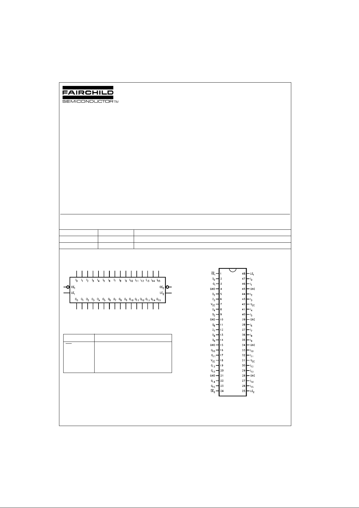
Logic Symbol
Pin Descriptions
Connection Diagram
FACT, Qui et Series , FACT Quiet Series, an d GTO are trademarks of Fairchild Semiconductor Corporation.
Order Number Package Number Package Description
74ACTQ16373MEA MS48A 48-Lead Small Shrink Outline Package (SSOP), JEDEC MO-118, 0.300” Wide
74ACTQ16373MTD MTD48 48-Lead Thin Shrink Small Outline Package (TSSOP), JEDEC MO-153, 6.1mm Wide
Pin Names Description
OE
n
Output Enable Input (Active LOW)
LE
n
Latch Enable Input
I
0–I15
Inputs
O
0–O15
Outputs
www.fairchildsemi.com 2
74ACTQ16373
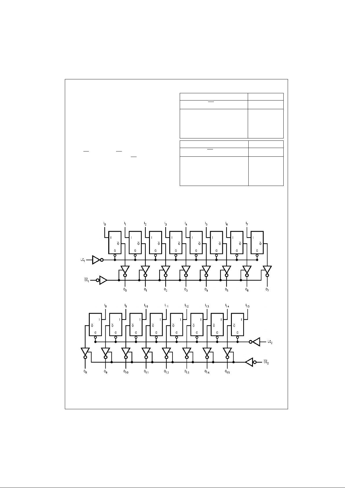
Functional Description
The ACTQ16373 contain s sixteen D-type latches with 3STATE standard outputs. The device is byte controlled with
each byte functioning identically, but independent of the
other. Control pins can be shorted together to obt ain full
16-bit operation. The following description applies to each
byte. When the Latch E nable (LE
n
) input is HIGH, data on
the D
n
enters the latches. In this condition the la tches are
transparent, i.e., a latch output will change states each time
its D input changes. When LE
n
is LOW, the latches store
information that was prese nt on the D inputs a setup time
preceding the HIGH-to-LOW transition of LE
n
. The 3-
STATE standard outputs are controlled by the Output
Enable (OE
n
) input. When OEn is LOW, the standard out-
puts are in the 2-state mode. When OE
n
is HIGH, the stan-
dard outputs are in the high impedance mode but this does
not interfere with entering new data into the latches.
Tr uth Tables
H = HIGH Voltage Level
L = LOW Voltage Level
X = Immaterial
Z = High Impedance
Previous = previous output prior to HIGH-to-LOW transition of LE
Logic Diagrams
Inputs Outputs
LE
1
OE
1
I0–I
7
O0–O
7
X H X Z
H L L L
H L H H
L L X (Previous)
Inputs Outputs
LE
2
OE
2
I8–I
15
O8–O
15
X H X Z
H L L L
H L H H
L L X (Previous)
3 www.fairchildsemi.com
74ACTQ16373
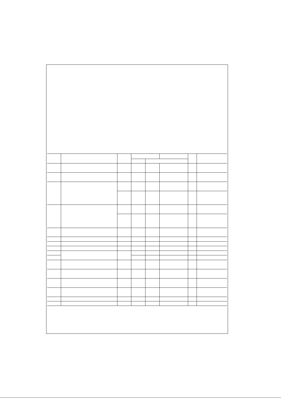
Absolute Maximum Ratings(Note 1) Recommended Operating
Conditions
Note 1: Absolute maximu m rating s are thos e values be yond wh ich dam-
age to the device may occur. The databook specifications should be met,
without exception to ensure th at th e system design is reliable over its power
supply, temperature, and output/input loading variables. Fairchild does not
recommend operation of FACT circuits outside da t abook specifications.
DC Electrical Characteristics
Note 2: All outputs loaded; thresholds associated with output under test.
Note 3: Maximum test duration 2.0 ms; one output loaded at a time.
Note 4: Worst case package
Note 5: Maximum number of outputs that can switch simultaneously is n. (n − 1) outpu t s are switched LOW and one out put held LOW.
Note 6: Maximum number of outputs that can switch simultaneously is n. (n − 1) outpu t s are switched HIGH and one output held HIGH.
Note 7: Max number of data input s (n ) s w it c hing, (n − 1) input switching 0 V t o 3V. Input under te st s w it c hing 3V to threshold (V
ILD
)
Supply Voltage (VCC) −0.5V to +7.0V
DC Input Diode Current (I
IK
)
V
I
= −0.5V −20 mA
V
I
= VCC + 0.5V +20 mA
DC Output Diode Current (I
OK
)
V
O
= −0.5V −20 mA
V
O
= VCC + 0.5V +20 mA
DC Output Voltage (V
O
) −0.5V to VCC + 0.5V
DC Output Source/Sink Current (I
O
) +50 mA
DC V
CC
or Ground Current +50 mA
per Output Pin
Junction Temp erature +140°C
Storage Temperature −65°C to+150°C
Supply Voltage (V
CC
) 4.5V to 5.5V
Input Voltage (V
I
) 0V to V
CC
Output Voltage (VO) 0V to V
CC
Operating Temperature (TA) −40°C to +85°C
Minimum Input Edge Rate (∆V/∆t) 125 mV/ns
V
IN
from 0.8V to 2.0V
V
CC
@ 4.5V, 5.5V
Symbol Parameter
V
CC
TA = +25°C TA = −40°C to +85°C
Units Conditions
(V) Typ Guaranteed Limits
V
IH
Minimum HIGH 4.5 1.5 2.0 2.0
V
V
OUT
= 0.1V
Input Voltage 5.5 1.5 2.0 2.0 or VCC − 0.1V
V
IL
Maximum LOW 4.5 1.5 0.8 0.8
V
V
OUT
= 0.1V
Input Voltage 5.5 1.5 0.8 0.8 or VCC − 0.1V
V
OH
Minimum HIGH 4.5 4.49 4.4 4.4
VI
OUT
= −50 µA
Output Voltage 5.5 5.49 5.4 5.4
VIN = VIL or V
IH
4.5 3.86 3.76 V IOH = −24 mA
5.5 4.86 4.76 IOH = −24 mA (Note 2)
V
OL
Maximum LOW 4.5 0.001 0.1 0.1
V I
OUT
= 50 µA
Output Voltage 5.5 0.001 0.1 0.1
VIN = VIL or V
IH
4.5 0.36 0.44 V IOL = 24 mA
5.5 0.36 0.44 I
OL
= 24 mA (Note 2)
I
OZ
Maximum 3-STATE
5.5 ± 0.5 ± 5.0 µA
VI = VIL, V
IH
Leakage Current VO = VCC, GND
I
IN
Maximum Input Leakage Current 5.5 ± 0.1 ± 1.0 µA VI = VCC, GND
I
CCT
Maximum ICC/Input 5.5 0.6 1.5 mA VI = VCC − 2.1V
I
CC
Max Quiescent Supply Current 5.5 8.0 80.0 µA VIN = VCC or GND
I
OLD
Minimum Dynamic 5.5 75 mA V
OLD
= 1.65V Max
I
OHD
Output Current (Note 3) −75 mA V
OHD
= 3.85V Min
V
OLP
Quiet Output
5.0 0.5 0.8 V
Figure 1, Figure 2
Maximum Dynamic V
OL
(Note 5)(Note 6)
V
OLV
Quiet Output
5.0 −0.5 −1.0 V
Figure 1, Figure 2
Minimum Dynamic V
OL
(Note 5)(Note 6)
V
OHP
Maximum Overshoot 5.0 VOH + 1.0 VOH + 1.5 V Figure 1, Figure 2
(Note 4)(Note 6)
V
OHV
Minimum VCC Droop 5.0 VOH − 1.0 VOH − 1.8 V Figure 1, Figure 2
(Note 4)(Note 6)
V
IHD
Minimum HIGH Dynamic Input Voltage Level 5.0 1.7 2.0 V (Note 4)(Note 7)
V
ILD
Maximum LOW Dynamic Input Voltage Level 5.0 1.2 0.8 V (Note 4)(Note 7)
 Loading...