

Fairchild Semiconductor 74ACTQ153SCX, 74ACTQ153SC, 74ACTQ153PC, 74ACTQ153CW Datasheet
July 1990
Revised May 1999
74ACTQ153 Quiet Series Dual 4-Input Multiplexer
© 1999 Fairchild Semiconductor Corporation DS010244.prf www.fairchildsemi.com
74ACTQ153
Quiet Series Dual 4-Input Multiplexer
General Description
The ACTQ153 is a high-speed dual 4-input multiplexer with
common select inputs and individual enable inputs for each
section. It can select two lines of data fro m four sources.
The two buffered outputs present data in the true (noninverted) form. In addition to multiplexer operation, the
ACTQ153 can act as a function generat or and generate
any two functions of three variables.
Features
■ Outputs source/sink 24 mA
■ ACTQ153 has TTL-compatible inputs
■ Guaranteed simultaneous switching noise level and
dynamic threshold performance
■ Guarante ed pin-to-pi n skew AC per formance
■ Improved latch-up immunity
Ordering Code:
Device also available in Tape and Reel. Specify by appending s uffix let te r “X” to the ordering code.
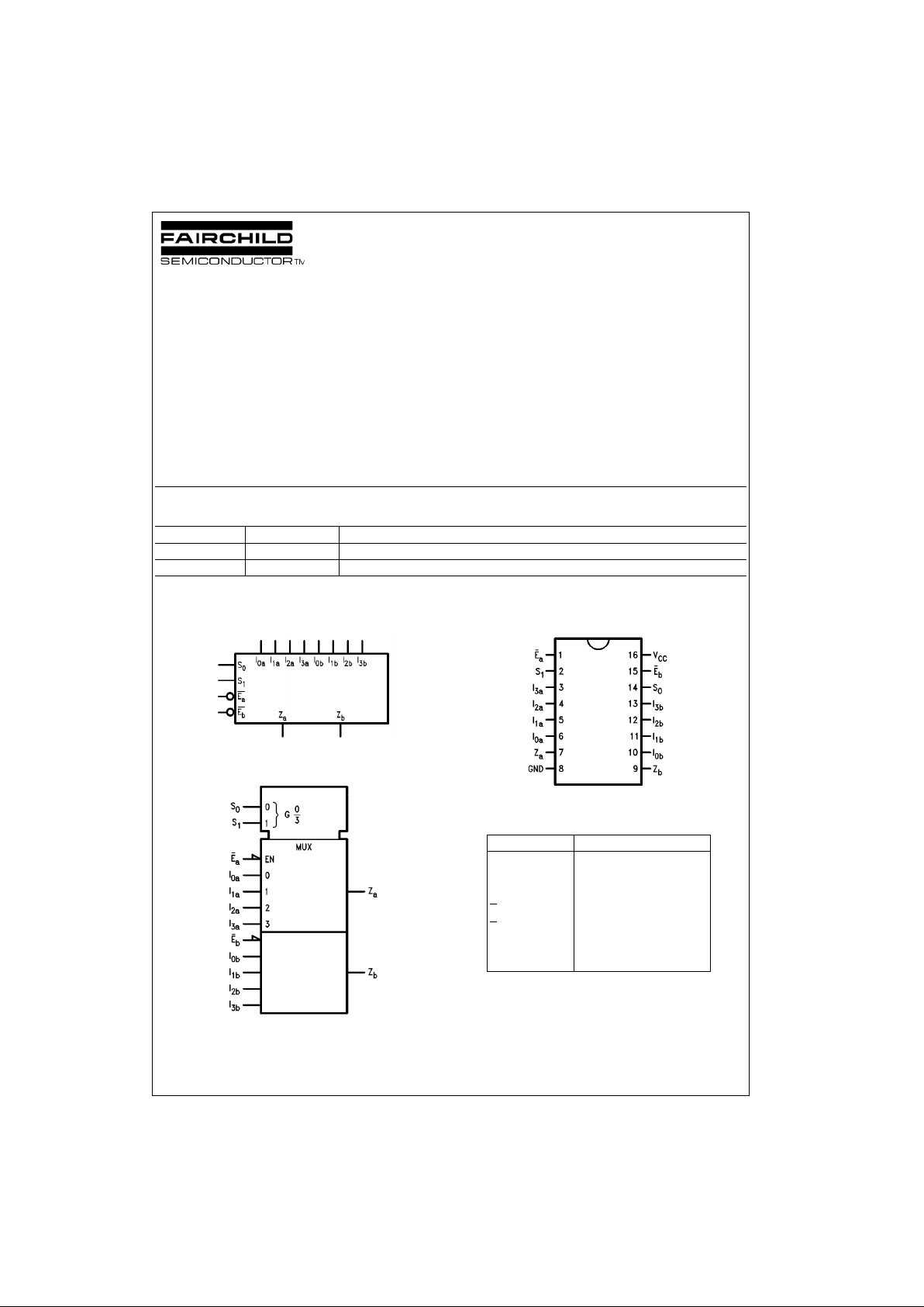
Logic Symbols
IEEE/IEC
Connection Diagram
Pin Descriptions
FACT, FACT Quiet Serie s , and GTO are trademarks of F airchild Semiconductor Corporation.
Order Number Package Number Package Description
74ACTQ153SC M20B 20-Lead Small Outline Integrated Circuit (SOIC), JEDEC MS-013, 0.300 Wide
74ACTQ153PC N20A 20-Lead Plastic Dual-In-Line Package (PDIP), JEDEC MS-001, 0.300 Wide
Pin Names Description
I
0a
- 1
3a
Side A Data Inputs
I
0b
- 1
3b
Side B Data Inputs
S
0
, S
1
Common Select Inputs
E
a
Side A Enable Input
E
b
Side B Enable Input
Z
a
Side A Output
Z
b
Side B Output
www.fairchildsemi.com 2
74ACTQ153
Functional Description
The ACTQ153 is a dual 4-input multip lexer. It can select
two bits of data from up to four sources under the control of
the common Select inputs (S
0
, S1). The two 4-input multi-
plexer circuits have indi vi d ua l ac t iv e- L OW E n ab les ( E
a
, Eb)
which can be used to strobe the outputs independently.
When the Enables (E
a
, Eb) are HIGH, the corre sponding
outputs (A
z
, Zb) are forced LOW. The ACTQ153 is the logic
implementation of a 2-pole , 4-position switch, where the
position of the switch is determined by the logic levels supplied to the Select input s. The logic equatio ns for the outputs are shown below.
Z
a
= Ea • (I0a • S1 • S0 + I1a • S1 • S0 +
I
2a
• S1 •S0 + I3a • S1 • S0)
Z
b
= Eb • (I0b • S1 • S0 • I1b • S1 • S0 +
I
2b
• S1 • S0 +I3b • S1 • S0)
Tr uth Table
H = HIGH Voltage Level
L = LOW Voltage Level
X = Immaterial
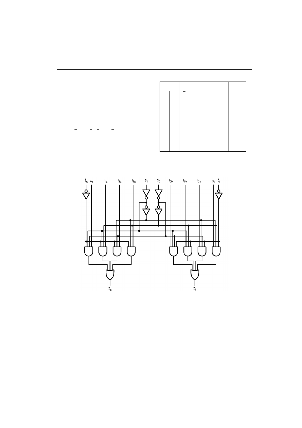
Logic Diagram
Please note that this diagram is provided only f or t he understanding of lo gic operations and should not be used to estimate propagation delays.
Select
Inputs
Inputs (a or b) Outputs
S
0S1
E I0I1I2I
3
Z
XXHXXXX L
LLLLXXX L
LLLHXXX H
HLLXLXX L
HLLXHXX H
LHLXXLX L
LHLXXHX H
HHLXXXL L
HHLXXXH H
3 www.fairchildsemi.com
74ACTQ153
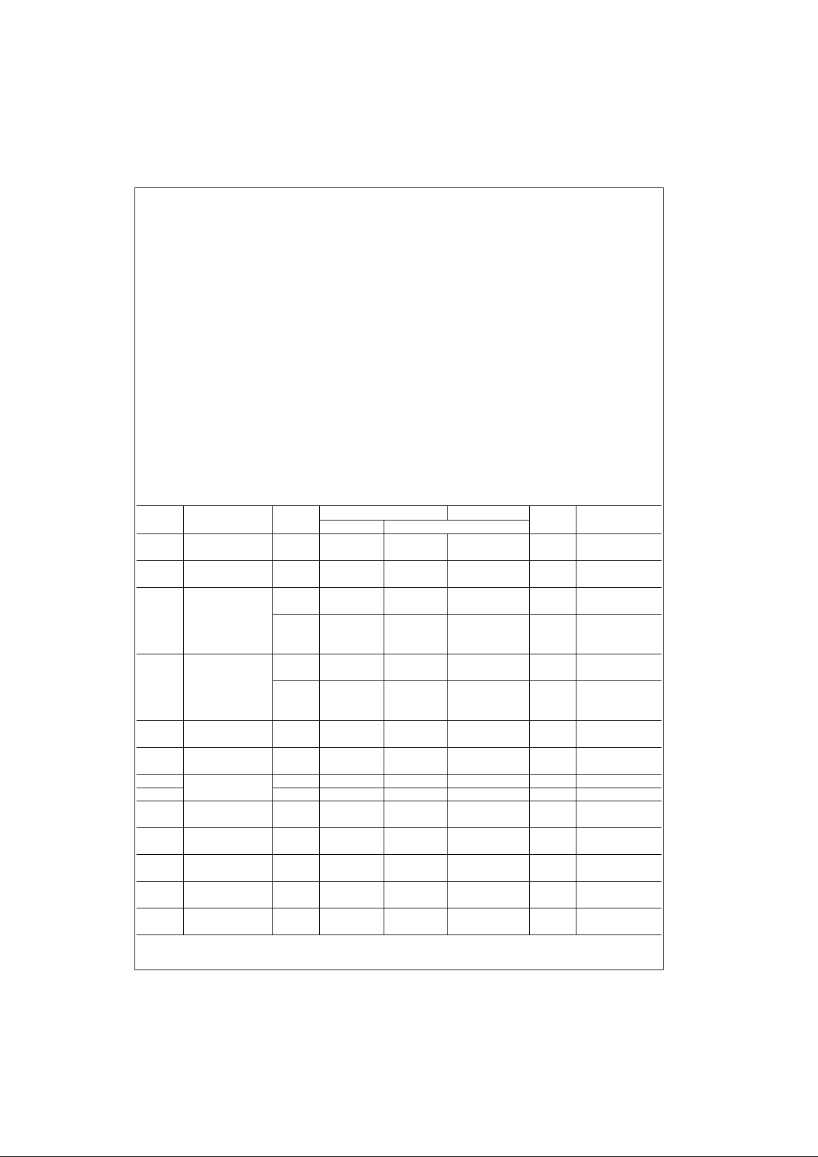
Absolute Maximum Ratings(Note 1) Recommended Operating
Conditions
Note 1: Absolute maximum ratings are those values beyond which damage
to the device may occur. The databook specifications should be met, without exception, to ensure that the system design is reliable over its power
supply, temperature, and ou tput/inp ut load ing vari ables. Fairchild does n ot
recommend operat ion of FACT circuits outside dat abook specifications.
DC Electrical Characteristics
Note 2: All outputs loaded; thresholds on inpu t as s oc iated with output under te s t .
Note 3: Maximum test duration 2.0 ms, one output loaded at a time.
Supply Voltage (VCC) −0.5V to +7.0V
DC Input Diode Current (I
IK
)
V
I
= −0.5V −20 mA
V
I
= VCC + 0.5V +20 mA
DC Input Voltage (V
I
) −0.5V to VCC + 0.5V
DC Output Diode Current (I
OK
)
V
O
= −0.5V −20 mA
V
O
= VCC + 0.5V +20 mA
DC Output Voltage (V
O
) −0.5V to VCC + 0.5V
DC Output Source
or Sink Current (I
O
) ±50 mA
DC V
CC
or Ground Current
per Output Pin (I
CC
or I
GND
) ±50 mA
Storage Temperature (T
STG
) −65°C to +150°C
DC Latch-Up Source or Sink Current ±300 mA
Junction Temperature (T
J
)
PDIP 140°C
Supply Voltage (V
CC
) 4.5V to 5.5V
Input Voltage (V
I
)0V to V
CC
Output Voltage (VO)0V to V
CC
Operating Temperature (TA) −40°C to +85°C
Minimum Input Edge Rate ∆V/∆t
V
IN
from 0.8V to 2.0V
V
CC
@ 4.5V, 5.5V 125 mV/ns
Symbol Parameter
V
CC
TA = +25°CT
A
= −40°C to +85°C
Units Conditions
(V) Typ Guaranteed Limits
V
IH
Minimum HIGH Level 4.5 1.5 2.0 2.0
V
V
OUT
= 0.1V
Input Voltage 5.5 1.5 2.0 2.0 or VCC − 0.1V
V
IL
Maximum LOW Level 4.5 1.5 0.8 0.8
V
V
OUT
= 0.1V
Input Voltage 5.5 1.5 0.8 0.8 or VCC − 0.1V
V
OH
Minimum HIGH Level 4.5 4.49 4.4 4.4
V
I
OUT
= −50 µA
Output Voltage 5.5 5.49 5.4 5.4
V
VIN = VIL or VIH
4.5 3.86 3.76 IOH = −24 mA
5.5 4.86 4.76 IOH = −24 mA (Note 2)
V
OL
Maximum LOW Level 4.5 0.001 0.1 0.1
V
I
OUT
= 50 µA
Output Voltage 5.5 0.001 0.1 0.1
V
VIN = VIL or V
IH
4.5 0.36 0.44 IOL = 24 mA
5.5 0.36 0.44 IOL = 24 mA (Note 2)
I
IN
Maximum Input
5.5 ±0.1 ±1.0 µAVI = VCC, GND
Leakage Current
I
CCT
Maximum
5.5 0.6 1.5 µAVI = VCC − 2.1V
ICC/Input
I
OLD
Minimum Dynamic 5.5 75 mA V
OLD
= 1.65V Max
I
OHD
Output Current (Note 3) 5.5 −75 mA V
OHD
= 3.85V Min
I
CC
Maximum Quiescent
5.5 8.0 80.0 µA
VIN = V
CC
Supply Current or GND
V
OLP
Maximum HIGH Level
5.0 1.1 1.5 V
Figure 1Figure 2
Output Noise (Note 4)(Note 5)
V
OLV
Maximum LOW Level
5.0 −0.6 −1.2 V Figure 1Figure 2
Output Noise
V
IHD
Minimum HIGH Level
5.0 1.9 2.2 V (Note 4)(Note 6)
Dynamic Input Voltage
V
ILD
Maximum LOW Level
5.0 1.2 0.8 V (Note 4)(Note 6)
Dynamic Input Voltage
 Loading...