

Fairchild Semiconductor 74ACTQ14SCX, 74ACTQ14SC, 74ACTQ14PC, 74ACTQ14MTCX, 74ACTQ14MTC Datasheet
...
© 1999 Fairchild Semiconductor Corporation DS010911 www.fairchildsemi.com
March 1991
Revised November 1999
74ACTQ14 Quiet Series Hex Inverter with Schmitt Trigger Input
74ACTQ14
Quiet Series Hex Inverter with Schmitt Trigger Input
General Description
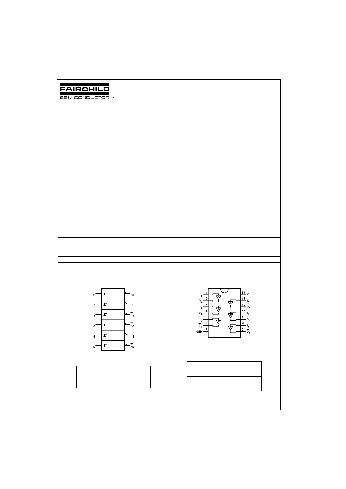
The ACTQ14 contains six inverter gates each with a
Schmitt trigger input. They are capable of transforming
slowly changing input sign als into sharply defined, jitterfree output signals. In ad dition, they have a great er noise
margin than conventional inverters.
The ACTQ14 utilizes Fairchild Quiet Series Technology
to guarantee quiet output switchin g and improve dy namic
threshold performance. FACT Quiet Series features
GTO output control and unde rshoot corre ctor in add ition
to a split ground bus for superior performance.
The ACTQ14 has hysteresis between the positive-going
and negative-going i nput threshold s (typically 1.0 V) which
is determined internally by transistor ratios and is essentially insensitive to temp erature and supply voltage variations.
Features
■ ICC reduced by 50%
■ Guaranteed simultaneous switching noise level and
dynamic threshold performan ce
■ Improved latch-up immunity
■ Guarante ed pin-to-pin skew AC performance
■ Outputs source/sink 24 mA
Ordering Code:
Device also available in Tape and Reel. Specify by appending s uffix let te r “X” to the ordering code.
Logic Symbol
IEEE/IEC
Pin Descriptions
Connection Diagram
Function Table
Quiet Series, FACT Quiet Series and GTO are trademarks of Fairchild Semiconductor Corporation.
Order Number Package Number Package Description
74ACTQ14SC M14A 14-Lead Small Outline Integrated Circuit (SOIC), JEDEC MS-120, 0.150” Narrow Body
74ACTQ14MTC MTC14 14-Lead Thin Shrink Small Outline Package (TSSOP), JEDEC MO-153, 4.4mm Wide
74ACTQ14PC N14A 14-Lead Plastic Dual-In-Lead Package (PDIP), JEDEC MS-001, 0.300” Wide
Pin Names Description
I
n
Inputs
O
n
Outputs
Input Output
AO
LH
HL
www.fairchildsemi.com 2
74ACTQ14
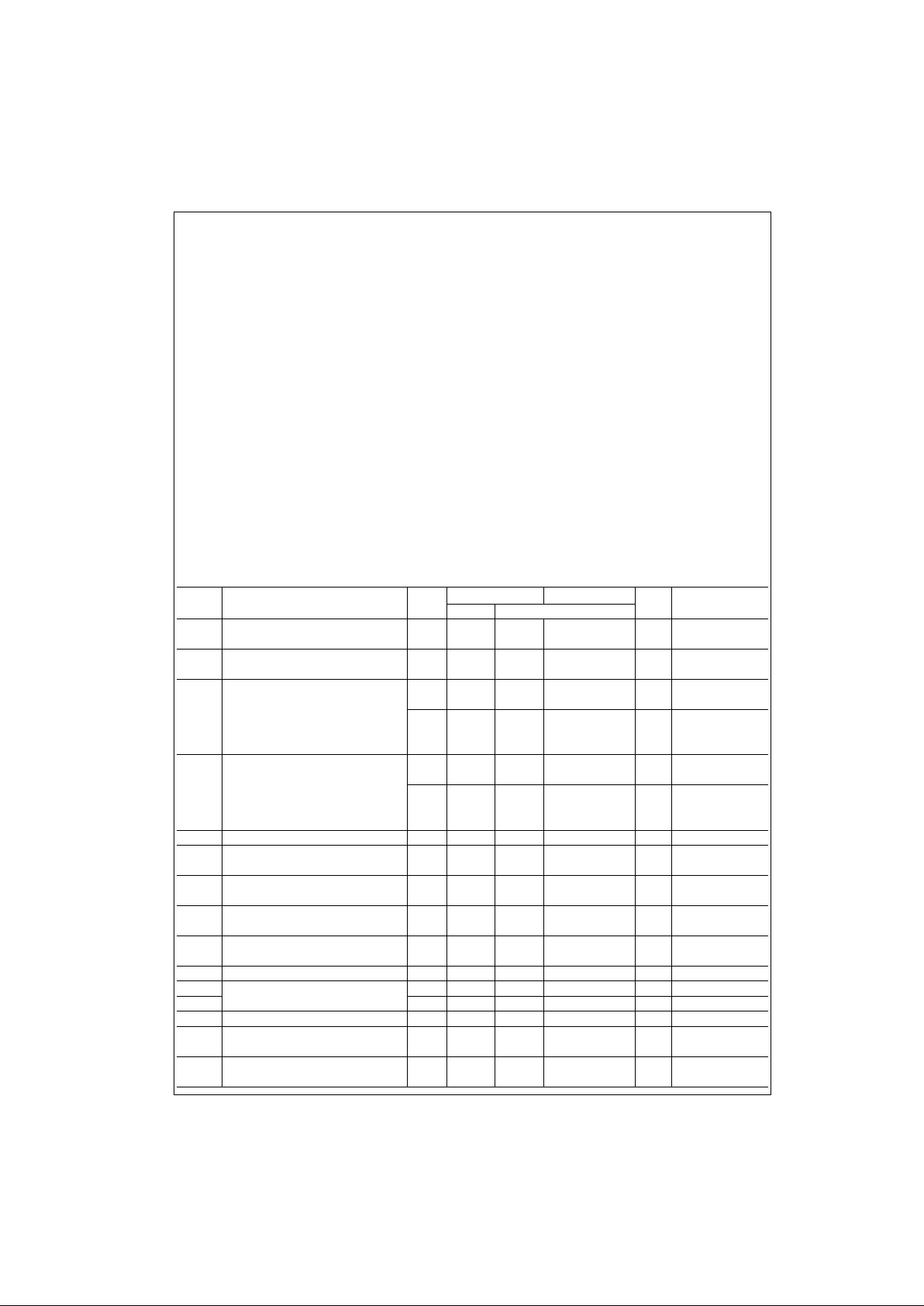
Absolute Maximum Ratings(Note 1) Recommended Operating
Conditions
Note 1: Absolute maximum ratings are those values beyond which damage
to the device may occur. The databook specifications should be met, without exception, to ensure that the system design is reliable over its power
supply, temperature, and ou tput/inp ut loadi ng varia bles. Fairchild does no t
recommend operat ion outside of databook s pecifications.
DC Electrical Characteristics
Supply Voltage (VCC) −0.5V to +7.0V
DC Input Diode Current (I
IK
)
V
I
= −0.5V −20 mA
V
I
= VCC + 0.5V +20 mA
DC Input Voltage (V
I
) −0.5V to VCC + 0.5V
DC Output Diode Current (I
OK
)
V
O
= −0.5V −20 mA
V
O
= VCC + 0.5V +20 mA
DC Output Voltage (V
O
) −0.5V to VCC + 0.5V
DC Output Source
or Sink Current (I
O
) ± 50 mA
DC V
CC
or Ground Current
per Output Pin (I
CC
or I
GND
) ± 50 mA
Storage Temperature (T
STG
) −65°C to +150°C
DC Latch-Up Source
or Sink Current ± 300 mA
Junction Temperature (T
J
)
PDIP 140°C
Supply Voltage (V
CC
) 4.5V to 5.5
Input Voltage (V
I
) 0V to V
CC
Output Voltage (VO) 0V to V
CC
Operating Temperature (TA) −40°C to +85°C
Symbol Parameter
V
CC
T A = +25°CTA = −40°C to +85°C
Units Conditions
(V) Typ Guaranteed Limits
V
IH
Minimum HIGH Level 4.5 1.5 2.0 2.0
V
V
OUT
= 0.1V
Input Voltage 5.5 1.5 2.0 2.0 or VCC − 0.1V
V
IL
Maximum LOW Level 4.5 1.5 0.8 0.8
V
V
OUT
= 0.1V
Input Voltage 5.5 1.5 0.8 0.8 or VCC − 0.1V
V
OH
Minimum HIGH Level 4.5 4.49 4.4 4.4
VI
OUT
= −50 µA
Output Voltage 5.5 5.49 5.4 5.4
V
IN
= VIL or V
IH
4.5 3.86 3.76 V IOH = −24 mA
5.5 4.86 4.76 IOH = −24 mA (Note 2)
V
OL
Maximum LOW Level 4.5 0.001 0.1 0.1
VI
OUT
= 50 µA
Output Voltage 5.5 0.001 0.1 0.1
VIN = VIL or V
IH
4.5 0.36 0.44 V IOL = 24 mA
5.5 0.36 0.44 I
OL
= 24 mA (Note 2)
I
IN
Maximum Input Leakage Current 5.5 ± 0.1 ± 1.0 µAVI = VCC, GND
V
h(max)
Maximum Hysteresis 4.5 1.4 1.4
VTA = Worst Case
5.5 1.6 1.6
V
h(min)
Minimum Hysteresis 4.5 0.4 0.4
VTA = Worst Case
5.5 0.5 0.5
Vt+ Maximum Positive 4.5 2.0 2.0
VTA = Worst Case
Threshold 5.5 2.0 2.0
Vt− Minimum Negative 4.5 0.8 0.8
VTA = Worst Case
Threshold 5.5 0.8 0.8
I
CCT
Maximum ICC/Input 5.5 0.6 1.5 mA VI = VCC − 2.1V
I
OLD
Minimum Dynamic 5.5 75 mA V
OLD
= 1.65V Max
I
OHD
Output Current (Note3) 5.5 −75 mA V
OHD
= 3.85V Min
I
CC
Maximum Quiescent Supply Current 5.5 2.0 20.0 µAVIN = VCC or GND
V
OLP
Quiet Output Maximum
5.0 1.1 1.5 V
Figure 1, Figure 2
Dynamic V
OL
(Note 4)(Note 5)
V
OLV
Quiet Output Minimum
5.0 −0.6 −1.2 V
Figure 1, Figure 2
Dynamic V
OL
(Note 4)(Note 5)
3 www.fairchildsemi.com
74ACTQ14
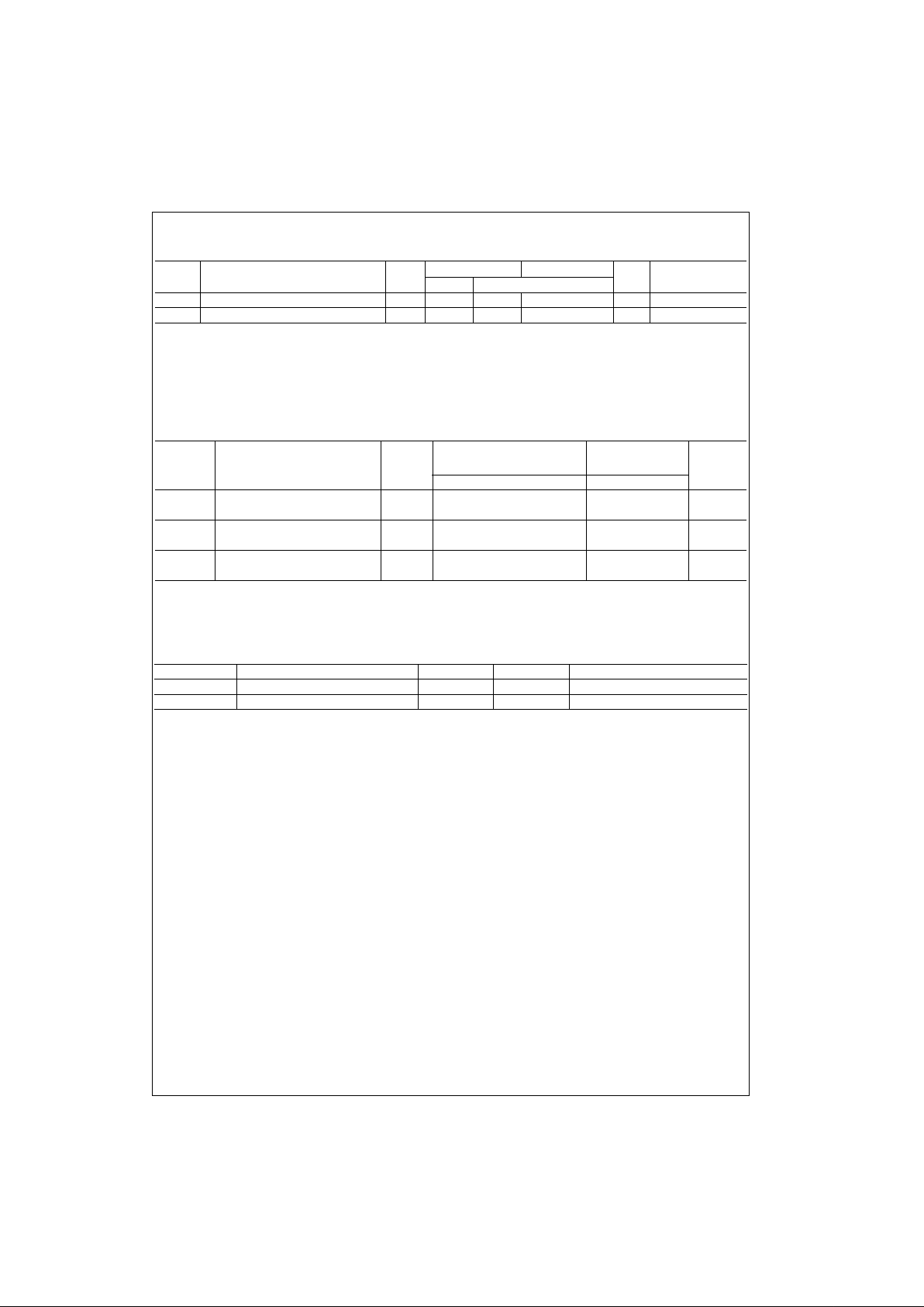
DC Electrical Characteristics (Continued)
Note 2: All outputs loaded; thres holds on input associate d w it h output under test.
Note 3: Maximum test duration 2.0 ms, one output loaded at a time.
Note 4: DIP package.
Note 5: Max number of outputs def ined as (n). Data inputs are 0V to 3V. One output @ GND.
Note 6: Max number of data input s (n ) s w it c hing. (n−1) inputs switching 0V to 3V. Input-under-test switching: 3V to threshold (V
ILD
),
0V to threshold (V
IHD
), f = 1 MHz.
AC Electrical Characteristics
Note 7: Voltage Range 5.0 is 5.0V ± 0.5V.
Note 8: Skew is defined as t he absolute value of t he difference between the actual propagation delay for any two separate outputs of the same device. The
specification applies to any outputs switching in the same direction, either HIGH-to-LOW (t
OSHL
) or LOW-to-HIGH (t
OSLH
). Parameter guaranteed by de s ign.
Capacitance
Symbol Parameter
V
CC
T A = +25°CTA = −40°C to +85°C
Units Conditions
(V) Typ Guaranteed Limits
V
IHD
Minimum HIGH Level Dynamic Input Voltage 5.0 1.9 2.2 V (Note 4)(Note 6)
V
ILD
Maximum LOW Level Dynamic Input Voltage 5.0 1.2 0.8 V (Note 4)(Note 6)
V
CC
TA = +25°CT
A
= −40°C to +85°C
Symbol Parameter (V)
CL = 50 pF CL = 50 pF
Units
(Note 7) Min Typ Max Min Max
t
PLH
Propagation Delay
5.0 3.0 8.0 10.0 3.0 11.0 ns
Data to Output
t
PHL
Propagation Delay
5.0 3.0 8.0 10.0 3.0 11.0 ns
Data to Output
t
OSHL
Output to Output
5.0 0.5 1.0 1.0 ns
t
OSLH
Skew (Note 8)
Symbol Parameter Typ Units Conditions
C
IN
Input Capacitance 4.5 pF VCC = OPEN
C
PD
Power Dissipation Capacitance 80 pF VCC = 5.0V
 Loading...