

Fairchild Semiconductor 74ACTQ10SCX, 74ACTQ10SC, 74ACTQ10PC, 74ACTQ10MTCX, 74ACTQ10MTC Datasheet
...
© 2000 Fairchild Semiconductor Corporation DS010892 www.fairchildsemi.com
August 1990
Revised August 2000
74ACTQ10 Quiet Series
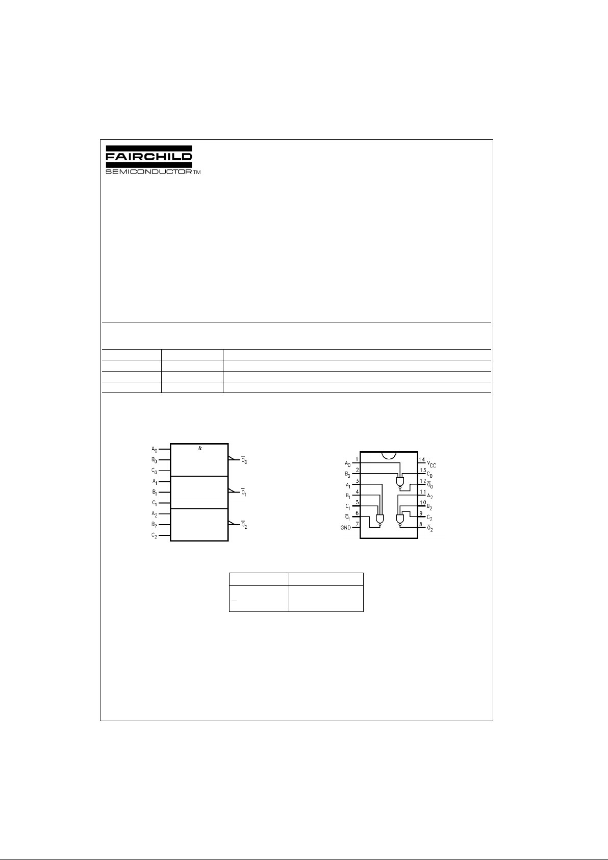
Tripl e 3-Input NAND Gate
74ACTQ10
Quiet Series
Triple 3-Input NAND Gate
General Description
The ACTQ10 contains three, 3-in put NAND gat es and utilizes Fairchild FACT Quiet Series
technology to guaran-
tee quiet output switching and impr ove d dyna mic thr esh old
performance. FACT Quiet Series features GTO
output
control and undershoot corrector in addition to a split
ground bus for superior ACMOS performance.
Features
■ ICC reduced by 50%
■ Guaranteed simultaneous switching noise level and
dynamic threshold performan ce
■ Improved latch-up immunity
■ Outputs source/sink 24 mA
■ ACTQ 10 has TTL-compatible in put s
Ordering Code:
Device also available in Tape and Reel. Specify by appending s uffix let te r “X” to the ordering code.
Logic Symbol
IEEE/IEC
Connection Diagram
Pin Descriptions
FACT, Qui et Series , FACT Quiet Series, an d GTO are trademarks of Fairchild Semiconductor Corporation.
Order Number Package Number Package Description
74ACTQ10SC M14A 14-Lead Small Outline Integrated Circuit (SOIC), JEDEC MS-012, 0.150” Narrow Body
74ACTQ10MTC MTC14 14-Lead Thin Shrink Small Outline Package (TSSOP), JEDEC MO-153, 4.4mm Wide
74ACTQ10PC N14A 14-Lead Plastic Dual-In-Line Package (PDIP), JEDEC MS-001, 0.300” Wide
Pin Names Descriptions
A
n
, Bn, C
n
Inputs
O
n
Outputs
www.fairchildsemi.com 2
74ACTQ10
Absolute Maximum Ratings(Note 1) Recommended Operating
Conditions
Note 1: Absolute maximum ratings are values beyond which damage to the
device may occur. The databo ok specifications should be met, with out
exception, to ensure that the system design is reliable over its power supply, temperature, and output/input loading variables. Fairchild does not recommend operation outside of databook sp ec if ic ations.
DC Electrical Characteristics
Note 2: All outputs loaded; thresholds on input assoc iat ed with output under tes t.
Note 3: Maximum test duratio n 2. 0 ms, one output loaded at a time.
Note 4: DIP Package .
Note 5: Max number of output s d ef ined as (n). Data inputs are 0V to 3V. One output @ GND.
Note 6: Max number of data inputs (n) switching. (n-1) inputs switching 0V to 3V. Input-under -te s t swit c hing:
3V to threshold (V
ILD
), 0V to threshold (V
IHD
), f = 1MHZ.
Supply Voltage (VCC) −0.5V to +7.0V
DC Input Diode Current (I
IK
)
V
I
= −0.5V −20 mA
V
I
= VCC + 0.5V +20 mA
DC Input Voltage (V
I
) −0.5V to VCC + 0.5V
DC Output Diode Current (I
OK
)
V
O
= −0.5V −20 mA
V
O
= VCC + 0.5V +20 mA
DC Output Voltage (V
O
) −0.5V to VCC + 0.5V
DC Output Source
or Sink Current (I
O
) ± 50 mA
DC V
CC
or Ground Current
per Output Pin (I
CC
or I
GND
) ± 50 mA
Storage Temperature (T
STG
) −65°C to +150°C
DC Latch-Up Source or Sink Current
± 300 mA
Junction Temperature (T
J
)
PDIP 140
°C
Supply Voltage (V
CC
) 4.5V to 5.5V
Input Voltage (V
I
) 0V to V
CC
Output Voltage (VO) 0V to V
CC
Operating Temperature (TA) −40°C to +85°C
Minimum Input Edge Rate (
∆V/∆t) 125 mV/ns
V
IN
from 0.8V to 2.0V
V
CC
@ 4.5V, 5.5V
Symbol Parameter
V
CC
TA = +25°CTA = −40°C to +85°C
Units Conditions
(V) Typ Guaranteed Limits
V
IH
Minimum HIGH Level 4.5 1.5 2.0 2.0
V
V
OUT
= 0.1V
Input Voltage 5.5 1.5 2.0 2.0 or VCC − 0.1V
V
IL
Maximum LOW Level 4.5 1.5 0.8 0.8
V
V
OUT
= 0.1V
Input Voltage 5.5 1.5 0.8 0.8 or VCC − 0.1V
V
OH
Minimum HIGH Level 4.5 4.49 4.4 4.4
VI
OUT
= −50 µA
Output Voltage 5.5 5.49 5.4 5.4
VIN = VILor V
IH
4.5 3.86 3.76 V IOH = − 24 mA
5.5 4.86 4.76 I
OH
= − 24 mA (Note 2)
V
OL
Maximum LOW Level 4.5 0.001 0.1 0.1
VI
OUT
= 50 µA
Output Voltage 5.5 0.001 0.1 0.1
VIN = VILor V
IH
4.5 0.36 0.44 V IOL = 24 mA
5.5 0.36 0.44 IOL = 24 mA (Note 2)
I
IN
Maximum Input Leakage Current 5.5 ± 0.1 ± 1.0 µAVI = VCC, GND
I
CCT
Maximum ICC/Input 5.5 0.6 1.5 mA VI = VCC − 2.1V
I
OLD
Minimum Dynamic 5.5 75 mA V
OLD
= 1.65V Max
I
OHD
Output Current (Note 3) 5.5 −75 mA V
OHD
= 3.85V Min
I
CC
Maximum Quiescent Supply Current 5.5 2.0 20.0 µAVIN = VCC or GND
V
OLP
Quiet Output
5.0 1.1 1.5 V
Figures 1, 2
Maximum Dynamic V
OL
(Note 4)(Note 5)
V
OLV
Quiet Output
5.0 −0.6 −1.2 V
Figures 1, 2
Minimum Dynamic V
OL
(Note 4)(Note 5)
V
IHD
Minimum HIGH Level Dynamic Input Voltage 5.0 1.9 2.2 V (Note 4)(Note 6)
V
ILD
Maximum LOW Level Dynamic Input Voltage 5.0 1.2 0.8 V (Note 4)(Note 6)
3 www.fairchildsemi.com
74ACTQ10
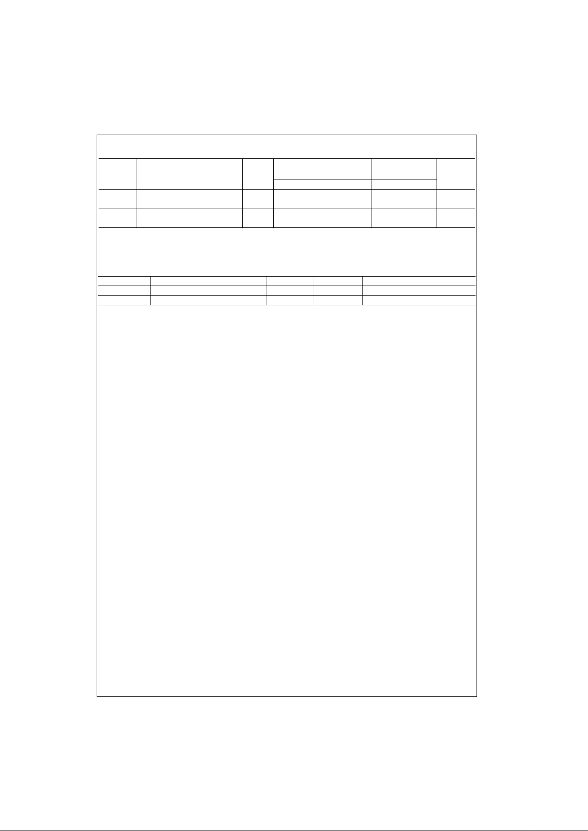
AC Electrical Characteristics
Note 7: Voltage Range 5.0 is 5.0V ± 0.5V.
Note 8: Skew is defined as t he absolute value of t he difference between the actual propagation delay for any two separate outputs of the same device. The
specification applies to any outputs switching in the same direction, either HIGH-to-LOW (t
OSHL
) or LOW-to-HIGH (t
OSLH
). Parameter guaranteed by design.
Capacitance
V
CC
TA = +25°CT
A
= −40°C to +85°C
Symbol Parameter (V)
C
L
= 50 pF CL = 50 pF
Units
(Note 7) Min Typ Max Min Max
t
PLH
Propagation Delay 5.0 2.0 6.0 7.5 2.0 8.5 ns
t
PHL
Propagation Delay 5.0 2.0 6.0 7.5 2.0 8.5 ns
t
OSHL
Output to Output
5.0 0.5 1.0 1.0 ns
t
OSLH
Skew (Note 8)
Symbol Parameter Typ Units Conditions
C
IN
Input Capacitance 4.5 pF VCC = OPEN
C
PD
Power Dissipation Capacitance 85 pF VCC = 5.0V
 Loading...