Fairchild Semiconductor 74ACT18825SSCX, 74ACT18825SSC, 74ACT18825MTDX, 74ACT18825MTD Datasheet

© 1999 Fairchild Semiconductor Corporation DS0500292 www.fairchildsemi.com
August 1999
Revised October 1999
74ACT18825 18-Bit Buffer/Line Driver with 3-STATE Outputs
74ACT18825
18-Bit Buffer/Line Driver with 3-STATE Outputs
General Description
The ACT18825 contains eighteen non-inverting buffers
with 3-STATE outputs designed to be employed as a memory and address driver, clock driver, or bus oriented transmitter/receiver. The device is byte controlled. Each byte
has separate 3-STATE control inputs which can be shorted
together for full 18-bit operation.
Features
■ Broadside pinout allows for easy board layout
■ Separate control logic for each byte
■ Extra data width for wider address/data p aths or buses
carrying parity
■ Outputs source/sink 24 mA
■ TTL-compatible inputs
Ordering Code:
Device also available in Tape and Reel. Specify by appending s uffix let te r “X” to the ordering code.
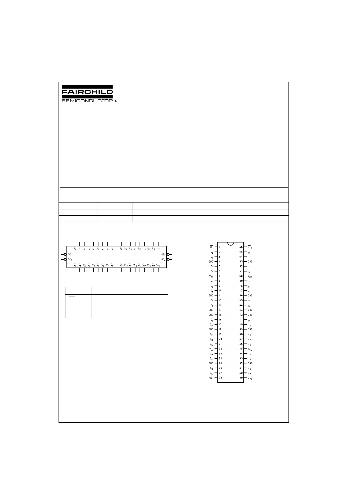
Logic Symbol
Pin Descriptions
Connection Diagram
FACT, FACT Quiet Series and GTO are trademarks of Fairc hild Semiconductor C orporation.
Order Number Package Number Package Description
74ACT18825SSC MS56A 56-Lead Shrink Small Outline Package (SSOP), JEDEC MO-118, 0.300” Wide
74ACT18825MTD MTD56 56-Lead Thin Shrink Small Outline Package (TSSOP), JEDEC MO-153, 6.1mm Wide
Pin Names Description
OE
n
Output Enable Input (Active LOW)
I
0–I17
Inputs
O
0–O17
Outputs

www.fairchildsemi.com 2
74ACT18825
Functional Description
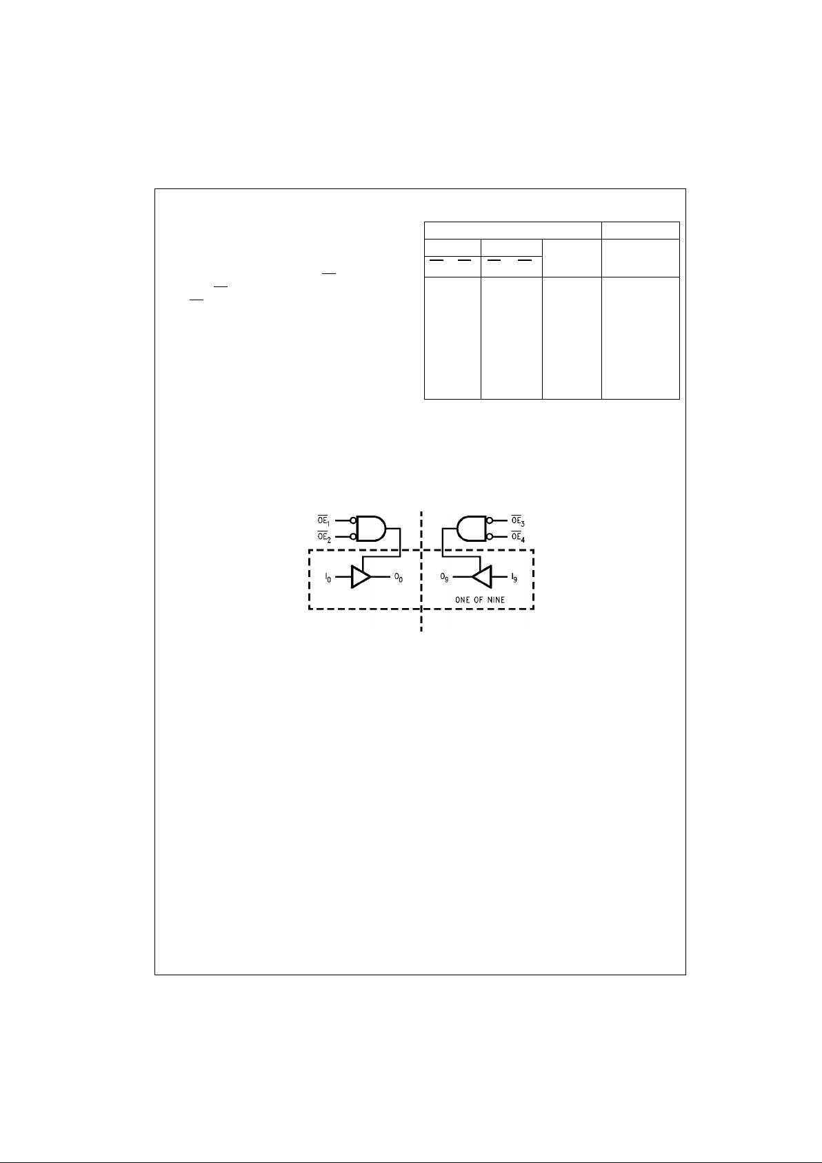
The ACT18825 contains eighteen non-inverting buffers
with 3-STATE standard outputs. Th e device is byte controlled with each by te functioning identically, but independently of the other. The control pins may be shorted
together to obtain full 8-bit operation. The 3-STATE outputs
are controlled by an Output Enabl e (OE
n
) input for each
byte. When OE
n
is LOW, the outputs are in 2-state mode.
When OE
n
is HIGH, the outputs are in the high impedance
mode, but this do es not interfere with enteri ng new data
into the inputs.
Tr uth Table
H = HIGH Voltage Level
L = LOW Voltage Level
X = Immaterial
Z = HIGH Impedance
Logic Diagram
Inputs Outputs
Byte 1 (0:8) Byte 2 (8:17)
I
0–I8I9–I17O0–O8O9–O17
OE1OE2OE3OE
4
LLL LHH H H
HXL L XL Z L
XHL L XH Z H
LLH XLX L Z
LLX HHX H Z
HHH HX X Z Z
LLL LLL L L
 Loading...