

Fairchild Semiconductor 2N4403 Datasheet
Discrete POWER & Signal
Technologies
2N4403 / MMBT4403
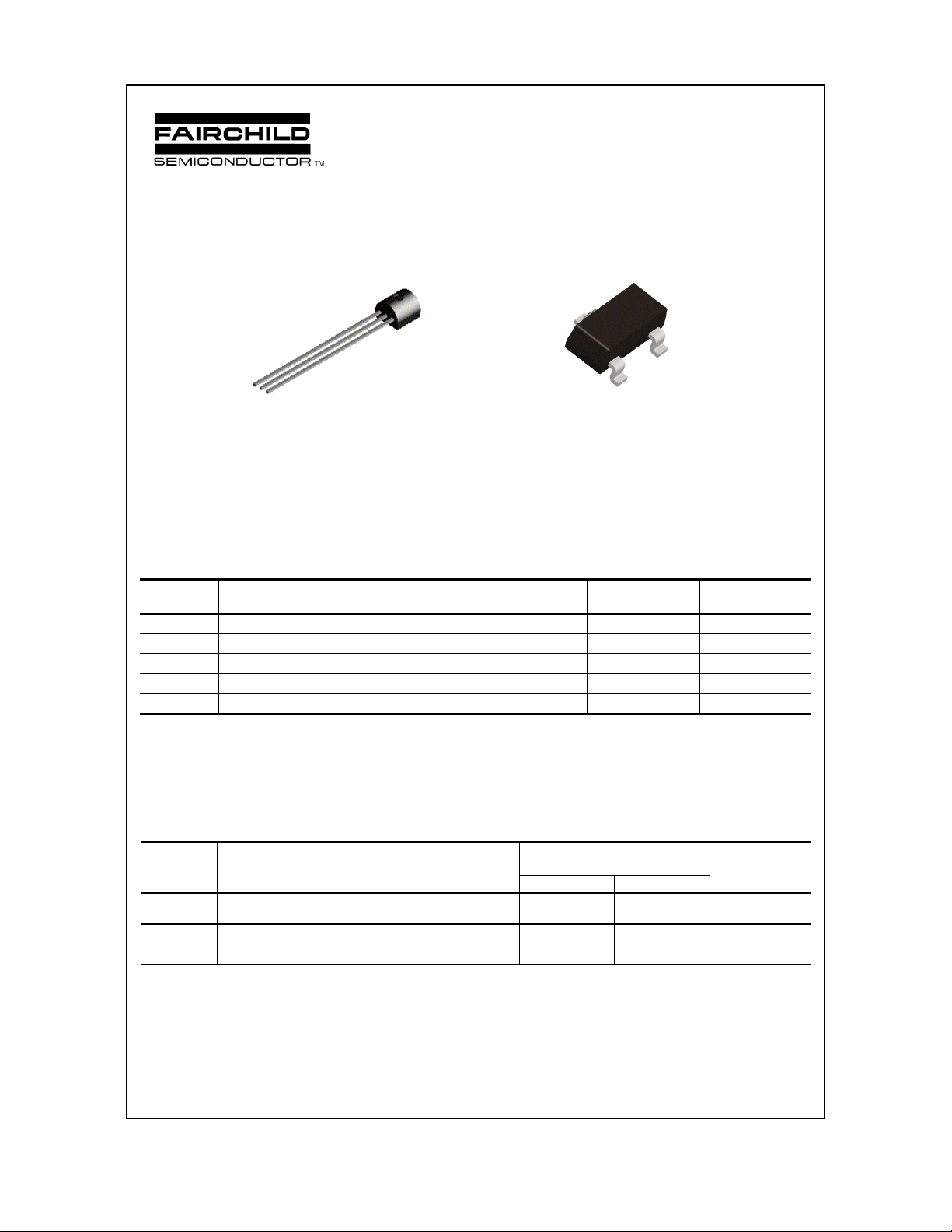
2N4403
C
B
E
TO-92
MMBT4403
C
E
SOT-23
Mark: 2T
B
PNP General Purpose Amplifier
This device is designed for use as a general purpose amplifier
and switch requiring collector currents to 500 mA. Sourced
from Process 63. See PN2907A for characteristics.
Absolute Maximum Ratings* TA = 25°C unless otherwise noted
Symbol Parameter Value Units
V
CEO
V
CBO
V
EBO
I
C
TJ, T
stg
*These ratings are limiting values above which the serviceability of any semiconductor device may be impaired.
NOTES:
1) These ratings are based on a maximum junction temperature of 150 degrees C.
2) These are steady state limits. The factory should be consulted on applications involving pulsed or low duty cycle operations.
Collector-Emitter Voltage 40 V
Collector-Base Voltage 45 V
Emitter-Base Voltage 5.0 V
Collector Current - Continuous 800 mA
Operating and Storage Junction Temperature Range -55 to +150
°C
Thermal Characteristics TA = 25°C unless otherwise noted
Symbol Characteristic Max Units
2N4403 *MMBT4403
P
D
R
θ
JC
R
θ
JA
*Device mounted on FR-4 PCB 1.6" X 1.6" X 0.06."
1997 Fairchild Semiconductor Corporation
Total Device Dissipation
Derate above 25°C
Thermal Resistance, Junction to Case 83.3
Thermal Resistance, Junction to Ambient 200 357 °
625
5.0
350
2.8
mW
mW/°C
°
C/W
C/W
PNP General Purpose Amplifier
(continued)
Electrical Characteristics TA = 25°C unless otherwise noted
Symbol Parameter Test Conditions Min Max Units
OFF CHARACTERISTICS
V
(BR)CEO
V
(BR)CBO
V
(BR)EBO
I
BEX
I
CEX
ON CHARACTERISTICS
h
FE
V
sat
CE(
V
sat
BE(
Collector-Emitter Breakdown
IC = 1.0 mA, IB = 0 40 V
Voltage*
Collector-Base Breakdown Voltage IC = 0.1 mA, IE = 0 45 V
Emitter-Base Breakdown Voltage IE = 0.1 A, IC = 0 5.0 V
Base Cutoff Current VCE = 35 V, V
Collector Cutoff Current VCE = 35 V, V
DC Current Gain IC = 0.1 mA, VCE = 1.0 V
I
= 1.0 mA, VCE = 1.0 V
C
IC = 10 mA, VCE = 1.0 V
= 150 mA, VCE = 2.0 V*
I
C
IC = 500 mA, VCE = 2.0 V*
Collector-Emitter Saturation
)
Voltage*
Base-Emitter Saturation Voltage IC = 150 mA, IB = 15 mA*
)
IC = 150 mA, IB = 15 mA
= 500 mA, IB = 50 mA
I
C
IC = 500 mA, IB = 50 mA
= 0.4 V 0.1
EB
= 0.4 V 0.1
BE
30
60
100
100
20
0.75 0.95
300
0.4
0.75
1.3
µ
µ
V
V
V
V
2N4403 / MMBT4403
A
A
SMALL SIGNAL CHARACTERISTICS
f
T
C
cb
C
eb
h
ie
h
re
h
fe
h
oe
Current Gain - Bandwidth Product IC = 20 mA, VCE = 10 V,
Collector-Base Capacitance VCB = 10 V, IE = 0,
Emitter-Base Capacitance VBE = 0.5 V, IC = 0,
Input Impedance IC = 1.0 mA, VCE = 10 V,
Voltage Feedback Ratio IC = 1.0 mA, VCE = 10 V,
Small-Signal Current Gain IC = 1.0 mA, VCE = 10 V,
Out p u t A dmi tt a n c e IC = 1.0 mA, VCE = 10 V,
SWITCHING CHARACTERISTICS
t
d
t
r
t
s
t
f
De lay T ime VCC = 30 V, IC = 150 mA, 15 ns
Rise Time IB1 = 15 mA 20 ns
Storage Time VCC = 6.0 V, IC = 150 mA 225 ns
Fall Time IB1 = IB2 = 15 mA 30 ns
*Pulse Test: Pulse Width ≤ 300 µs, Duty Cycle ≤ 2.0%
f = 100 MHz
f = 140 kHz
f = 140 kHz
f = 1.0 kHz
f = 1.0 kHz
f = 1.0 kHz
f = 1.0 kHz
200 MHz
8.5 pF
30 pF
1.5 15
0.1 8.0
k
x 10
Ω
60 500
1.0 100 µ
mhos
-4
 Loading...