

Fairchild Semiconductor 2N4126 Datasheet
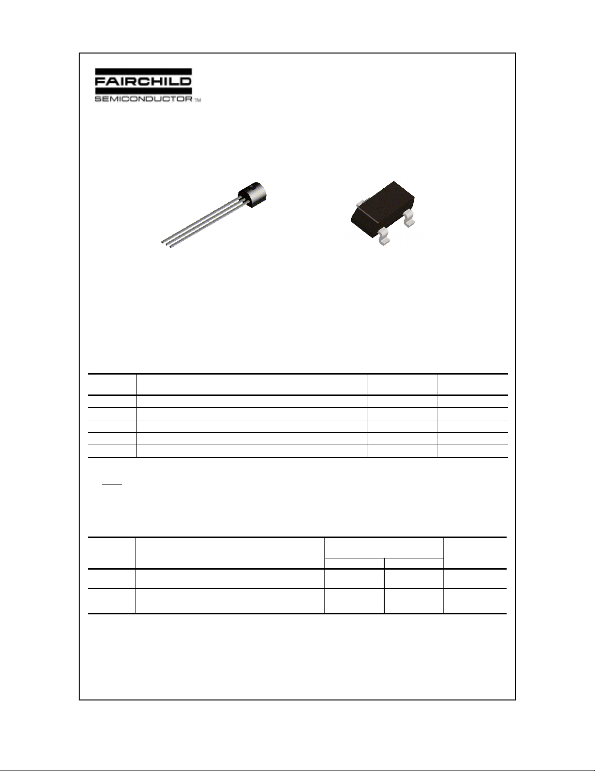
2N4126 MMBT4126
C
B
E
PNP General Purpose Amplifier
This device is designed for general purpose amplifier and switching
applications at collector currents to 10 µA as a switch and to 100
mA as an amplifier. Sourced from Process 66. See 2N3906 for
characteristics.
TO-92
C
SOT-23
Mark: ZF
2N4126 / MMBT4126
Discrete POWER & Signal
Technologies
E
B
Absolute Maximum Ratings* TA = 25°C unless otherwise noted
Symbol Parameter Value Units
V
CEO
V
CBO
V
EBO
I
C
TJ, T
stg
Collector-Emitter Voltage 25 V
Collector-Base Voltage 25 V
Em i t ter- Base Voltage 4. 0 V
Col l ector Cur re nt - Cont inuous 200 mA
Operating and Storage Junction Temperature Range -55 to +150 °C
*These ratings are limiting values above which the serviceability of any semiconductor device may be impaired.
NOTES:
1) These ratings are based on a maximum junction temperature of 150 degrees C.
2) These are steady state limits. The factory should be consulted on applications involving pulsed or low duty cycle operations.
Thermal Characteristics TA= 25°C unless otherwise noted
Symbol Characte rist i c Max Un i ts
2N4126 *MMBT4126
P
D
R
θ
JC
R
θ
JA
*Device mounted on FR-4 PCB 1.6" X 1.6" X 0.06."
Total Device Dissipation
Derate above 25°C
Thermal Resistance, Junctio n to C ase 83.3
Thermal Resistance, Junctio n to Ambien t 200 357 °C/W
625
5.0
350
2.8
mW
mW/°C
°C/W
1997 Fairchild Semiconductor Corporation
PNP General Purpose Amplifier
(continued)
Electrical Characteristics TA = 25°C unless otherwise noted
Symbol Parameter Test Conditions Min Max Units
OFF CHARACTERISTICS
V
(BR)CEO
V
(BR)CBO
V
(BR)EBO
I
CBO
I
EBO
ON CHARACTERISTICS*
h
FE
V
sat
CE(
V
sat
BE(
SMALL SIGNAL CHARACTERISTICS
f
T
C
ibo
C
cb
h
fe
NF Noise Figure
*Pulse Test: Pulse Width ≤ 300 µs, Duty Cycle ≤ 2.0%
Collector-Emitter Breakdown Voltage IC = 1.0 m A, IB = 0 25 V
Collector-Base Breakdown Voltage IC = 10 µA, IE = 0 25 V
Em i t ter- Base Break dow n V oltag e
= 10 µA, IC = 0
I
C
Collector Cutoff Current VCB = 20 V, I
= 0 50 nA
E
4.0 V
Emitter Cutoff Current VEB = 3.0 V, IC = 0 50 nA
DC Cu r re n t Gain IC = 2.0 m A, VCE = 1.0 V
I
= 50 mA, VCE = 1.0 V
Collector-Emitter Saturation Voltage IC = 50 mA, IB = 5.0 mA 0.4 V
)
Base-E m i tter Saturation Vol t ag e IC = 50 mA, IB = 5.0 mA 0.95 V
)
C
Current Gain - Bandwidth Product IC = 10 mA, VCE = 20 V,
120
60
250 MHz
f = 100 MHz
Input Capacitance VEB = 0.5 V, IC = 0,
f = 1. 0 M H z
Collector-Base Capcitance VCB = 5.0 V, IE = 0,
f = 100 kHz
Small-Signal Current Gain IC = 2.0 m A, VCE = 10 V,
120 480
f = 1. 0 kHz
= 100 µA, VCE = 5.0 V,
I
C
=1.0 kΩ, f=10 Hz to 15.7 kHz
R
S
360
10 pF
4.5 pF
4.0 dB
2N4126 / MMBT4126
 Loading...