

Fairchild Semiconductor 2N4124 Datasheet
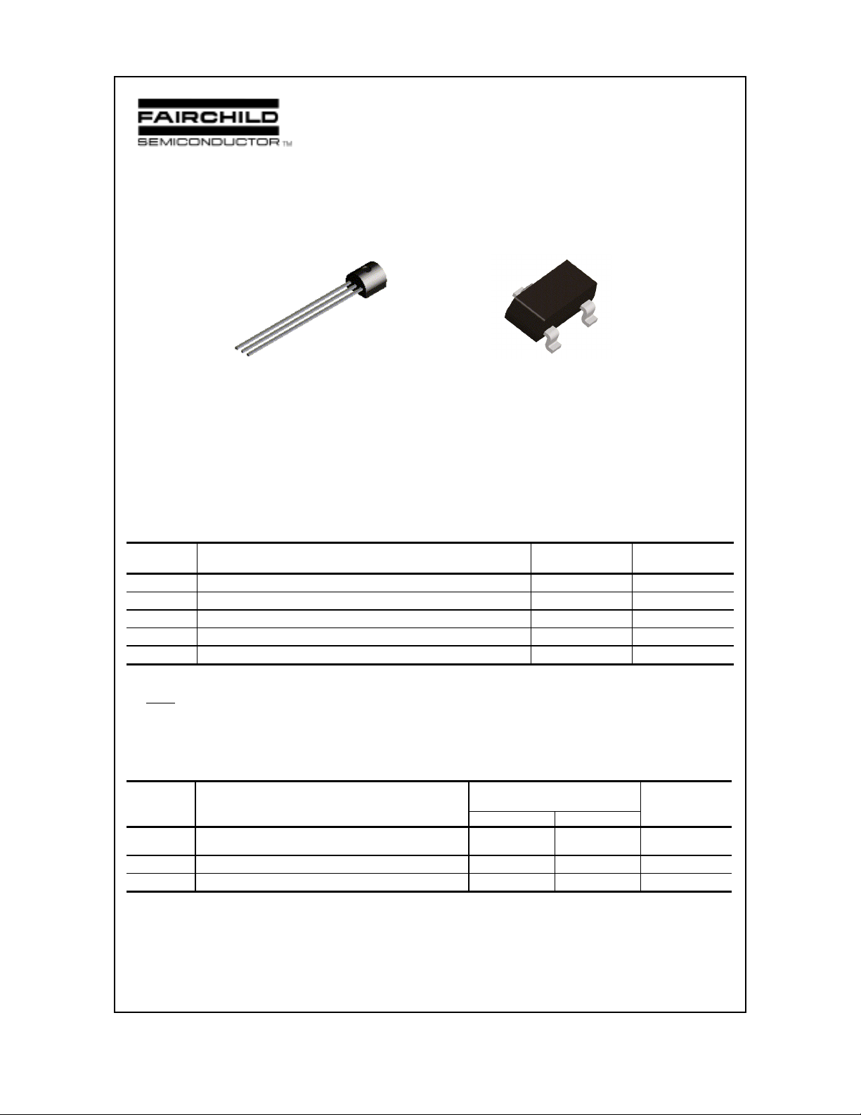
2N4124 MMBT4124
C
B
E
NPN General Purpose Amplifier
This device is designed as a general purpose amplifier and switch.
The useful dynamic range extends to 100 mA as a switch and to
100 MHz as an amplifier. Sourced from Process 23. See 2N3904
for characteristics.
TO-92
C
SOT-23
Mark: ZC
2N4124 / MMBT4124
Discrete POWER & Signal
Technologies
E
B
Absolute Maximum Ratings* TA = 25°C unless otherwise noted
Symbol Parameter Value Units
V
CEO
V
CBO
V
EBO
I
C
TJ, T
stg
Collector-Emitter Voltage 25 V
Collector-Base Voltage 30 V
Em i t ter - Bas e V olt ag e 5. 0 V
Collector Current - Continuous 200 mA
Operating and Storage Junction Temperature Range -55 to +150
°C
*These ratings are limiting values above which the serviceability of any semiconductor device may be impaired.
NOTES:
1) These ratings are based on a maximum junction temperature of 150 degrees C.
2) These are steady state limits. The factory should be consulted on applications involving pulsed or low duty cycle operations.
Thermal Characteristics TA = 25°C unless otherwise noted
Symbol Characteri st ic Max Units
2N4124 *MMBT4124
P
D
R
θ
JC
R
θ
JA
*Device mounted on FR-4 PCB 1.6" X 1.6" X 0.06."
Total De vice Dissip at i on
Derate above 25°C
Thermal Resistance, Junction to Case 83.3
Thermal Resistance, Junction to Ambient 200 357 °C/W
625
5.0
350
2.8
mW
mW/°C
°C/W
1997 Fairchild Semiconductor Corporation
NPN General Purpose Amplifier
(continued)
Electrical Characteristics TA = 25°C unless otherwise noted
Symbol Parameter Test Conditions Min Max Units
OFF CHARACTERISTICS
V
(BR)CEO
V
(BR)CBO
V
(BR)EBO
I
CBO
I
EBO
ON CHARACTERISTICS*
h
FE
V
sat
CE(
V
sat
BE(
SMALL SIGNAL CHARACTERISTICS
f
T
C
obo
C
ibo
C
cb
h
fe
NF Noise Figure
*Pulse Test: Pulse Width ≤ 300 µs, Duty Cycle ≤ 2.0%
Collector-Emitter Breakdown Voltage IC = 1.0 m A, IB = 0 25 V
C oll ec t or -Base Breakd ow n Volt age IC = 10 µA, IE = 0 30 V
Em i t ter - Bas e B r e akdown Vol tage
= 10 µA, IC = 0
I
C
Colle c tor Cu tof f Cu r ren t VCB = 20 V, I
= 0 50 nA
E
5.0 V
Emit ter Cutoff C u rre nt VEB = 3.0 V, IC = 0 50 nA
DC Cu r re n t Ga in IC = 2.0 m A, VCE = 1.0 V
I
= 50 mA, VCE = 1.0 V
Collector-Emitter Saturation Voltage IC = 50 mA, IB = 5.0 mA 0.3 V
)
Base-Emitter Saturation Voltage IC = 50 mA, IB = 5.0 mA 0.95 V
)
C
Current Gain - Bandwidth Product IC = 10 mA, VCE = 20 V,
120
60
300 MHz
f = 10 0 M Hz
Output Capacitance VCB = 5.0 V, IE = 0,
f = 10 0 kHz
Input Capacitance VBE = 0.5 V, IC = 0,
f = 1. 0 kHz
Collector-Base Capcitance VCB = 5.0 V, IE = 0,
f = 10 0 kHz
Small-Signal Current Gain VCE = 10 V, IC = 2.0 mA,
120 480
f = 1. 0 kHz
= 100 µA, VCE = 5.0 V,
I
C
=1.0kΩ, f=10 Hz to 15.7 kHz
R
S
360
4.0 pF
8.0 pF
4.0 pF
5.0 dB
2N4124 / MMBT4124
 Loading...