

Fairchild Semiconductor 2N3704 Datasheet
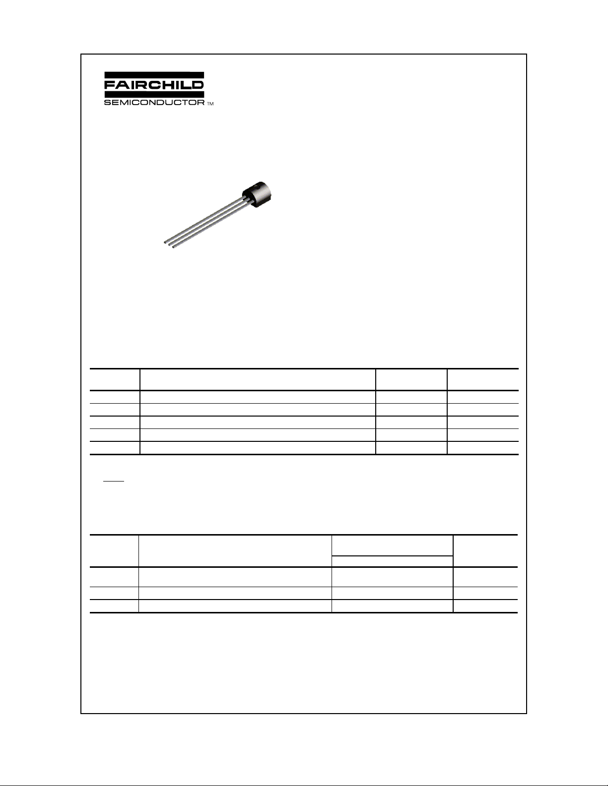
2N3704
2N3704
B
C
E
TO-92
NPN General Purpose Amplifier
This device is designed for use as general purpose amplifiers
and switches requiring collector currents to 300 mA. Sourced
from Process 10. See PN100 for characteristics.
Absolute Maximum Ratings* TA = 25°C unless otherwise noted
Symbol Parameter Value Units
V
CEO
V
CBO
V
EBO
I
C
TJ, T
stg
*These ratings are limiting values above which the serviceability of any semiconductor device may be impaired.
NOTES:
1) These ratings are based on a maximum junction temperature of 150 degrees C.
2) These are steady state limits. The factory should be consulted on applications involving pulsed or low duty cycle operations.
Thermal Characteristics TA = 25°C unless otherwise noted
Collector-Emitter Voltage 30 V
Collector-Base Voltage 50 V
Emitter-Base Voltage 5.0 V
Collector Current - Continuous 500 mA
Operating and Storage Junction Temperature Range -55 to +150
°
C
Symbol Characteristic Max Units
2N3704
P
D
R
θ
JC
R
θ
JA
1997 Fairchild Semiconductor Corporation
Total Device Dissipa tion
Derate above 25°C
Ther mal Resistance, Junction to Case 83.3
Thermal Resistan ce, Junction to Ambient 200
625
5.0
mW
mW/°C
C/W
°
C/W
°
NPN General Purpose Amplifier
(continued)
Electrical Characteristics TA = 25°C unless otherwise noted
Symbol Parameter Test Conditions Min Max Units
OFF CHARACTERISTICS
V
(BR)CEO
V
(BR)CBO
V
(BR)EBO
I
CBO
I
EBO
ON CHARACTERISTICS*
h
FE
V
(on)
BE
V
(sat)
CE
SMALL SIGNAL CHARACTERISTICS
C
ob
f
T
*Pulse Test: Pulse Width ≤ 300 µs, Duty Cycle ≤ 2.0%
Collector-Emitte r Breakdown Voltage* IC = 10 mA, IB = 030V
Collector-Base Breakdown Voltag e
Emitter-Base Breakdown Voltage
I
= 100 µA, IE = 0
C
I
= 100 µA, IC = 0
E
50 V
5.0 V
Collector Cutoff Current VCB = 20 V, IE = 0 100 nA
Emitter Cutoff Current VEB = 3.0 V, IC = 0 100 nA
DC Current Gain VCE = 2.0 V, IC = 50 mA 100 300
Base-Emitter ON Volta ge VCE = 2.0 V, IC = 100 mA 0.5 1.0 V
Collector-Emitte r Saturation Voltage IC = 100 mA, IB = 5.0 mA 0.6 V
Output Capacitance VCB = 10 V, f = 1.0 MHz 12 pF
Current Gain - Bandwidth Product IC = 50 mA, VCE = 2.0 V, 100 MHz
2N3704
 Loading...