Fairchild Semiconductor 100311QIX, 100311QI, 100311QCX, 100311QC, 100311CW Datasheet

© 1999 Fairchild Semiconductor Corporation DS010648 www.fairchildsemi.com
February 1990
Revised November 1999
100311 Low Skew 1:9 Differential Clock Driver
100311
Low Skew 1:9 Differential Clock Driver
General Description
The 100311 contains nine low skew differential drivers,
designed for genera tion of multiple, mini mum skew differential clocks from a single differential input (CLKIN,
CLKIN
). If a single-ende d input is desir ed, the VBB output
pin may be used to driv e the rema ining inpu t line. A HIGH
on the enable pin (EN
) will force a LOW on all of the CLK
n
outputs and a HIGH on all of the CLKn output pins. The
100311 is ideal for distributing a signal throughout a system
without worrying about the original signal becoming too
corrupted by undesirable delays and skew.
Features
■ Low output-to-output skew
■ 2000V ESD protection
■ 1:9 low skew clock driver
■ Differential inputs and outputs
■ Available to industrial grade temperature range
(PLCC package only)
Ordering Code:
Devices also availab le in Tape and Reel. Specify by appending th e s uffix let t er “X” to the ordering code.
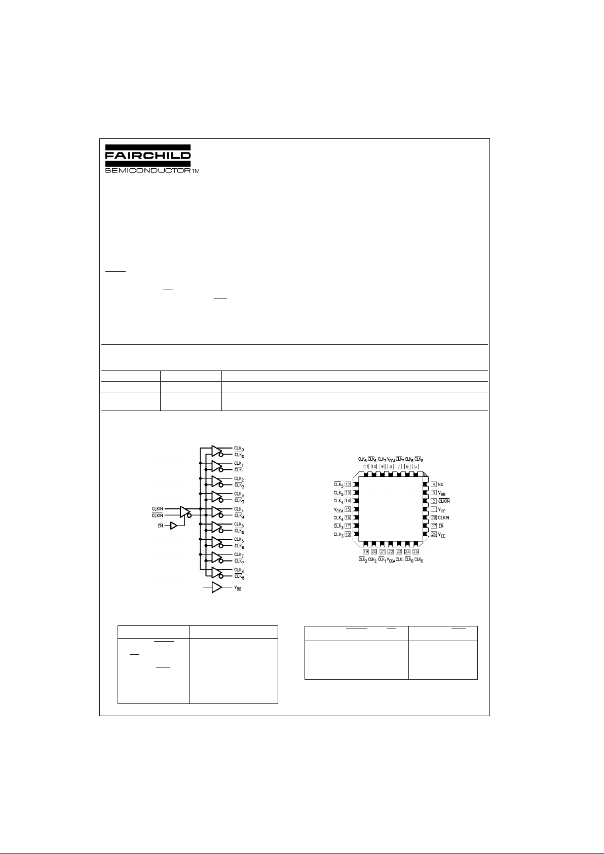
Logic Symbol
Pin Descriptions
Connection Diagram
28-Pin PLCC
Truth T able
Order Number Package Number Package Description
100311QC V28A 28-Lead Plastic Lead Chip Carrier (PLCC), JEDEC MO-047, 0.450 Square
100311QI V28A 28-Lead Plastic Lead Chip Carrier (PLCC), JEDEC MO-047, 0.450 Square
Industrial Temperature Range (−40°C to +85°C)
Pin Names Description
CLKIN, CLKIN
Differential Clock Inputs
EN
Enable
CLK
0–8
, CLK
0–8
Differential Clock Outputs
V
BB
VBB Output
NC No Connect
CLKIN CLKIN EN CLK
n
CLK
n
LHLLH
HLLHL
XXHLH

www.fairchildsemi.com 2
100311
Absolute Maximum Ratings(Note 1) Recommended Operating
Conditions
Note 1: The “Absolute Maximum Ratings” are those values beyon d which
the safety of the dev ice cannot be guaranteed. T he device sh ould not be
operated at these limit s. The parametric values defin ed in the Electrical
Characteristics tables are not guaranteed at the absolute maximum rating.
The “Recomme nded O peratin g Cond itions ” table will defin e the condition s
for actual device operation.
Note 2: ESD testing conf orm s t o M I L-STD-883, Method 3015.
Commercial Version
DC Electrical Characteristics
(Note 3)
V
EE
= −4.2V to −5.7V, VCC = V
CCA
= GND, TC = 0°C to +85°C
Note 3: The specified limits represent the “worst case” value for the parameter. Since these values normally occur at the temperature extremes, additional
noise immunity and guardbanding can be achieved by decreasing the all owable syste m opera ti ng r ange s. Co ndi ti ons fo r t est ing shown in the ta ble s are chosen to guarantee operation under “worst case” conditions.
Storage Temperature (T
STG
) −65°C to +150°C
Maximum Junction Temperature (T
J
) +150°C
Pin Potential to Ground Pin (V
EE
) −7.0V to +0.5V
Input Voltage (DC) V
EE
to +0.5V
Output Current (DC Output HIGH) −50 mA
ESD (Note 2) ≥2000V
Case Temperature (T
C
)
Commercial 0°C to +85°C
Industrial −40°C to +85°C
Supply Voltage ( V
EE
) −5.7V to −4.2V
Symbol Parameter Min Typ Max Units Conditions
V
OH
Output HIGH Voltage −1025 −955 −870 mV VIN = VIH (Max) Loading with
V
OL
Output LOW Voltage −1830 −1705 −1620 mV or VIL (Min) 50Ω to −2.0V
V
OHC
Output HIGH Voltage −1035 mV VIN = VIH Loading with
V
OLC
Output LOW Voltage −1610 mV or VIL (Max) 50Ω to −2.0V
V
BB
Output Reference Voltage −1380 −1320 −1260 mV I
VBB
= −300 µA
V
DIFF
Input Voltage Differential 150 mV Required for Full Output Swing
V
CM
Common Mode Voltage VCC − 2.0 VCC − 0.5 V
V
IH
Input HIGH Voltage −1165 −870 mV Guaranteed HIGH Signal for
All Inputs
V
IL
Input LOW Voltage −1830 −1475 mV Guaranteed LOW Signal for
All Inputs
I
IL
Input LOW Current 0.50 µAVIN = VIL (Min)
I
IH
Input HIGH Current VIN = VIH (Max)
CLKIN, CLKIN 100 µA
EN
250
I
CBO
Input Leakage Current −10 µAVIN = V
EE
I
EE
Power Supply Current −115 −57 mA Inputs Open
 Loading...