


April 2010
FSBH0F70A, FSBH0170/A, FSBH0270/A, FSBH0370
Green Mode Fairchild Power Switch (FPS™)
FSBH0F70A, FSBH0170/A, FSBH0270/A, FSBH0370 — Green Mode Fairchild Power Switch (FPS™)
Features
Brownout Protection with Hysteresis
Built-In 5ms Soft-Start Function
Internal Avalanche-Rugged 700V SenseFET
No Acoustic Noise During Light-Load Operation
High-Voltage Startup
Linearly Decreasing PWM Frequency to 18KHz
Peak-Current-Mode Control
Cycle-by-Cycle Current Limiting
Leading-Edge Blanking (LEB)
Synchronized Slope Compensation
Internal Open-Loop Protection
V
V
Under-Voltage Lockout (UVLO)
DD
Over-Voltage Protection (OVP)
DD
Internal Auto-Restart Circuit (OVP, OTP)
Constant Power Limit (Full AC Input Range)
Internal OTP Sensor with Hysteresis
VIN Pin for Pull-HIGH Latch Function and Pull-
LOW Auto-Recovery Protection
Applications
General-purpose switch-mode power supplies and
flyback power converters, including:
Auxiliary Power Supply for PC and Server
SMPS for VCR, SVR, STB, DVD & DVCD Player,
Printer, Facsimile, and Scanner
Adapter for Camcorder
Description
The highly integrated FSBH-series consists of an
integrated current-mode Pulse Width Modulator (PWM)
and an avalanche-rugged 700V SenseFET. It is
specifically designed for high-performance offline
Switch Mode Power Supplies (SMPS) with minimal
external components.
The integrated PWM controller features include a
proprietary green-mode function that provides off-time
modulation to linearly decrease the switching frequency
at light-load conditions to minimize standby power
consumption. To avoid acoustic-noise problems, the
minimum PWM frequency is set above 18kHz. This
green-mode function enables the power supply to meet
international power conservation requirements. The
PWM controller is manufactured using the BiCMOS
process to further reduce power consumption. The
FSBH-series turns off some internal circuits to improve
power saving when V
an operating current of only 2.5mA.
The FSBH-series has built-in synchronized slope
compensation to achieve stable peak-current-mode
control. The proprietary external line compensation
ensures constant output power limit over a wide AC
input voltage range, from 90V
The FSBH-series provides many protection functions. In
addition to cycle-by-cycle current limiting, the internal
open-loop protection circuit ensures safety when an
open-loop or output short occurs. PWM output is
disabled until V
controller starts up again. As long as V
the internal OVP circuit is triggered.
Compared with a discrete MOSFET and controller or
RCC switching converter solution, the FSBH-series
reduces total component count, design size, and
weight; while increasing efficiency, productivity, and
system reliability. These devices provide a basic
platform that is well suited for the design of costeffective flyback converters, such as in PC auxiliary
power supplies.
is lower than 1.6V, which allows
FB
to 264VAC.
AC
drops below the V
DD
TH-OLP
DD
, then the
exceeds 28V,
© 2009 Fairchild Semiconductor Corporation www.fairchildsemi.com
FSBH0F70A, FSBH0170/A, FSBH0270/A, FSBH0370 • Rev. 1.0.3
Ordering Information
FSBH0F70A, FSBH0170/A, FSBH0270/A, FSBH0370 — Green Mode Fairchild Power Switch (FPS™)
Part Number Sense FET
Operating
Temperature Range
FSBH0F70ANY 0.5A 700V -40°C to +105°C
FSBH0170ANY 1.0A 700V -40°C to +105°C
FSBH0270ANY 2.0A 700V -40°C to +105°C
FSBH0170NY 1.0A 700V -40°C to +105°C
FSBH0370NY 3.0A 700V -40°C to +105°C
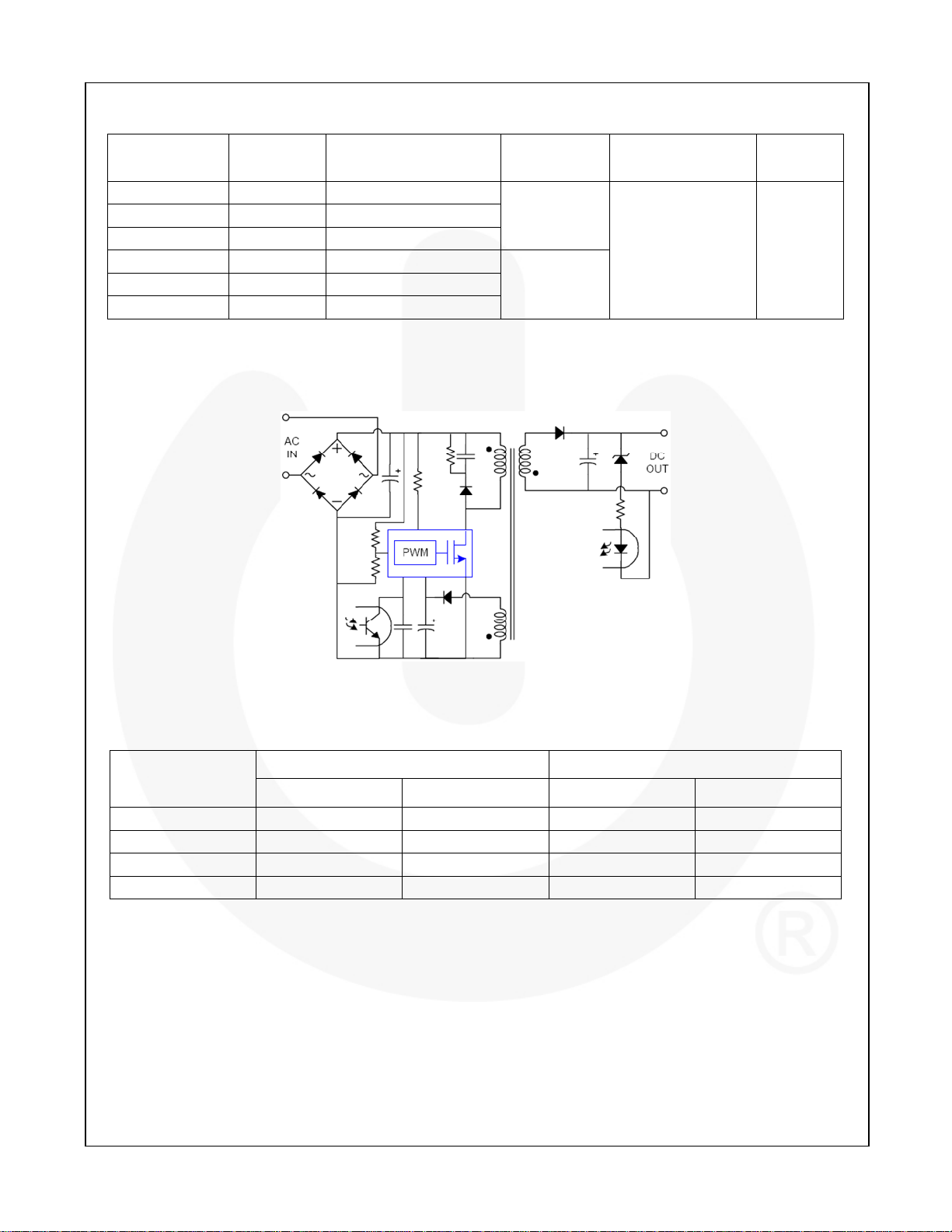
Application Diagram
HV
Drain
VIN
GNDVDDFB
VIN Pin
(PIN #4)
Not Available
Enabled FSBH0270NY 2.0A 700V -40°C to +105°C
Package
8-Pin Dual In-Line
Package (DIP)
Packing
Method
Tube
Figure 1. Typical Flyback Application
Output Power Table
Product
FSBH0F70A 7W 10W 6W 8W
FSBH0170/A 10W 15W 9W 13W
FSBH0270/A 14W 20W 11W 16W
FSBH0370 17.5W 25W 13W 19W
Notes:
1. The maximum output power can be limited by junction temperature.
2. 230 V
3. Typical continuous power in a non-ventilated enclosed adapter with sufficient drain pattern as a heat sink at
50°C ambient.
4. Maximum practical continuous power in an open-frame design with sufficient drain pattern as a heat sink at
50°C ambient.
or 100/115 V
AC
(1)
Adapter
with doublers.
AC
230V
± 15%
AC
(3)
Open Frame
(2)
85-265VAC
(4)
Adapter
(3)
Open Frame
(4)
© 2009 Fairchild Semiconductor Corporation www.fairchildsemi.com
FSBH0F70A, FSBH0170/A, FSBH0270/A, FSBH0370 • Rev. 1.0.3 2
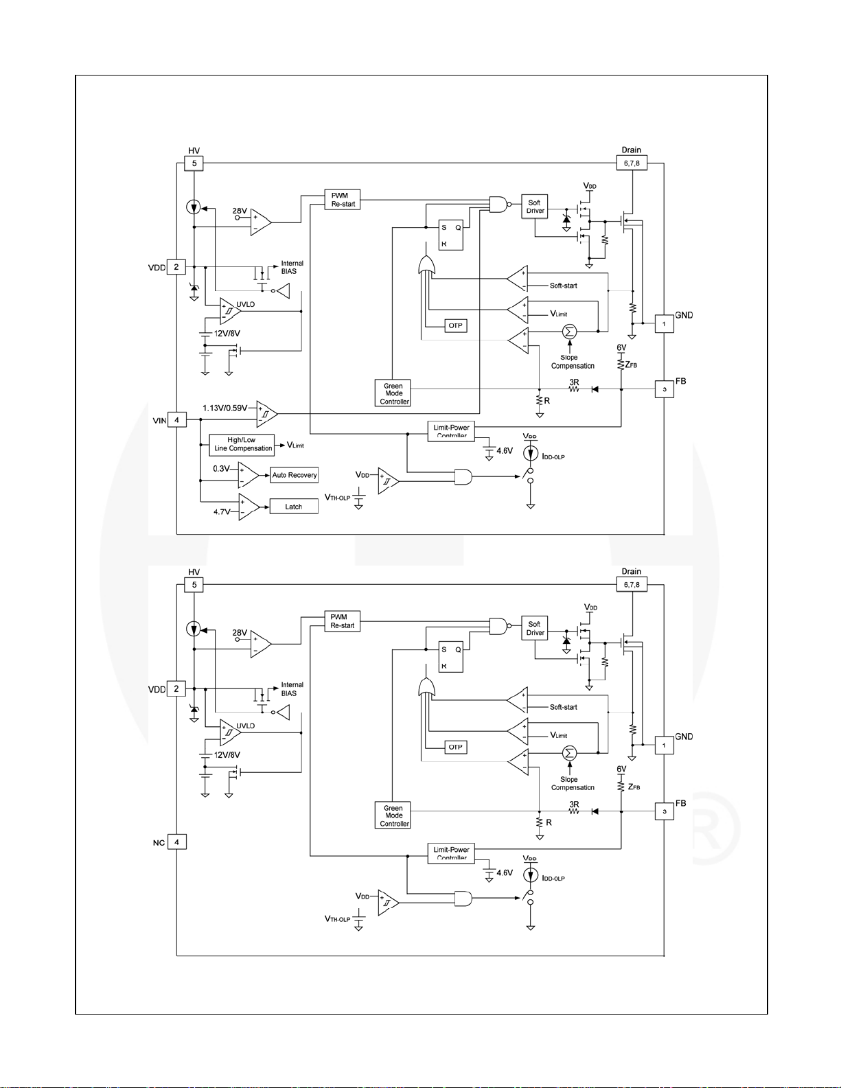
Internal Block Diagrams
FSBH0F70A, FSBH0170/A, FSBH0270/A, FSBH0370 Green — Mode Fairchild Power Switch (FPS™)
Figure 2. FSBH0170, FSBH0270, FSBH0370 Internal Block Diagram
Figure 3. FSBH0F70A, FSBH0170A, FSBH0270A Internal Block Diagram
© 2009 Fairchild Semiconductor Corporation www.fairchildsemi.com
FSBH0F70A, FSBH0170/A, FSBH0270/A, FSBH0370 • Rev. 1.0.3 3
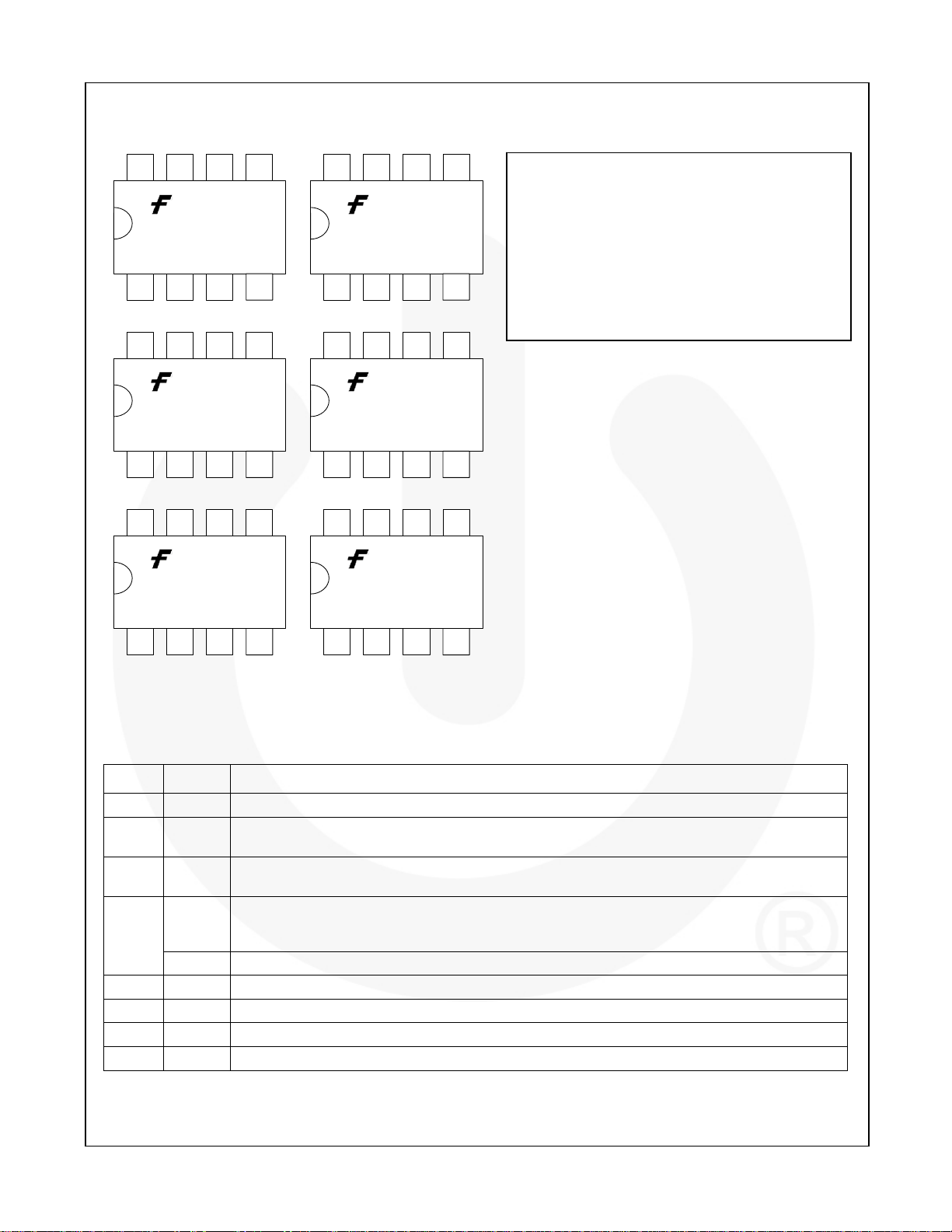
Pin Configuration
FSBH0F70A, FSBH0170/A, FSBH0270/A, FSBH0370 — Green Mode Fairchild Power Switch (FPS™)
8
ZXYTT
BH0F70A
TPM
1
8
ZXYTT
BH0270A
TPM
1
8
ZXYTT
BH0270
TPM
8
ZXYTT
BH0170A
TPM
1
8
ZXYTT
BH0170
TPM
1
8
ZXYTT
BH0370
TPM
F – Fairchild Logo
Z – Plant Code
X – 1-Digit Year Code
Y – 1-Digit Week Code
TT – 2-Digit Die Run Code
T – Package Type (N:DIP)
P – Y: Green Package
M – Manufacture Flow Code
1
Figure 4. Pin Configuration and Top Mark Information
Pin Definitions
Pin # Name Description
1 GND
2 VDD
3 FB
4
5 HV
6 Drain
7 Drain
8 Drain
VIN
NC No Connection for FSBH0F70A, FSBH0170A and FSBH0270A.
Ground. SenseFET source terminal on primary side and internal controller ground.
Power Supply. The internal protection circuit disables PWM output as long as V
OVP trigger point.
Feedback. The signal from the external compensation circuit is fed into this pin. The PWM duty
cycle is determined in response to the signal on this pin and the internal current-sense signal.
Line-Voltage Detection. The line-voltage detection is used for brownout protection with
hysteresis and constant output power limit over universal AC input range. This pin has additional
protections that are pull-HIGH latch and pull-LOW auto recovery, depending on the application.
Startup. For startup, this pin is pulled HIGH to the line input or bulk capacitor via resistors.
SenseFET Drain. High-voltage power SenseFET drain connection.
SenseFET Drain. High-voltage power SenseFET drain connection.
SenseFET Drain. High-voltage power SenseFET drain connection.
1
exceeds the
DD
© 2009 Fairchild Semiconductor Corporation www.fairchildsemi.com
FSBH0F70A, FSBH0170/A, FSBH0270/A, FSBH0370 • Rev. 1.0.3 4
Absolute Maximum Ratings
Stresses exceeding the absolute maximum ratings may damage the device. The device may not function or be
operable above the recommended operating conditions and stressing the parts to these levels is not recommended.
In addition, extended exposure to stresses above the recommended operating conditions may affect device
reliability. The absolute maximum ratings are stress ratings only.
Symbol Parameter Min. Max. Unit
V
Drain Pin Voltage
DRAIN
IDM Drain Current Pulsed
EAS Single Pulsed Avalanche Energy
VDD DC Supply Voltage 30 V
VFB FB Pin Input Voltage -0.3 7.0 V
VIN VIN Pin Input Voltage -0.3 7.0 V
VHV HV Pin Input Voltage 700 V
P
Power Dissipation (T
D
θJA Junction-to-Air Thermal Resistance 80
θJC Junction-to-Case Thermal Resistance 20
TJ Operating Junction Temperature Internally limited
T
Storage Temperature Range -55 +150
STG
TL Lead Temperature (Wave Soldering or IR, 10 Seconds) +260
ESD
Electrostatic Discharge Capability,
All pins except HV pin
Notes:
5. All voltage values, except differential voltages, are given with respect to the network ground terminal.
6. Stresses beyond those listed under Absolute Maximum Ratings may cause permanent damage to the device.
7. Non-repetitive rating: pulse width is limited by maximum junction temperature.
8. L = 51mH, starting T
9. Internally Limited of T
(5,6)
FSBH0x70/A 700 V
FSBH0F70A 1.5
(7)
FSBH0170/A 4.0
FSBH0270/A 8.0
A
FSBH0370 12.0
FSBH0F70A 10
(8)
FSBH0170/A 50
FSBH0270/A 140
mJ
FSBH0370 230
<50°C) 1.5 W
A
°C/W
°C/W
(9)
°C
°C
°C
= 25°C.
J
refers to T
J
OTP
Human Body Model:
JESD22-A114
Charged Device Model:
JESD22-C101
3
kV
1
FSBH0F70A, FSBH0170/A, FSBH0270/A, FSBH0370 — Green Mode Fairchild Power Switch (FPS™)
Recommended Operating Conditions
The Recommended Operating Conditions table defines the conditions for actual device operation. Recommended
operating conditions are specified to ensure optimal performance to the datasheet specifications. Fairchild does not
recommend exceeding them or designing to Absolute Maximum Ratings.
Symbol Parameter Conditions Min. Typ. Max. Unit
TA Operating Ambient Temperature -40 +105 °C
© 2009 Fairchild Semiconductor Corporation www.fairchildsemi.com
FSBH0F70A, FSBH0170/A, FSBH0270/A, FSBH0370 • Rev. 1.0.3 5

FSBH0F70A, FSBH0170/A, FSBH0270/A, FSBH0370 — Green Mode Fairchild Power Switch (FPS™)
Electrical Characteristics
VDD=15V and TA=25°C unless otherwise specified.
Symbol Parameter Condition Min. Typ. Max. Unit
SenseFET Section
BV
DSS
I
DSS
R
DS(ON)
C
Input Capacitance
ISS
C
Output Capacitance
OSS
C
RSS
t
Turn-On Delay Time
D(ON)
tR Rise Time
t
Turn-Off Delay Time
D(OFF)
tF Fall Time
(10)
Drain-Source
Breakdown Voltage
Zero-Gate-Voltage
Drain Current
Drain-Source OnState Resistance
(11)
Reverse Transfer
Capacitance
FSBH0x70/A VDS = 700V, VGS = 0V 700 V
V
= 700V, VGS = 0V 50
DS
FSBH0x70/A
FSBH0F70A
FSBH0170/A 8.80 11.00
FSBH0270/A 6.00 7.20
VDS = 560V, VGS = 0V,
T
= 125°C
C
V
= 10V, ID = 0.5A
GS
200
14.00 19.00
μA
Ω
FSBH0370 4.00 4.75
FSBH0F70A
FSBH0170/A 250 325
FSBH0270/A 550 715
VGS = 0V, VDS = 25V,
f = 1MHz
162 211
pF
FSBH0370 315 410
FSBH0F70A
FSBH0170/A 25 33
FSBH0270/A 38 50
VGS = 0V, VDS = 25V,
f = 1MHz
18 24
pF
FSBH0370 47 61
FSBH0F70A
FSBH0170/A 10.0 15.0
FSBH0270/A 17.0 26.0
V
= 0V, VDS = 25V,
GS
f = 1MHz
3.8 5.7
pF
FSBH0370 9.0 24.0
FSBH0F70A
FSBH0170/A 12.0 34.0
FSBH0270/A 20.0 50.0
VDS = 350V, ID = 1.0A
9.5 29.0
ns
FSBH0370 11.2 33.0
FSBH0F70A
FSBH0170/A 4 18
FSBH0270/A 15 40
VDS = 350V, ID = 1.0A
19 48
ns
FSBH0370 34 78
FSBH0F70A
FSBH0170/A 30.0 70.0
FSBH0270/A 55.0 120.0
VDS = 350V, ID = 1.0A
33.0 76.0
ns
FSBH0370 28.2 67.0
FSBH0F70A
FSBH0170/A 10 30
FSBH0270/A 25 60
VDS = 350V, ID = 1.0A
42 94
ns
FSBH0370 32 74
Continued on the following page…
© 2009 Fairchild Semiconductor Corporation www.fairchildsemi.com
FSBH0F70A, FSBH0170/A, FSBH0270/A, FSBH0370 • Rev. 1.0.3 6

FSBH0F70A, FSBH0170/A, FSBH0270/A, FSBH0370 — Green Mode Fairchild Power Switch (FPS™)
Electrical Characteristics (Continued)
VDD=15V and TA=25°C unless otherwise specified.
Symbol Parameter Condition Min. Typ. Max. Unit
Control Section
VDD Section
V
Start Threshold Voltage 11 12 13 V
DD-ON
V
Minimum Operating Voltage 7 8 9 V
DD-OFF
FSBH0170
I
Startup Current
DD-ST
I
Operating Supply Current VDD = 15V, VFB = 3V 3.0 3.5 4.0 mA
DD-OP
I
Operating Current for VFB<V
DD-ZDC
I
Internal Sink Current
DD-OLP
V
I
TH-OLP
V
VDD Over-Voltage Protection 27 28 29 V
DD-OVP
t
D-VDD-OVP
HV Section
FSBH0270
FSBH0370
FSBH0F70A
FSBH0170A
FSBH0270A
FB-ZDC
Off Voltage 5 6 7 V
DD-OLP
VDD Over-Voltage Protection
Debounce Time
V
– 0.16V 30
DD-ON
µA
V
– 0.16V 240 320 400
DD-ON
VDD = 12V, VFB = 1.6V 1.5 2.5 3.5 mA
V
TH-OLP
+0.1V
30 70 90 µA
75 130 200 µs
IHV Maximum Current Drawn from HV Pin
I
Leakage Current after Startup
HV-LC
HV 120VDC,
V
= 0V with 10µF
DD
HV = 700V,
V
= V
DD
DD-OFF
+1V
1.5 3.5
5.0 mA
1 20 µA
Oscillator Section
f
Frequency in Nominal Mode
OSC
f
Green-Mode Frequency 14 18 22 kHz
OSC-G
D
Maximum Duty Cycle 85 %
MAX
Center Frequency
94 100 106 kHz
fDV Frequency Variation vs. VDD Deviation VDD = 11V to 22V 5 %
fDT
Frequency Variation vs. Temperature
Deviation
(10)
= -25 to 85°C
T
A
5 %
VIN Section (FSBH0170, FSBH0270, FSBH0370)
V
PWM Turn-On Threshold Voltage
IN-ON
V
PWM Turn-Off Threshold Voltage
IN-OFF
t
PWM Turn-Off Debounce Time
IN-OFF
V
Pull-HIGH Latch Trigger Level
IN-H
t
Pull-HIGH Latch Debounce Time
IN-H
V
IN-L
Pull-LOW Auto-Recovery Trigger
Level
1.08 1.13 1.18 V
V
–
V
–
IN-ON
0.48
IN-ON
0.54
V
IN-ON
0.60
500
4.4 4.7 5.0
100
0.2 0.3 0.4
Feedback Input Section
AV
FB Voltage to Current-Sense
Attenuation
1/4.5 1/4.0 1/3.5 V/V
ZFB Input Impedance 4 7 kΩ
–
V
ms
V
µs
V
Continued on the following page…
© 2009 Fairchild Semiconductor Corporation www.fairchildsemi.com
FSBH0F70A, FSBH0170/A, FSBH0270/A, FSBH0370 • Rev. 1.0.3 7

FSBH0F70A, FSBH0170/A, FSBH0270/A, FSBH0370 — Green Mode Fairchild Power Switch (FPS™)
Electrical Characteristics (Continued)
VDD=15V and TA=25°C unless otherwise specified.
Symbol Parameter Condition Min. Typ. Max. Unit
V
V
V
Current-Sense Section
Constant Power Limit (FSBH0170, FSBH0270, FSBH0370)
Current Limit (FSBH0F70A, FSBH0170A, FSBH0270A)
Over-Temperature Protection Section (OTP)
T
Notes:
10. These parameters, although guaranteed, are not 100% tested in production.
11. Pulse test: pulse width ≤ 300ìs, duty ≤ 2%.
12. When activated, the output is disabled and the latch is turned off.
13. The threshold temperature for enabling the output again and resetting the latch after over-temperature
14. These parameters, although guaranteed, are tested in wafer process.
Output High Voltage FB Pin Open 5.5 V
FB-OPEN
V
Green-Mode Entry FB Voltage 2.3 2.5 2.7 V
FB-N
V
Green-Mode Ending FB Voltage 1.9 2.0 2.1 V
FB-G
Zero Duty Cycle FB Voltage
FB-ZDC
FB-OLP
t
D-OLP
Trigger Level
FB Open-Loop Protection Delay 50 56 59 ms
(14)
FB Open-Loop
FSBH0F70A 5.2 5.4 5.6 V
FSBH0x70/A 4.4 4.6 4.8 V
FSBH0F70A V
I
Peak Current Limit
LIM
FSBH0170/A VIN = 1.2V / VIN Open 0.70 0.80 0.90
FSBH0270/A VIN = 1.2V / VIN Open 0.90 1.00 1.10
Open 0.63 0.73 0.83
IN
1.6
FSBH0370 VIN = 1.2V 1.10 1.20 1.30
tSS Period During Soft-Start Time
V
Threshold Voltage 1 for Current Limit
LMT1
V
LMT2
V
LMT
T
OTP
RESTART
Threshold Voltage 2 for Current Limit VIN = 3.6V 0.56 0.63 0.70 V
Threshold Voltage for Current Limit
Protection Junction Temperature
Restart Junction Temperature
(10)
4.5 5.0 5.5 ms
VIN = 1.2V 0.73 0.80 0.87 V
FSBH0F70A 0.97 1.00 1.03 V
FSBH0170A/0270A
(10, 12)
+135 +142 +150 °C
(10, 13)
T
0.77 0.80 0.83 V
-25 °C
OTP
protection has been activated.
PWM Frequency
f
OSC
f
OSC-G
V
FB-ZDC
V
FB-G
V
FB-N
V
FB
V
A
Figure 5. V
vs. PWM Frequency
FB
© 2009 Fairchild Semiconductor Corporation www.fairchildsemi.com
FSBH0F70A, FSBH0170/A, FSBH0270/A, FSBH0370 • Rev. 1.0.3 8

Typical Characteristics (Continued)
FSBH0F70A, FSBH0170/A, FSBH0270/A, FSBH0370 Green — Mode Fairchild Power Switch (FPS™)
14
12
10
8
(µA )
6
DD-ST
I
4
2
0
-40 -25 -10 5 20 35 50 65 80 95 110 125
Temperature(°C)
Figure 6. I
12.4
12.2
12.0
(V)
11.8
DD-ON
V
11.6
11.4
11.2
-40 -25 -10 5 20 35 50 65 80 95 110 125
Figure 8. V
vs. Temperature Figure 7. I
DD-ST
Temperature(°C)
vs. Temperature Figure 9. V
DD-ON
3.02
3.00
2.98
2.96
(µA )
2.94
DD-OP
2.92
I
2.90
2.88
2.86
-40 -25 -10 5 20 35 50 65 80 95 110 125
Temperature(°C)
vs. Temperature
DD-OP
8.3
8.2
8.1
(V)
8.0
DD-OFF
V
7.9
7.8
7.7
-40 -25 -10 5 20 35 50 65 80 95 110 125
Temperature(°C)
vs. Temperature
DD-OFF
6.6
6.4
6.2
6.0
(V)
5.8
TH-OLP
5.6
V
5.4
5.2
5.0
-40 -25 -10 5 20 35 50 65 80 95 110 125
Temperature(°C)
(V)
DD-OVP
V
28.42
28.41
28.40
28.39
28.38
28.37
28.36
28.35
Figure 10. V
4.0
3.5
3.0
2.5
(mA)
HV
I
2.0
1.5
1.0
-40 -25 -10 5 20 35 50 65 80 95 110 125
vs. Temperature Figure 11. V
TH-OLP
7
6
5
4
(µA)
3
HV-LC
I
2
1
0
Temperature(°C)
Figure 12. IHV vs. Temperature Figure 13. I
-40 -25 -10 5 20 35 50 65 80 95 110 125
Temperature(°C)
vs. Temperature
DD-OVP
-40 -25 -10 5 20 35 50 65 80 95 110 125
Temperature(°C)
vs. Temperature
HV-LC
© 2009 Fairchild Semiconductor Corporation www.fairchildsemi.com
FSBH0F70A, FSBH0170/A, FSBH0270/A, FSBH0370 • Rev. 1.0.3 9

Typical Characteristics (Continued)
FSBH0F70A, FSBH0170/A, FSBH0270/A, FSBH0370 — Green Mode Fairchild Power Switch (FPS™)
101.5
101.0
100.5
100.0
(kHz)
99.5
OSC
99.0
F
98.5
98.0
97.5
-40 -25 -10 5 20 35 50 65 80 95 110 125
Temperature(°C)
Figure 14. f
0.64
0.63
0.62
(V)
0.61
IN-OFF
V
0.60
0.59
0.58
-40 -25 -10 5 20 35 50 65 80 95 110 125
Figure 16. V
vs. Temperature Figure 15. f
OSC
Temperature(°C)
vs. Temperature Figure 17. V
IN-OFF
19.2
19.1
19.0
(kHz )
18.9
OSC-G
F
18.8
18.7
18.6
-40 -25 -10 5 20 35 50 65 80 95 11 0 125
Temperature(°C)
vs. Temperature
OSC-G
1.17
1.16
1.15
(V)
1.14
IN-ON
V
1.13
1.12
1.11
-40 -25 -10 5 20 35 50 65 80 95 110 125
Temperature(°C)
vs. Temperature
IN-ON
4.63
4.62
4.61
(V)
4.60
IN-H
V
4.59
4.58
4.57
-40 -25 -10 5 20 35 50 65 80 95 110 125
Temperature(°C)
Figure 18. V
4.75
4.70
4.65
4.60
(V)
4.55
FB-OLP
4.50
V
4.45
4.40
4.35
-40 -25 -10 5 20 35 50 65 80 95 110 125
Figure 20. V
vs. Temperature Figure 19. V
IN-H
Temperature(°C)
vs. Temperature Figure 21. V
FB-OLP
0.34
0.33
0.32
(V)
0.31
IN-L
V
0.30
0.29
0.28
-40 -25 -10 5 20 35 50 65 80 95 110 125
2.60
2.55
2.50
(V)
2.45
FB-N
V
2.40
2.35
2.30
-40 -25 -10 5 20 35 50 65 80 95 110 125
Temperature(°C)
vs. Temperature
IN-L
Temperature(°C)
vs. Temperature
FB-N
© 2009 Fairchild Semiconductor Corporation www.fairchildsemi.com
FSBH0F70A, FSBH0170/A, FSBH0270/A, FSBH0370 • Rev. 1.0.3 10

Typical Characteristics (Continued)
FSBH0F70A, FSBH0170/A, FSBH0270/A, FSBH0370 — Green Mode Fairchild Power Switch (FPS™)
2.20
2.15
2.10
2.05
(V)
2.00
FB-G
V
1.95
1.90
1.85
1.80
-40 -25 -10 5 20 35 50 65 80 95 110 125
Temperature(°C)
Figure 22. V
2.56
2.54
2.52
2.50
(mA)
2.48
DD-ZDC
I
2.46
2.44
2.42
-40 -25 -10 5 20 35 50 65 80 95 110 125
Figure 24. I
vs. Temperature Figure 23. V
FB-G
Temperature(°C)
vs. Temperature Figure 25. t
DD-ZDC
1.800
1.700
1.600
(V)
1.500
FB-ZDC
V
1.400
1.300
1.200
-40 -25 -10 5 20 35 50 65 80 95 110 125
55.0
54.5
54.0
53.5
(ms )
53.0
D-OLP
t
52.5
52.0
51.5
-40 -25 -10 5 20 35 50 65 80 95 110 125
Temperature(°C)
vs. Temperature
FB-ZDC
Temperature(°C)
vs. Temperature
D-OLP
© 2009 Fairchild Semiconductor Corporation www.fairchildsemi.com
FSBH0F70A, FSBH0170/A, FSBH0270/A, FSBH0370 • Rev. 1.0.3 11

Functional Description
A
FSBH0F70A, FSBH0170/A, FSBH0270/A, FSBH0370 — Green Mode Fairchild Power Switch (FPS™)
Startup Operation
The HV pin is connected to bulk voltage through an
external resistor, R
, as shown in Figure 26. When AC
HV
voltage is applied to power system, an internal HV
startup circuit provides a high current (around 3.5mA) to
charge an external V
exceeds the turn-on threshold voltage (V
capacitor until VDD voltage
DD
DD-ON
). For
better power consumption, the HV startup circuit shuts
down during normal operation. The external V
capacitor and auxiliary winding maintain the V
voltage
DD
DD
and provide operating current to controller.
Figure 26. Startup Circuit
Slope Compensation
The FSBH-series is designed for flyback power
converters. The peak-current-mode control is used to
optimize system performance. Slope compensation is
added to reduce current loop gain and improve power
system stability. The FSBH-series has a built-in,
synchronized, positive slope for each switching cycle.
Brown-In/Out Funct i on
FSBH0x70 has a built-in internal brown-in/out protection
comparator monitoring voltage of VIN pin. Figure 28
shows a resistive divider with low-pass filtering for linevoltage detection on the VIN pin.
Figure 28. Brown-In/Out Function on VIN Pin
Once the VIN pin voltage is lower than 0.6V and lasts
for 500ms, the PWM gate is disabled to protect the
system from over current. FSBH0x70 starts up as V
increases above 1.1V. Because the divider resistors of
the VIN pin are connected behind the bridge, the ratio
calculation for brownout in PFC and non-PFC system
are different, as shown in Figure 29. The formulas are
provided in the following equations:
Brownout with PFC:
R
C
RRR
++
ABC
V
20.6
⋅⋅=
AC OUT
2
_
π
Brownout with non-PFC:
IN
(1)
Soft-Start
The FSBH-series has an internal soft-start circuit that
reduces the SenseFET switching current during power
system startup. The characteristic curve of soft-start
time versus V
level slopes up like a six-step staircase. In doing so,
power system can smoothly build up the rated output
level is shown in Figure 27. The V
LMT
LMT
R
C
RRR
++
ABC
V
⋅=
20.6
_
AC OUT
Brown-in level is determined by:
RRR
V
AC IN
1.1
=⋅
_
2
++
BC
R
C
(2)
(3)
voltage and effectively reduce voltage stress on the
PWM switch and output diode.
Figure 27. Soft-Start Function
© 2009 Fairchild Semiconductor Corporation www.fairchildsemi.com
FSBH0F70A, FSBH0170/A, FSBH0270/A, FSBH0370 • Rev. 1.0.3 12
Figure 29. V
Level According to PFC Operation
IN

FSBH0F70A, FSBH0170/A, FSBH0270/A, FSBH0370 — Green Mode Fairchild Power Switch (FPS™)
Brown-In Function of FSBH0x70A
The VIN pin functions are disabled from FSBH0x70A,
but FSBH0x70A has brown-in protection in the VDD pin.
There is a discharge current internal from V
to ground
DD
during startup. The HV source current must be larger
than I
brown-in level can be determined by R
to charge the capacitor of VDD. Therefore, the
DD-ST
according to
HV
the equation:
212
V
−
R
HV
AC
=
I
DD ST
−
(4)
Green-Mode Operation
The FSBH-series uses feedback voltage (V
indicator of the output load and modulates the PWM
frequency, as shown in Figure 30, such that the
switching frequency decreases as load decreases. In
heavy load conditions, the switching frequency is
100kHz. Once V
decreases below V
FB
PWM frequency starts to linearly decrease from 100kHz
to 18kHz for reducing switching losses. As V
decreases below V
(2.0V), the switching frequency is
FB-G
fixed at 18kHz and FSBH-series enters “deep” green
mode to reduce the standby power consumption.
Figure 30. PWM Frequency
As VFB decreases below V
(1.6V), FSBH-series
FB-ZDC
enters into burst-mode operation. When V
below V
, FSBH-series stops switching and the
FB-ZDC
output voltage starts to drop, which causes the
feedback voltage to rise. Once V
rises above V
FB
switching resumes. Burst mode alternately enables and
disables switching, thereby reducing switching loss to
improve power saving, as shown in Figure 31.
V
O
) as an
FB
(2.5V), the
FB-N
FB
drops
FB-ZDC
FB
,
H/L Line Over-Power Compensation
To limit the output power of the converter constantly,
high/low
line over-power compensation is included.
Sensing the converter input voltage through the VIN pin,
the high/low line compensation function generates a
relative peak-current-limit threshold voltage for constant
power control, as shown in Figure 32.
Figure 32. Constant Power Control
Protections
The FSBH-series provides full protection functions to
prevent the power supply and the load from being
damaged. The protection features include:
Latch/Auto-Recovery Function
Besides the brownout protection and high/low line overpower compensation, the FSBH0170/0270/0370 has
additional protections via the VIN pin, such as pullHIGH latch and pull-LOW auto-recovery that depends
on the application. As shown in Figure 33, V
higher than 4.7V, FSBH-series is latched until the V
discharged. FSBH-series is auto-recovery when the V
level is lower than 0.3V.
Figure 33. VIN Pin Function
IN
level is
is
DD
IN
V
FB
When the upper branch of the voltage divider for the
shunt regulator (KA431 shown) is broken, as shown in
Open-Loop / Overload Protection (OLP)
V
FB.ZDC
(1.6V)
I
Drain
Figure 34, or over current or output short occurs, there
is no current flowing through the opto-coupler transistor,
which pulls the feedback voltage up to 6V.
When feedback voltage is above 4.6V for longer than
56ms, OLP is triggered. This protection is also triggered
Switching
Disabled
Switching
Disabled
Figure 31. Burst-Mode Operation
when the SMPS output drops below the nominal value
longer than 56ms due to the overload condition.
© 2009 Fairchild Semiconductor Corporation www.fairchildsemi.com
FSBH0F70A, FSBH0170/A, FSBH0270/A, FSBH0370 • Rev. 1.0.3 13

Vo
Feedback Open
V
FB
KA431
Loop
Figure 34. OLP Operation
6V
4.6V
FSBH0F70A, FSBH0170/A, FSBH0270/A, FSBH0370 — Green Mode Fairchild Power Switch (FPS™)
VDD Over-Voltage Protection (OVP)
VDD over-voltage protection prevents IC damage caused
by over voltage on the VDD pin. The OVP is triggered
PWM
3R
when V
130µs) prevents false trigger by switching noise.
Over-Temperature Protection (OTP)
R
The SenseFET and the control IC are integrated,
making it easier to detect the temperature of the
SenseFET. When the temperature exceeds
approximately 142
56ms
OLP
voltage reaches 28V. Debounce time (typically
DD
°C, thermal shutdown is activated.
© 2009 Fairchild Semiconductor Corporation www.fairchildsemi.com
FSBH0F70A, FSBH0170/A, FSBH0270/A, FSBH0370 • Rev. 1.0.3 14

Physical Dimensions
FSBH0F70A, FSBH0170/A, FSBH0270/A, FSBH0370 Green — Mode Fairchild Power Switch (FPS™)
9.83
9.00
6.67
6.096
8.255
7.61
5.08 MAX
0.33 MIN
(0.56)
2.54
7.62
0.56
0.355
3.60
3.00
1.65
1.27
3.683
3.20
0.356
0.20
7.62
9.957
7.87
NOTES: UNLESS OTHERWISE SPECIFIED
A) THIS PACKAGE CONFORMS TO
JEDEC MS-001 VARIATION BA
B) ALL DIMENSIONS ARE IN MILLIMETERS.
C) DIMENSIONS ARE EXCLUSIVE OF BURRS,
MOLD FLASH, AND TIE BAR EXTRUSIONS.
D) DIMENSIONS AND TOLERANC
ES PER
ASME Y14.5M-1994
E) DRAWING FILENAME AND REVSION: MKT-N08FREV2.
Figure 35. 8-Pin Dual In-Line Package (DIP)
Package drawings are provided as a service to customers considering Fairchild components. Drawings may change in any manner
without notice. Pl ease note the revision and/or date on t he drawing and contact a Fairchild S emiconductor representative to verify
or obtain the most recent revision. Package specifications do not expand the terms of Fairchild’s worldwide terms and conditions, specifically
the warranty therein, which covers Fairchild products.
Always visit Fairchild Semiconductor’s online packaging area for the most recent package drawings:
http://www.fairchildsem i.com/p ackagi ng/
.
© 2009 Fairchild Semiconductor Corporation www.fairchildsemi.com
FSBH0F70A, FSBH0170/A, FSBH0270/A, FSBH0370 • Rev. 1.0.3 15

FSBH0F70A, FSBH0170/A, FSBH0270/A, FSBH0370 — Green Mode Fairchild Power Switch (FPS™)
© 2009 Fairchild Semiconductor Corporation www.fairchildsemi.com
FSBH0F70A, FSBH0170/A, FSBH0270/A, FSBH0370 • Rev. 1.0.3 16
 Loading...