

Page 1
February 2009
FAN8060
1.2MHz, 1A Synchronous Step-Down DC/DC Regulator
FAN8060 — 1.2MHz, 1A Synchronous Step-Down DC/DC Regulator
Features
Current Mode Control
Over 96% Efficient
Selectable Continuous Output Current: 500mA/1A
2.5V to 5.5V Input Voltage Range
Output Voltage as Low as 1.2V
1.2MHz Operating Frequency
Less than 1µA Shutdown Current
External Synchronization from 500kHz to 2MHz
100% Duty Cycle
Synchronous Switching FET; no Schottky Diode
Required
Stable with Ceramic Capacitors
Light Load Mode with Pulse Skipping
External Compensation
External Soft-Start
Overload / Short-Circuit Protection
Under-Voltage Lockout
Thermal Shutdown
10-Lead 3x3mm Green MLP Package
Applications
PDAs
GPS Devices
MP3 Players
Mini PCI
Digital Cameras
Peripheral Ports
DSP Core
USB Devices
PCMCIA
Cable Modem
Data Cards
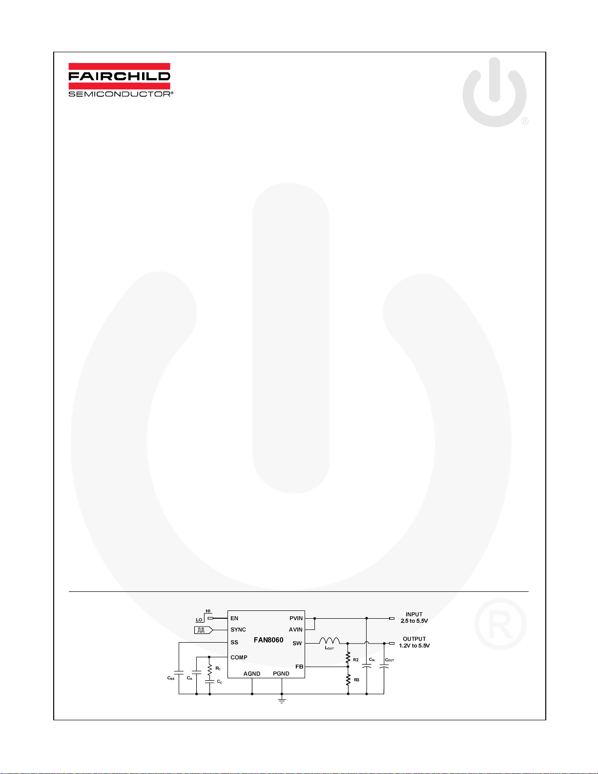
Application Diagram
Description
The FAN8060 is a highly efficient, monolithic, currentmode, step-down synchronous regulator. It can provide
1A continuous current from 2.5V to 5.5V input voltage.
The output voltage can be adjusted from 1.2V up to the
input voltage with an external voltage divider.
External compensation and soft-start allow for design
optimization and flexibility. High-frequency operation
allows for all-ceramic solutions and small footprints. In
addition, a user-selectable current limit provides
protection against output overload and short circuit.
FAN8060 features pulse skipping to achieve higher
efficiency during light load operation. 100% duty cycle
capability enables power solutions to extend the drop
out voltage.
Provision for external synchronization allows users to
minimize input capacitors and manage EMI in solutions.
FAN8060 is available in a green, low profile, 10-Lead
3x3mm MLP package.
Figure 1. Typical Application Circuit
© 2008 Fairchild Semiconductor Corporation www.fairchildsemi.com
FAN8060 • Rev. 1.0.0
Page 2
Ordering Information
FAN8060 — 1.2MHz, 1A Synchronous Step-Down DC/DC Regulator
Part Number
FAN8060EMPX -40 to +85°C Green
For Fairchild’s definition of “green” Eco Status, please vis i t : http://www.fairchildsemi.com/company/green/rohs_green.html.
Operating
Temperature Range
Eco Status
10-Pin, 3x3mm Molded
Leadless Package (MLP)
Package Packing Method
Tape & Reel
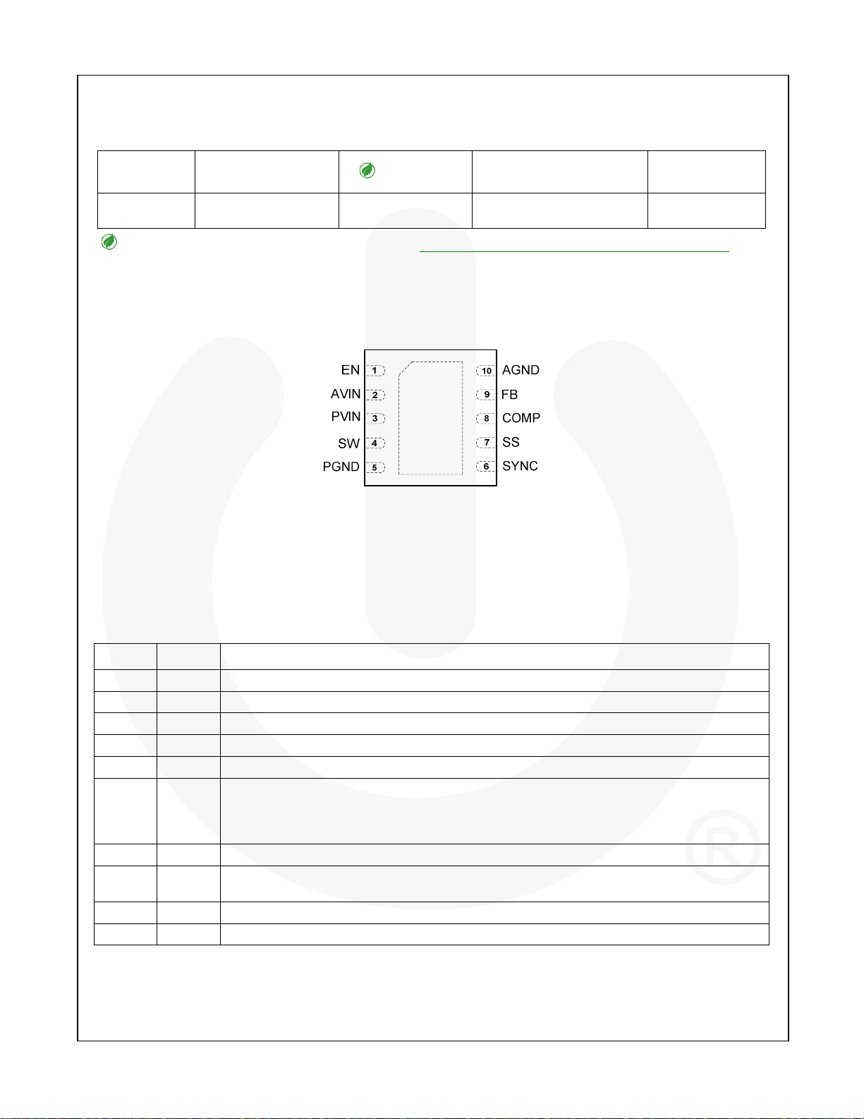
Pin Configuration
Figure 2. Pin Configuration (Top View)
Note:
1. Connect exposed PAD to AGND
Pin Definitions
Pin Name Function
1 EN
2 AVIN
3 PVIN
4 SW
5 PGND
6 SYNC
7 SS
8 COMP
9 FB
10 AGND
Enable. Enables operation when pulled to logic HIGH.
Analog Input Voltage. All internal control circuits are connected to this supply.
Power Input Voltage. Power stage supply voltage.
Switching Node. The drains of both PMOS and NMOS.
Power Ground. Power return and source of the power NMOS
Synchronization. Use this pin to synchronize the part to an external clock. This pin also
controls current limit threshold. Tie to ground for 1.0A or tie to V
current. When an external clock is applied, the default current setting is 1A. This pin has a
pull-down resistor of 450KΩ.
Soft-Start. A capacitor connected between this pin and AGND can set soft-start time.
Compensation. Error amplifier output. Connect the external compensation network between
this pin and AGND.
Output Voltage Feedback. Connect through a resistor divider to set the output voltage.
Analog Ground. Ground return for all internal control circuits.
for 0.5A continuous load
IN
© 2008 Fairchild Semiconductor Corporation www.fairchildsemi.com
FAN8060 • Rev. 1.0.0 2
Page 3
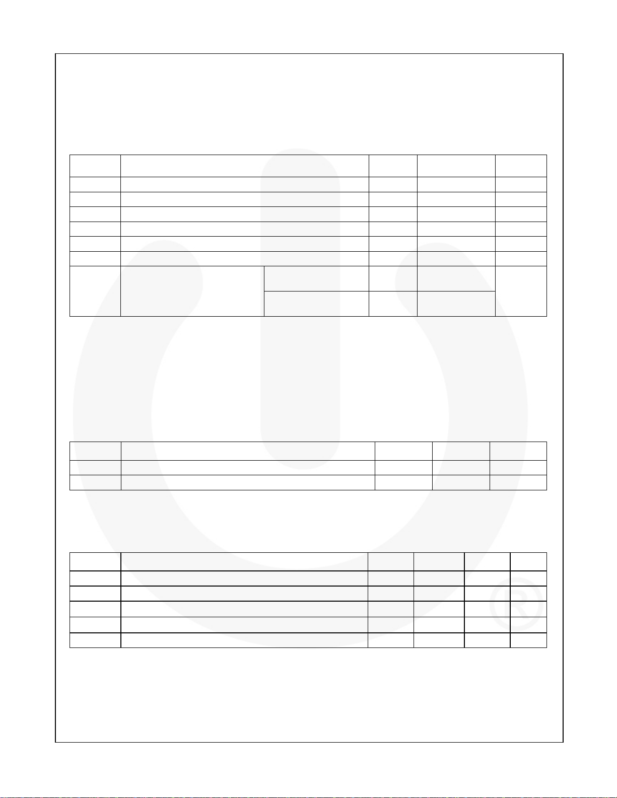
Absolute Maximum Ratings
Stresses exceeding the absolute maximum ratings may damage the device. The device may not function or be
operable above the recommended operating conditions and stressing the parts to these levels is not recommended.
In addition, extended exposure to stresses above the recommended operating conditions may affect device
reliability. The absolute maximum ratings are stress ratings only. All voltage values, except differential voltages, are
given with respect to the network ground terminal. Stress beyond those listed under Absolute Maximum Ratings may
cause permanent damage to the device.
Symbols Parameter Min. Max. Unit
V
PVIN (AGND=PGND) -0.3 6.0 V
PVIN
V
AVIN (AGND=PGND) -0.3 6.0 V
AVIN
VSW Switch Voltage, SW to GND -0.3 VIN + 0.3 or 6.0 V
All other pins except COMP -0.3 6.0 V
T
Storage Temperature -65 +150 °C
STG
TJ Junction Temperature -40 +125 °C
ESD Electrostatic Discharge Protection
Note:
2. COMP pin has an internal clamp to 1.5V.
Human Body Model,
JESD22-A114
Charged Device Model,
JESD22-C101
2.0
kV
2.5
FAN8060 — 1.2MHz, 1A Synchronous Step-Down DC/DC Regulator
Recommended Operating Conditions
The Recommended Operating Conditions table defines the conditions for actual device operation. Recommended
operating conditions are specified to ensure optimal performance to the datasheet specifications. Fairchild does not
recommend exceeding them or designing to Absolute Maximum Ratings.
Symbol Parameter Min. Max. Unit
VIN Supply Voltage 2.5 5.5 V
TA Ambient Operating Temperature -40 +85 °C
Thermal Information
Symbol Parameter Min. Typ. Max. Units
T
Storage Temperature -65 +150 °C
STG
TL Lead Soldering Temperature, 30 Seconds +300 °C
θJA
θJc
PD Total Power Dissipation in the package, TA=25°C
Note:
3. Typical thermal resistance when mounted on a four-layer PCB. Actual results are dependent upon mounting
method and surface related to the design.
Thermal Resistance: Junction-to-Ambient 49 °C/W
Thermal Resistance: Junction-to-Case
(3)
8 °C/W
(3)
1.3 W
© 2008 Fairchild Semiconductor Corporation www.fairchildsemi.com
FAN8060 • Rev. 1.0.0 3
Page 4
FAN8060 — 1.2MHz, 1A Synchronous Step-Down DC/DC Regulator
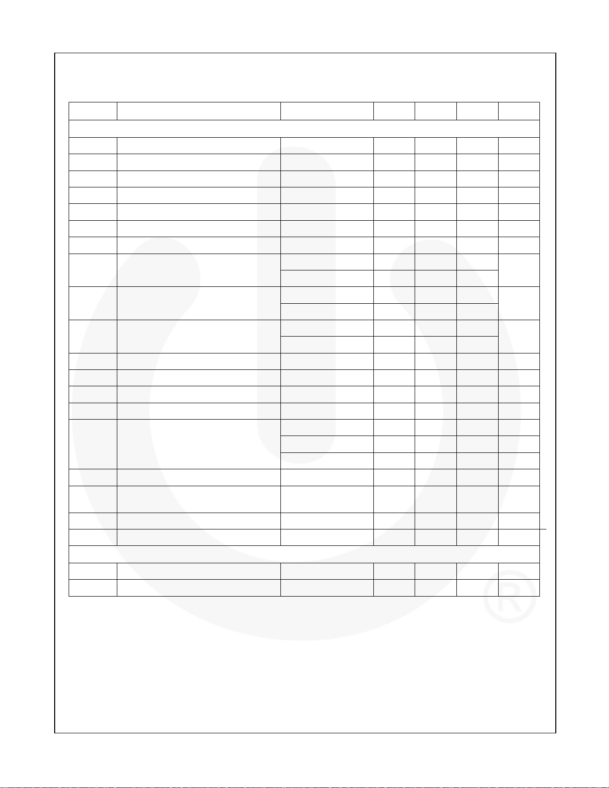
Electrical Characteristics
VIN=5.0V, V
Symbol Parameter Conditions Min. Typ. Max. Units
Basic Operation
VIN VIN Operating Voltage AVIN=PVIN 2.5 5.5 V
IQ Quiescent Current VEN=5 V, VSS=0V 250 371 500 µA
ISD Shutdown Current VEN=0V 0.34 0.60 µA
V
UVLO
V
UVLOHYS
V
ENH
V
ENL
R
ONPMOS
R
ONNMOS
I
LIM
f
Oscillator Frequency TA=25°C 1.105 1.21 1.35 MHz
OSC
V
SYNC
f
SYNC
t
SYNC
I
Error Amplifier
AMP
GCS Current Sense Gain
V
REF
IFB FB Bias Current TA=25°C -0.10 -0.06 0 µA
ISS Soft-Start Current -4.8 -4.5 -4.3 µA
=2.5 V, C
OUT
=10µF, CIN=10µF, over operating range, unless otherwise noted.
OUT
VIN Under-Voltage Lockout Rising VIN 2.10 2.19 2.25 V
VIN Under-Voltage Lockout Hysteresis 70 mV
Enable High Input Voltage 1.70 2.00 V
Enable Low Input Voltage 0.80 1.22 V
PMOS On Resistance
NMOS On Resistance
(4)
(4)
VIN=5V 200
V
=3.3V 300
IN
VIN=5V 200
mΩ
mΩ
VIN=3.3V 300
V
=0V 1.2
P-Channel Current Limit
=0.7V, VIN=5V, 100% Duty Cycle
V
FB
SYNC
V
SYNC=VIN
0.6
A
SYNC Threshold Rising Edge VIN/2 V
Synchronization Frequency V
Minimum SYNC Pulse Width V
=Square Wave 500 2000 KHz
SYNC
On Time 100 ns
SYNC
Sink/Source Current 30 45 60 µA
(4)
G
700 1000 1400 µA/V
EA
(4)
A
550 V/V
VEA
(4)
3 A/V
Reference Voltage for Temperature
Co-efficient, see Figure 12
Measured at FB Pin
=25°C
T
A
1.181 1.205 1.229 V
Protections
T
Over-Temperature Threshold
OTP
T
Over-Temperature Hysteresis +20 °C
HYS
(4)
+165 °C
Note:
4. Guaranteed by design and characterization; not production tested.
© 2008 Fairchild Semiconductor Corporation www.fairchildsemi.com
FAN8060 • Rev. 1.0.0 4
Page 5

Functional Block Diagram
FAN8060 — 1.2MHz, 1A Synchronous Step-Down DC/DC Regulator
SYNC
EN
4uA
SS
FB
450k
AVIN
& Ref erence
Vref
Enable
+
+
+
+
-
-
To Interna lSupply
GM
+
+
Slope
Compensation
1.4V
OTP
PWM
+
-
Short
Circuit
Protection
Oscillator
Pulse
Skip
+
Current
Sense
-
Log ic
&
Driver
+
-
Low Current
Detect
PVIN
SW
PGND
COMP AGND
Figure 3. Functional Block Diagram
© 2008 Fairchild Semiconductor Corporation www.fairchildsemi.com
FAN8060 • Rev. 1.0.0 5
Page 6

Operation Description
The FAN8060 is a step-down converter operating in
current-mode PWM architecture with a typical switching
frequency of 1.2MHz. At the beginning of each clock
cycle, the P-channel transistor is turned on. The current
in the inductor ramps up and is sensed via an internal
circuit. The P-channel switch is turned off when the
sensed current causes the PWM comparator to trip,
which is when the output voltage is in regulation or
when the inductor current reaches the current limit (set
internally to 1.2A, typically). After a minimum dead time
to prevent shoot-through current, the N-channel
transistor is turned on and the current ramps down. As
the clock cycle is completed, the N-channel switch is
turned off and the next clock cycle starts.
Soft Start
When the input voltage on AVIN exceeds the UVLO
threshold and EN is high, the circuit releases SS and
enables the PWM regulator. A capacitor connected to
the SS pin and AGND is charged by a 4μA internal
current source, causing the voltage on the capacitor to
rise. When this voltage reaches 1.2V, the output is in
regulation. The SS voltage continues to rise to AVIN.
The time for the output to reach regulation is given by
the following equation:
nFC
)(
mst
SS
)(
=
()
μ
VA
2.1/4
(1)
FAN8060 — 1.2MHz, 1A Synchronous Step-Down DC/DC Regulator
Light Load Operation
As the output load reduces, the current in the inductor
during off time is sensed across the low side MOSFET.
When the current reverses direction, the low-side
MOSFET is turned off and the high-side MOSFET is not
turned on until the output is out of regulation.
100% Duty Cycle Operation
As the input voltage approaches the output voltage, the
controller starts to increase the duty cycle to maintain
output regulation until duty cycle reaches 85%. The
controller then transitions to a 100% duty cycle mode
over several cycles to support the load. When the
dropout condition is met, the converter turns the Pchannel high side continuously on. In this mode, the
output voltage is equal to the input voltage, minus the
voltage drop across the P-channel MOSFET.
Output overload and short-circuit protection is active
during soft-start. When the part is disabled, SS pin is
pulled low internally.
Overload & Short-Circuit Protection
FAN8060 employs cycle-by-cycle current limiting, which
limits current by reducing duty cycle during overload. As
the load increases beyond the limit, the output voltage
starts to reduce, thereby reducing the FB voltage. When
the FB node is half the reference voltage and the
COMP node has reached maximum value, short-circuit
protection is detected. At that time, both the SS pin and
the COMP pin are pulled to ground until the inductor
current crosses zero. At that point, both SS and COMP
are released for the current to ramp up again. This
continues until the short-circuit condition is released.
© 2008 Fairchild Semiconductor Corporation www.fairchildsemi.com
FAN8060 • Rev. 1.0.0 6
Page 7

(
(
(
(
(
Typical Performance Characteristics
VIN=5V, V
EN(2V/div.)
VSW(2V/div.)
V
I
L
=2.4V, L=3.3µH, CIN=10µF, C
OUT
=10µF, fS=1.2MHz, TA=25°C, unless otherwise noted.
OUT
EN(2V/div.)
VSW(2V/div.)
V
(2V/div.)
(2V/div.)
OUT
(1A/div.)
[1ms/div.]
OUT
I
(1A/div.)
L
[1ms/div.]
Figure 4. EN Startup with 1A Load Figure 5. EN Turn off with 1A Load
FAN8060 — 1.2MHz, 1A Synchronous Step-Down DC/DC Regulator
VSW(2V/div.)
V
(2V/div.)
OUT
I
(1A/div.)
L
[500ns/div.]
VSW(2V/div.)
V
(2V/div.)
OUT
I
(1A/div.)
L
[200ns/div.]
Figure 6. PWM Operation with 1A Load Figure 7. 2MHz Sync Operation with 1A Load
V
(10mV/div. AC coupled)
OUT
V
(50mV/div. AC coupled)
OUT
VSW(2V/div.)
I
(500mA/div.)
OUT
Slew rate : 2.5A/us
I
(1A/div.)
L
[200µs/div.]
[500ns/div.]
Figure 8. Load Transient Response(Step-up/down) Figure 9. Output Voltage Ripple with 1A Load
© 2008 Fairchild Semiconductor Corporation www.fairchildsemi.com
FAN8060 • Rev. 1.0.0 7
Page 8

Typical Performance Characteristics (Continued)
VIN=5V, V
=2.4V, L=3.3µH, CIN=10µF, C
OUT
=10µF, fS=1.2MHz, TA=25°C, unless otherwise noted.
OUT
FAN8060 — 1.2MHz, 1A Synchronous Step-Down DC/DC Regulator
0.10
0.05
0.00
-0.05
-0.10
[%]
-0.15
OUT
V
5VIN/2.4V
-0.20
-0.25
-0.30
0 0 .2 0.4 0.6 0.8 1
Load Current [A]
Figure 10. Normalized V
[%]
REF
V
98
95
3.3VIN/2.4V
O
92
89
O
86
Efficiency [%]
5VIN/2.4V
83
80
00.20.40.60.81
Load Current [A]
vs. Load Current Figure 11. Efficiency vs. Load Current
OUT
4.00
2.00
0.00
-2.00
Frequency [%]
3.3VIN/2.4V
O
O
Figure 12. Normalized V
Temperature [℃]
vs. Temperature Figure 13. Normalized Oscillation Frequency vs.
REF
-4.00
-50 -25 0 25 50 75 100
Temperature [℃]
Temperature
© 2008 Fairchild Semiconductor Corporation www.fairchildsemi.com
FAN8060 • Rev. 1.0.0 8
Page 9

Applications Information
FAN8060 — 1.2MHz, 1A Synchronous Step-Down DC/DC Regulator
Refer to Figure 1 for reference designators.
Output Voltage Setting
The output voltage of the FAN8060 can be set from
1.2V to V
by an external resistor divider, given by the
IN
following equation:
R
2
)1(2.1
V
OUT
where, V
+=
R
3
equals the output voltage.
OUT
(2)
Inductor Selection
Typically, the inductor value is chosen based on ripple
current (ΔI
), which is chosen between 10% and 35% of
L
the maximum DC load. Regulator designs that require
fast transient response use a higher ripple-current
setting, while regulator designs that require higher
efficiency keep ripple current on the low side and
operate at a lower switching frequency.
For a given output voltage ripple requirement, L can be
calculated by the following equation:
DV
−⋅
OUT
L
≥
)1(
fI
⋅Δ
SL
(3)
where;
D = Duty ratio (VO/VIN);
fS = Switching frequency; and
∆IL = Inductor ripple value, typically set to 10% -
35% of the maximum steady-state load current.
The inductor should have a low DCR to minimize the
conduction losses and maximize efficiency. Some
recommended inductors are suggested in Table 1:
Table 1. Recommended Inductors (3.3µH)
Size[mm2] DCR Part Number Vendor
7x7x3
5x5x2
4x4x2
2.6x2.8x1.2
23mΩ
60mΩ
78mΩ
130mΩ
SLF7032T-3R3 TDK
LTF5022T-3R3 TDK
VLCF4020T-3R3 TDK
VLF3012AT-3R3 TDK
Output Capacitor Selection
The output capacitor is selected based on the needs of
the final application and its output ripple requirements.
A larger output capacitor value reduces the output
ripple voltage. The formula of output ripple ΔV
where C
⎛
⎜
+Δ≅Δ
ESRIV
LOUT
⎜
8
⎝
is the output capacitor.
OUT
⎞
1
⎟
⎟
⋅⋅
fC
SOUT
⎠
ESR is the equivalent series resistance of the output
capacitor.
OUT is:
(4)
Input Capacitor Selection
The input capacitor reduces the RMS current drawn
from the input and switching noise from the device. The
combined RMS current rating for the input capacitor
should be greater than the value calculated by the
following equation:
2
)(
DDII
OUTMAXRMS
−⋅=
(5)
where:
I
I
= RMS current of the input capacitor; and
RMS
OUTMAX =
Maximum output current.
Small, high value, inexpensive, lower-ESR ceramic
capacitors are recommended; 10µF ceramic capacitors
with X7R or X5R should be adequate for 1A applications.
Loop Compensation
The loop is compensated using a feedback network
connected between COMP and AGND. Figure 14
shows a Type-2 compensation network used to
stabilize the FAN8060.
Vout
R2
VFB
-
R3
Gm
+
Vref
Figure 14. Compensation Network
The goal of the compensation design is to shape the
frequency response of the converter to achieve high
DC gain and fast transient, while maintaining loop
stability. FAN8060 employs peak-current-mode control
for easy use and fast transient response. Current mode
control helps simplify the loop to a one-pole and one
zero system.
The DC gain of the voltage feedback loop is given by:
V
FB
V
OUT
AGRA ⋅⋅⋅=
VEACSLVDC
where:
A
= DC gain of the feedback loop;
VDC
= Load resistor value (V
R
L
G
= Current sense gain (3A/V);
CS
= Error amplifier voltage gain (550V/V); and
A
VEA
V
= Feedback threshold voltage (1.2V).
FB
RC
CC
OUT/IOUT
Ve
CA
(6)
);
© 2008 Fairchild Semiconductor Corporation www.fairchildsemi.com
FAN8060 • Rev. 1.0.0 9
Page 10

The system pole is calculated by the equation:
1
=
P
1
π
2
RCf⋅⋅
LOUT
(7)
The system zero is due to the output capacitor and its
ESR. System zero is calculated by the equation:
f
=
z
1
1
π
2
OUT
ESRC
⋅⋅
(8)
The output characteristics of the error (Gm) amplifier
are controlled by a series capacitor and resistor
network connected at the COMP pin to GND.
The pole is calculated by the following equation:
G
EA
f⋅⋅=
p
2
π
2
AC
VEAC
(9)
where:
GEA = Error Amplifier Transconductance (1000µA/V);
and
C
= compensation capacitor.
C
Zero is due to the compensation capacitor (CC) and
resistor (R
2
z
) calculated by the following equation:
C
1
=
π
2
RCf⋅⋅
CC
(10)
where RC is compensation resistor.
The system crossover frequency (fC), where the control
loop has unity gain, is recommended to be set at 1/10
of switching frequency. Generally, higher f
C
th
means
faster response to load transients, but can result in
instability if not properly compensated.
The first step in compensation design is choosing the
compensation resistor (R
) to set the crossover
C
frequency by the following equation:
π
2
R
=
C
where V
is reference voltage.
FB
VfC
⋅⋅⋅
OUTCOUT
VGG
⋅⋅
FBEACS
(11)
The next step is choosing the compensation capacitor
(C
) to achieve the desired phase margin. For
C
applications with typical inductor values, setting the
compensation zero, f
, to below one fourth of the
Z2
crossover frequency provides sufficient phase margin.
Determine the (C
2
=
C
π
) value by the following equation:
C
fRC⋅⋅
CC
(12)
Then determine if the second compensation capacitor
(C
) is required. It is required if the ESR zero of the
A
output capacitor is located at less than half of the
switching frequency.
1
π
OUT
f
S
ESRC<⋅⋅
22
(13)
If required, add the second compensation capacitor
(C
) to set the pole f
A
Determine (C
ESRCC⋅
OUT
=
A
R
C
) value by the equation:
A
at the location of the ESR zero.
P3
Design Example
Table 2 provides component values for delivering
various output voltages with loads up to 1A with V
5V (+/-10% tolerance).
Table 2. Recommended Feedback and
Compensation Values (V
C4 L1 R2 R3 R1 C5 C2
V
O
1.2V Short Open
1.5V
1.8V
2.5V
3.3V
10µF 3.3µH
2.55kΩ 10.2kΩ
5.9kΩ 11.8kΩ
16.2kΩ 15kΩ
18.7kΩ 10.7kΩ
Figure 15. Recommended Schematic (5VIN to 2.5VO)
=5V)
IN
4.7kΩ
1.5nF 150pF
(14)
at
IN
FAN8060 — 1.2MHz, 1A Synchronous Step-Down DC/DC Regulator
© 2008 Fairchild Semiconductor Corporation www.fairchildsemi.com
FAN8060 • Rev. 1.0.0 10
Page 11

PCB Layout Recommendations
The switching power supply PCB layout needs careful
attention and is critical to achieving low losses and
clean and stable operation. Although each design is
different, below are some general recommendations for
a good PCB layout.
Keep the high-current traces and load connectors
as short and wide as possible. These traces
consist of VIN, GND, VOUT, and SW.
Place the input capacitor, the inductor, and the
output capacitor as close as possible to the IC
terminals.
Keep the loop area between SW node, inductor,
and output capacitors as small as possible;
minimizing ground loops to reduce EMI issues.
Route high-dV/dt signals, such as SW node, away
from the error amplifier input/output pins.
Keep components connected to the FB and COMP
pins close to the pins.
Figure 16. Recommended PCB Layout
FAN8060 — 1.2MHz, 1A Synchronous Step-Down DC/DC Regulator
© 2008 Fairchild Semiconductor Corporation www.fairchildsemi.com
FAN8060 • Rev. 1.0.0 11
Page 12

Physical Dimensions
FAN8060 — 1.2MHz, 1A Synchronous Step-Down DC/DC Regulator
2X
0.8 MAX
0.10
C
0.08 C
SEATING
PLANE
PIN #1 IDENT
0.15 C
0.05
0.00
3.0
TOP VIEW
SIDE VIEW
(3.00±0.10)
2.25±0.05
(0.38)
1
0.50
6
3.10
1.55
2.00
0.25
5
3.0
A
B
2X
0.15 C
D
0.23
10
2.25
2.20
2.00
0.55
0.78
2.33
0.02
1
RECOMMENDED LAND PATTERN
(0.20)
C
5
6
(3.00±0.10)
0.10 CAB
0.05
C
1.55±0.05
0.40±0.05
0.5
10
2.0
0.30
0.20
BOTTOM VIEW
A. CONFORMS TO JEDEC REGISTRATION MO-229,
VARIATION WEED-5
B. DIMENSIONS ARE IN MILLIMETERS.
C. DIMENSIONS AND TOLERANCES PER
ASME Y14.5M, 1994
D. LAND PATTERN DIMENSIONS ARE NOMINAL
REFERENCE VALUES ONLY
MLP10BrevA
Figure 17. 10-Pin, 3x3mm Molded Leadless Package (MLP)
Package drawings are provided as a service to customers considering Fairchild components. Drawings may change in any manner
without notice. Pl ease note the revision and/or date on t he drawing and contact a Fairchild S emiconductor representative to v er ify
or obtain the most recent revision. Package specifications do not expand the terms of Fairchild’s worldwide terms and conditions, specifically
the warranty therein, which covers Fairchild products.
Always visit Fairchild Semiconductor’s online packaging area for the most recent package drawings:
http://www.fairchildsem i.com/p ackagi ng/
.
© 2008 Fairchild Semiconductor Corporation www.fairchildsemi.com
FAN8060 • Rev. 1.0.0 12
Page 13

FAN8060 — 1.2MHz, 1A Synchronous Step-Down DC/DC Regulator
© 2008 Fairchild Semiconductor Corporation www.fairchildsemi.com
FAN8060 • Rev. 1.0.0 13
 Loading...