

Page 1
EM MICROELECTRONIC - MARIN SA
EM4450
EM4550
1 KBit Read/Write Contactless Identification Device
Description
The EM4450/4550 is a CMOS integrated circuit intended
for use in electronic Read/Write RF Transponders. The
difference between EM4450 and EM4550 is that EM4550
are bumped and has megapads for the two coils. The chip
contains 1 KBit of EEPROM which can be configured by
the user, allowing a write inhibited area, a read protected
area, and a read area output continuously at power on.
The memory can be secured by using the 32 bit password
for all write and read protected operations. The password
can be updated, but never read. The fixed code serial
number and device identification are laser programmed
making every chip unique.
The EM4450/4550 will transmit data to the transceiver by
modulating the amplitude of the electromagnetic field, and
receive data and commands in a similar way. Simple
commands will enable to write EEPROM, to update the
password, to read a specific memory area, and to reset
the logic.
The coil of the tuned circuit is the only external component
required, all remaining functions are integrated in the chip.
Features
1 KBit of EEPROM organized in 32 words of 32 bits
32 bit Device Serial Number (Read Only Laser ROM)
32 bit Device Identification (Read Only Laser ROM)
Power-On-Reset sequence
Power Check for EEPROM write operation
User defined Read Memory Area at Power On
User defined Write Inhibited Memory Area
User defined Read Protected Memory Area
Data Transmission performed by Amplitude Modulation
Two Data Rate Options 2 KBd (Opt64) or 4 KBd (Opt32)
Bit Period = 64 or 32 periods of field frequency
170 pF ± 2% on chip Resonant Capacitor
-40 to +85°C Temperature range
100 to 150 kHz Field Frequency range
On chip Rectifier and Voltage Limiter
No external supply buffer capacitance needed due to
low power consumption
Available in chip form for mass production and PCB and
CID package for samples.
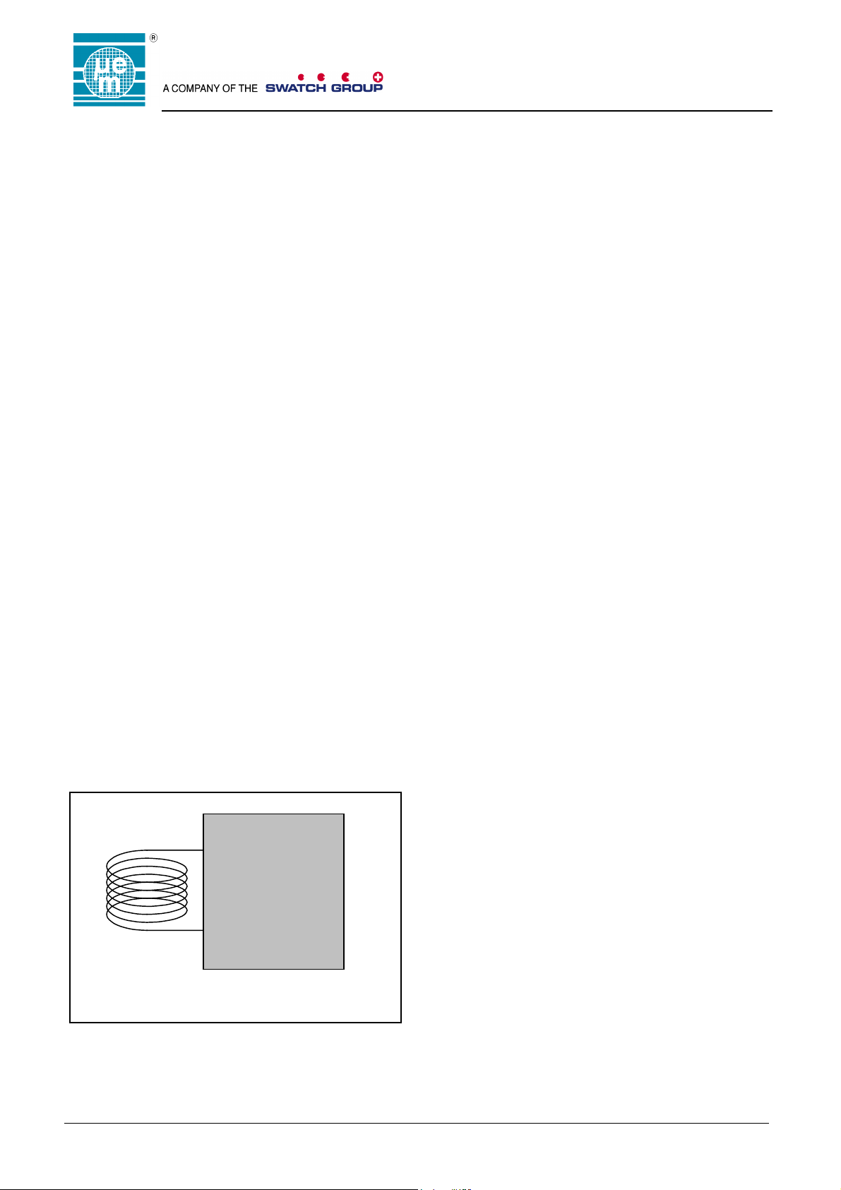
Typical Operating Configuration
Coil2
L
EM4450
Coil1
Typical value of inductance at 125 kHz is 9.6 mH
Applications
Ticketing
Automotive Immobilizer with rolling code
High Security Hands Free Access Control
Industrial automation with portable database
Manufacturing automation
Prepayment Devices
Copyright 2003, EM Microelectronic-Marin SA
Fig.1
1 www.emmicroelectronic.com
Page 2
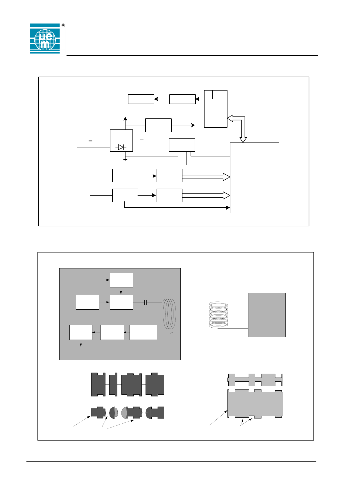
Block Diagram
EM4450
EM4550
coil2
coil1
System Principle
Modulator Encoder
+V
AC/DC
C
r
converter
Clo ck
Ex t r ac t o r
Data
Ex t r ac t o r
Voltage
Regu lato r
C
s
Sequencer
Command
Po w e r
Control
Dec oder
ROM
EEPROM
Res et
Write Enable
Control
Logic
Fig. 2
Data to be sent
to transponder
Osc illator
Dat a
Dec od er
Data rece ive d
from
transponder
Sig nal on
Tr ansceiver coi l
Sig nal on
Tr ansponder coil
RF Carrier
Transceiver
Mo du la to r
Antenna
Filte r &
Gain
Driv er
RECEIVE M ODE
Data
Demodulator
Transponder
Coil 1
EM4450
Sig nal on
Tr ansponder coi l
Sig nal on
Transceiver coil
RF Carrier
Coil 2
READ M ODE
Data
Copyright 2003, EM Microelectronic-Marin SA
Fig. 3
2 www.emmicroelectronic.com
Page 3
EM4450
pp
EM4550
Absolute Maximum Ratings
Parameter Symbol Conditions
Maximum AC peak Current
induced on COIL1 and COIL2
Power Supply
Maximum Voltage other pads
Minimum Voltage other pads
Storage temperature T
Electrostatic discharge
maximum
to MIL-STD-883C method
3015
Stresses above these listed maximum ratings may cause permanent damages to the device. Exposure beyond specified
operating conditions may affect device reliability or cause malfunction.
Handling Procedures
This device has built-in protection against high static voltages or electric fields; however, anti-static precautions must be
taken as for any other CMOS component. Unless otherwise specified, proper operation can only occur when all terminal
voltages are kept within the voltage range. Unused inputs must always be tied to a defined logic voltage level.
I
V
V
V
V
COIL
DD
max
min
store
ESD
± 30 mA
-0.3 to 3.5 V
+0.3V
V
DD
VSS-0.3V
-55 to +125°C
2000V
Operating Conditions
Parameter Symbol Min Max Unit
Operating Temperature T
Maximum coil current I
AC Voltage on Coil V
Supply Frequency f
COIL
-40 +85 °C
op
coil
100 150 kHz
coil
10 mA
note 1
V
note 1: Maximum voltage is defined by forcing 10mA on Coil1 - Coil2.
Electrical Characteristics
VDD =2.5V, VSS =0V , f
Parameter Symbol Conditions Min Typ Max Unit
Supply Voltage V
Minimum EEPROM write
voltage
Power Check EEPROM write I
Supply current / read I
Suppy current / write I
Modulator ON voltage drop V
Monoflop T
Resonance Capacitor C
Powercheck level V
Power On Reset level high V
Clock extractor input min.
Clock extractor input max.
EEPROM data endurance N
EEPROM retention T
= 125 kHz Sine wave , V
coil
DD
V
DDee
PWcheck
rd
wr
ON
mono
PWcheck
prh
V
clkmin
V
clkmax
cy
ret
r
V
Max. Voltage to detect modulation stop
Top = 55°C after 100'000 cycles (note 2) 10 years
= 1Vpp , Top = 25°C , unless otherwise specified
coil
2.3 3.2 V
2V
VDD = 2.8V 32
Read Mode 3
Write mode (VDD = 2.8V) 22
(COIL1 - VSS)
V
(COIL1 - VSS)
& V
(COIL2 - VSS) Icoil
& V
(COIL2 - VSS) Icoil
= 100µA
= 5 mA
0.50
2.50
35 85
166.6 170 173.4 pF
22.7V
Rising Supply 1 1.5 V
Minimum Voltage for Clock Extraction
0.25
25
Erase all / Write all at VDD = 3.5 V 100'000 cycles
V
mV
µA
µA
µA
V
V
µs
pp
pp
note 2: Based on 1000 hours at 150°C
Copyright 2003, EM Microelectronic-Marin SA
3 www.emmicroelectronic.com
Page 4
EM4450
EM4550
Timing Characteristics
VDD =2.5V, VSS=0V , f
All timings are derived from the field frequency and are specified as a number of RF periods..
Parameter Symbol Conditions Value Unit
Option : 64 clocks per bit
Read Bit Period t
LIW/ACK/NACK pattern duration t
Read 1 Word Duration t
Processing Pause Time t
Write Access Time t
Initialization Time t
EEPROM write time t
Option : 32 clocks per bit
Read Bit Period t
LIW/ACK/NACK pattern duration t
Read 1 Word Duration t
Processing Pause Time t
Write Access Time t
Initialization Time t
EEPROM write time t
RF periods represent periods of the carrier frequency emitted by the transceiver unit. For example, if 125 kHz is used :
The Read bit period (Opt64) would be : 1/125'000*64 = 512 µs, and the time to read 1 word : 1/125'000*3200 = 25.6 ms.
The Read bit period (Opt32) would be : 1/125'000*32 = 256 µs, and the time to read 1 word : 1/125'000*1600 = 12.8 ms.
= 125 kHz Sine wave, V
coil
Opt64
rdb
patt
rdw
pp
wa
init
wee
Opt32
rdb
patt
rdw
pp
wa
init
wee
= 1Vpp , Top = 25°C unless otherwise specified
coil
64 RF periods
320 RF periods
including LIW 3200 RF periods
64 RF periods
64 RF periods
2112 RF periods
VDD = 3V 3200 RF periods
32 RF periods
160 RF periods
including LIW 1600 RF periods
32 RF periods
32 RF periods
1056 RF periods
VDD = 3V 2624 RF periods
ATTENTION
Due to amplitude modulation of the coil-signal, the clock-extractor may miss clocks or add spurious clocks close
to the edges of the RF-envelope. This desynchronisation will not be larger than ±3 clocks per bit and must be
taken into account when developing reader software.
Functional Description
General
The EM4450/4550 is supplied by means of an electromagnetic field induced on the attached coil. The AC voltage is rectified
in order to provide a DC internal supply voltage. When the DC voltage crosses the Power-On level, the chip enters the
Standard Read Mode and sends data continuously. The data to be sent in this mode is user defined by storing the first and
last addresses to be output. When the last address is sent, the chip will continue with the first address until the transceiver
sends a request. In the read mode, a Listen Window (LIW) is generated before each word. During this time, the
EM4450/4550 will turn to the Receive Mode (RM) if it receives a valid RM pattern. The chip then expects a valid command.
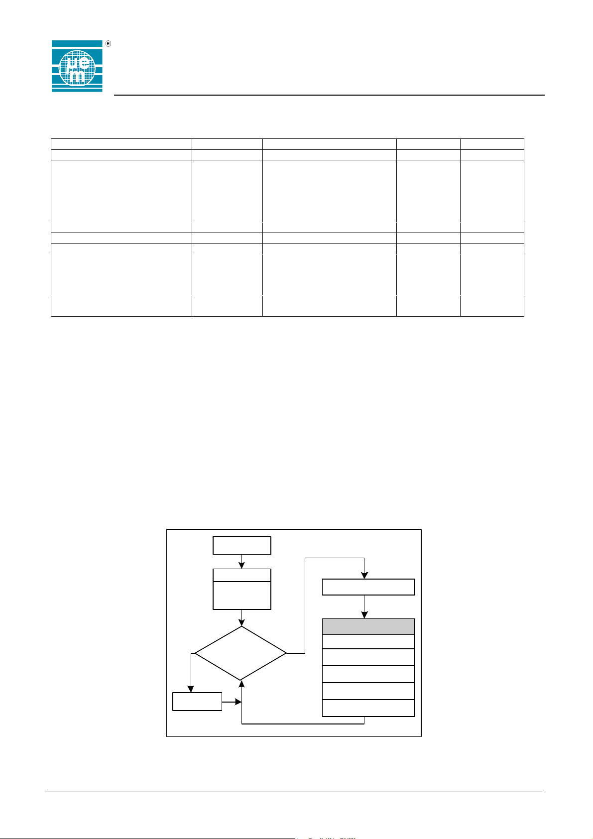
Mode of Operation
Po w e r - On
Ini t
Standard
Ge t Comma n d
Read Mode
Execute Command
Rec eiv e
Mode
request ?
YESNO
Login
Write Word
Write Password
Selective Read
Send w ord
Reset
Copyright 2003, EM Microelectronic-Marin SA
Fig. 4
4 www.emmicroelectronic.com
Page 5
EM4450
EM4550
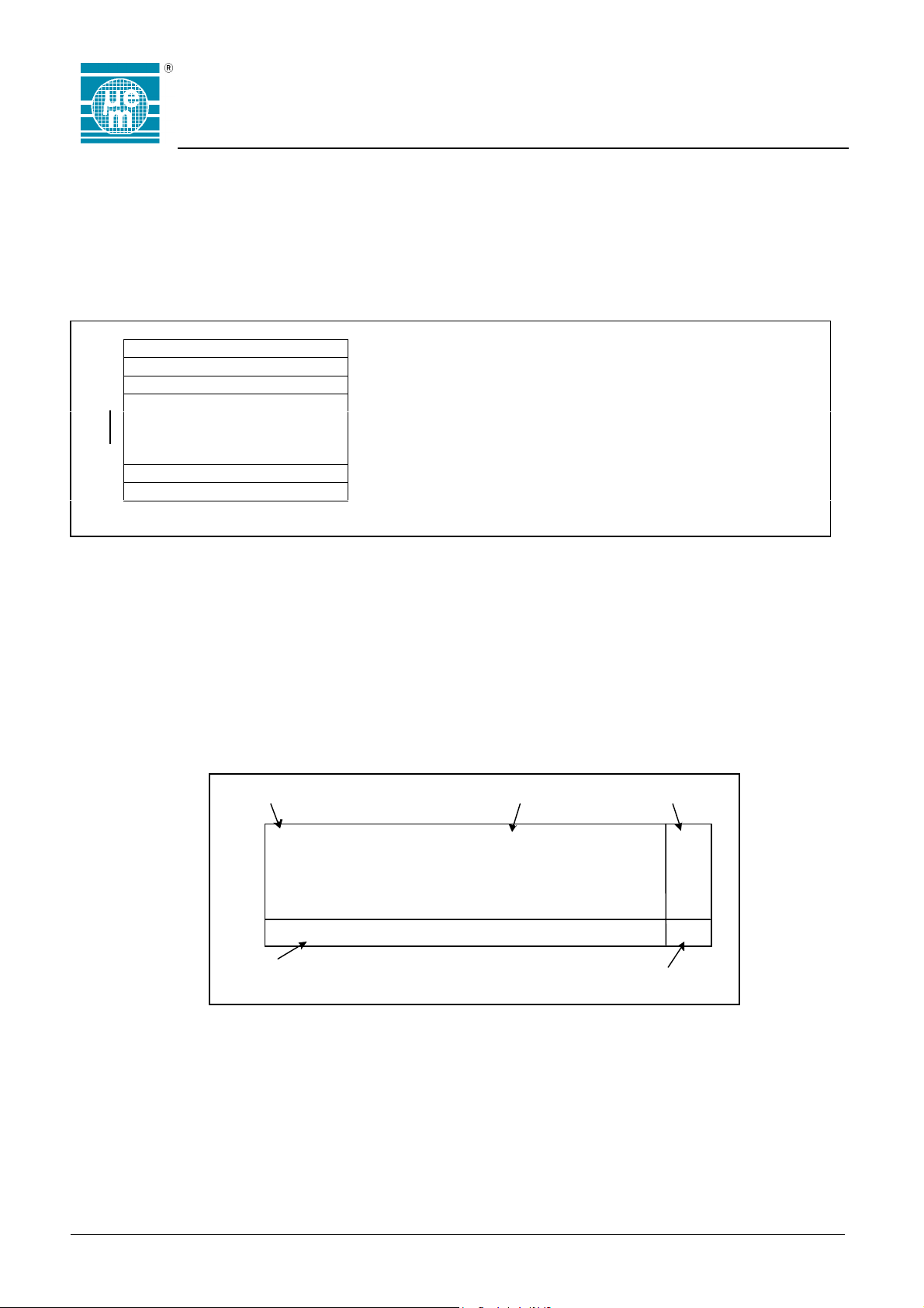
Memory Organisation
The 1024 bit EEPROM is organised in 32 words of 32 bits. The first three words are assigned to the Password, the
Protection word, and the Control word. In order to write one of these three words, it is necessary to send the valid
password. At fabrication, the EM4450/4550 comes with all bits of the password programmed to a logic "0". The Password
cannot be read out. The memory contains two extra words of Laser ROM. These words are laser programmed during
fabrication for every chip, are unique and cannot be altered.
Memory Map
Bit 0 ------------------------------ Bit 31
Word 0 PASSWORD EE
1
PROTECTION WORD EE 0 – 7 First Word Read 0 – 7 First Word Read Protected
CONTROL WORD EE 8 – 15 Last Word Read 8 – 15 Last Word Read Protected
3
928 Bits of USER 17 Read After Write On/Off 24 – 31 Last Word Write Inhibited
EEPROM 18 – 31 User available
31
32 DEVICE SERIAL NUMBER Laser Write Only – No Read Access
33 DEVICE IDENTIFICATION Laser On means bit set to logic '1'
EE 16 Password Check On/Off 16 – 23 First Word Write Inhibited
Control Word Protection Word
Password
Device Identification Word &
Off means bit set to logic '0'
Serial Number Word
Laser Programmed – Read only
Fig.5
Standard Read Mode
After a Power-On-Reset and upon completion of a command, the chip will execute the Standard Read Mode, in which it will
send data continuously, word by word from the memory section defined between the First Word Read (FWR) and Last
Word Read (LWR). When the last word is output, the chip will continue with the first word until the transceiver sends a
request. If FWR and LWR are the same, the same word will be sent repetitively. The Listen Window (LIW) is generated
before each word to check if the transceiver is sending data. The LIW has a duration of 320 (160 opt 32) periods of the RF
field. FWR and LWR have to be programmed as valid addresses (FWR ≤ LWR and ≤ 33).
The words sent by the EM4450/4550 comprise 32 data bits and parity bits. The parity bits are not stored in the EEPROM,
but generated while the message is sent as described below. The parity is even for rows and columns, meaning that the
total number of "1's" is even (including the parity bit).
Word organisation (Words 0 to 33)
First bit output
D0 D1 D2 D3 D4 D5 D6 D7 P0
D8 D9 D10 D11 D12 D13 D14 D15 P1
D16 D17 D18 D19 D20 D21 D22 D23 P2
D24 D25 D26 D27 D28 D29 D30 D31 P3
PC0 PC1 PC2 PC3 PC4 PC5 PC6 PC7 0
Column Even Partiy
Data Row Even Parity
Last bit output
logic '0'
Fig. 6
When a word is read protected, the output will consist of 45 bits set to logic "0". The password has to be used to output
correctly a read protected memory area.
Copyright 2003, EM Microelectronic-Marin SA
5 www.emmicroelectronic.com
Page 6

Read Sequence
EM4450
EM4550
POR
INIT
OUTPUT
T0 periods :
32 32 128 64 64 (Opt64)
16 16 64 32 32 (Opt32)
LIW FWR LIW FWR+1 LWR LIW FWR LIWLIWLIW
LIW D0-D7 P0 D8-D15 P1 D16-D23 P2 D24-D31 P3 PC0-PC7 "0"
1 bit = 64 T0 periods (Opt64)
32 T0 periods (Opt32)
Data
Coded Data
T0 = Period of RF carrier
frequency
1 bit
1 bit
1 bit 1 bit
Fig. 7
Receive Mode
To activate the Receive Mode, the Transceiver sends to the chip the RM pattern (while in the modulated phase of a Listen
Window LIW). The EM4450/4550 will stop sending data upon reception of a valid RM. The chip then expects a command.
The RM pattern consists of 2 bits "0" sent by the transceiver. The first bit "0" transmitted is to be detected during the 64 (32
opt 32) periods where the modulation is "ON" in LIW.
output
WORD n LIW
input
RM COMMAND
Fig. 8
Commands
The commands are composed of nine bits : eight data bits and one even parity bit (total amount of "ones" is even including
the parity bit).
COM M AND BITS FUNCTION
0 0 0 0 0 0 0 1 1 LOGIN
0 0 0 1 0 0 0 1 0 WRITE PASSWORD
0 0 0 1 0 0 1 0 0 WRITE WORD
0 0 0 0 1 0 1 0 0 SELECTIVE READ MODE
1 0 0 0 0 0 0 0 1 RESET
First bit Received Parity bit
Fig. 9
Copyright 2003, EM Microelectronic-Marin SA
6 www.emmicroelectronic.com
Page 7

EM4450
A
A
A
EM4550
Selective Read Mode
The Selective Read Mode is used to read other data than that defined between FWR and LWR. To enter Selective Read
Mode, the Transceiver has to send during LIW a Receive mode pattern (RM) to turn the EM4450/4550 in Receive Mode.
Then the Selective Read Mode Command is sent by the transceiver followed by the First and Last addresses to be read.
The FWR and LWR are then replaced by the new addresses and the chip is operating in the same way as the Standard
Read Mode. The control word is not modified by this command, and the next standard read mode operation will work with
original FWR and LWR (Selected area is read once and then the chip returns to Standard Read Mode).
To read words which are Read Protected, a Login command has to be sent by the transceiver prior to the Selective Read
command. The Login command is to be used only once for all subsequent commands requiring a password.
The Selective Read mode command is followed by a single 32-bit word containing the new first and last addresses. Bits 0
to 7 correspond to the First Word Read and bits 8 to 15 correspond to the Last Word Read. Bits 16 to 31 have to be sent
but are not used in the chip. The parities must be sent according to the word organisation as described in fig.7. Note that
bit 31 is transmitted first.
To read the device Identification or the Serial Number, the Selective Read Command allows direct access to the Laser
programmed words. These words can also be addressed in the standard read mode by selecting the addresses
accordingly.
output
input
WORD n LIW
RM Selective RD ADDRESSES
First bit receiv ed
XX XX XX XX XX XX XX XX P3 XX XX XX XX XX XX XX XX P2
LW7 LW 6 LW5 LW4 LW3 LW2 LW1 LW0 P1 FW 7 FW6 FW 5 FW 4 FW3 FW 2 FW 1 FW0 P0 PC7 PC6 PC5 PC4 PC3 PC2 PC1 PC0 "0"
Addresses Bit Stream Fo rmat
CK/NAK LIW LIW FWR LIW
t
pp
Fig. 10
Fig. 11
Reset Command
The Reset Command will return from any mode to the Standard Read Mode. The next word out is the FWR.
output
input
WORD n LIW
RM RESET
t
CK/NAK
pp
LIW LIW FWR LIW
t
init
Fig. 12
Login
The Login command is used to access protected memory areas. This command has to be used only once to perform
several password protected commands. The Power-On-Reset sequence and the Reset command will reset the password
entry, and a new Login command has to be received to perform further password protected operations.
Upon reception of a correct password, the EM4450/4550 will respond with an acknowledge pattern (ACK) and then
continue in Standard Read Mode. If the Login is correct then password protected operations are allowed. If the password is
incorrect, a NAK pattern is issued and password protected operations will not be possible (refer to Write Word for password
data structure).
output
input
Copyright 2003, EM Microelectronic-Marin SA
WORD n LIW
RM LOGIN PASSWORD
CK/NAK LIW LIW FWR LIW
t
pp
Fig. 13
7 www.emmicroelectronic.com
Page 8
EM4450
A
A
A
EM4550
If bit 16 of the control word is disabled (Password Check ON/OFF), the Login is still mandatory to modify the Protection
Word, the Control Word, and the Password, but not to write in the EEPROM which is not write inhibited. In order to modify a
write inhibited word, the Protection word has to be modified first. The Read protected area always requires the Login to be
read. If the Write Protection Word is write protected, the write protection configuration is locked.
Write Password
When a Write Password command is received, the chip next expects information on the actual valid password. The chip
sends back an ACK pattern if the password is correct. Then the chip expects the new password consisting of 32 bits +
parity bit to be stored in the EEPROM. The chip will respond with an ACK pattern for a correct reception of data upon
reception of the new password, and then will send another acknowledge pattern (ACK) to announce that the data is stored
in the EEPROM. The Read after Write function has no effect on this command. If the password is wrong or the transmission
is faulty, the chip will : send a NAK pattern; return to the Standard Read Mode; and, the password will remain the same.
(Refer to Write Word for password data structure).
output
input
WORD n LIW
RM WRITE PW ACTUAL PW
t
pp
CK LIW
RM NEW PW
t
wa
TRANSCEIVER RF FIELD "ON"
CK
t
wee
CK LIW LIW FWR
Fig. 14
Write Word
The Write mode allows modification of the EEPROM contents word by word. To modify address 1 (Protection word) and
address 2 (Control word), it is mandatory to first send a Login command in order to Log in (like in a computer). The new
written values will take effect only after performing a Reset command. It is strongly recommended to check the result of
modifying the contents of these addresses effecting the function of the chip. Address 0 (Password) cannot be modified with
this command but can be changed with the Write Password command.
Addresses 3 to 31 are programmable according to the defined protections. If the Password Check bit is off (bit 16 of control
word) and the word is not write inhibited, the selected word can be freely modified without password. If the Password Check
bit is on and the word is not write inhibited, the selected word can be modified with a previous Login. In any case, if the
word is write inhibited, the protection word has to be changed before programming can occur.
Write to Address Check Password bit
(bit 16 / Control word)
Write Inhibit
(Protection word)
Write Operation
0 X X Only with Write Password
command
1 – 2 X OFF Login always required
1 – 2 X ON Write configuration LOCKED
3 – 31 OFF OFF Freely programmable
3 – 31 ON OFF Login required
3 – 31 X ON Change protection word first
The Write Word command is followed by the address and data. The address consists of a 9 bit block containing 8 data bits
and 1 even parity bit. Only 6 bits from the data section are used for the word addressing, and the first three bits sent must
be "0". The data consists of 4 times 9 bit blocks, each block consisting of 8 data bits and 1 associated even parity bit and
one additional block consisting of 8 column parity bits and "0" as stop bit (Refer to fig. 7)
Address
0 0 A5 A4 A3 A2 A1 A0
Padd
First bit received
Data
D31 D30 D29 D28 D27 D26 D25 D24 P3 D23 D22 D21 D20 D19 D18 D17 D16 P2 D15 D14
D13 D12 .......................... D02 D01 D00 P0 PC7 PC6 PC5 PC4 PC3 PC2 PC1 PC0 "0"
Copyright 2003, EM Microelectronic-Marin SA
8 www.emmicroelectronic.com
Note :
A5 in write mode always "0"
(addresses Laser ROM)
Fig. 15
Page 9

EM4450
A
EM4550
After reception of the command, the address, and the data, the EM4450/4550 will check the parity, the write protection
status, the Login status, and also if the available power from the RF field is sufficient. If all the conditions are satisfied, an
acknowledge pattern (ACK) will be issued afterward and the EEPROM writing process will start. At the end of programming,
the chip will send an Acknowledge pattern (ACK). If at least one of the checks fails, the chip will issue a no acknowledge
pattern (NAK) instead of ACK and return to the Standard Read Mode. The Transceiver will keep the RF field permanently
"ON" during the whole writing process time.
The Read After Write function (bit 17 of Control word) controls the mode of operation following a write operation. When
"ON" the latest written word will be read out and output next to the ACK pattern and two Listen Windows (LIW-LIW) even if
the word is read protected. When "OFF", the ACK is followed immediately by a LIW-LIW and FWR. The last written word is
not output.
If a request from the transceiver to return in receive mode (RM) is generated during the LIW, another word can be written in.
Otherwise, the EM4450/4550 will return in the Standard Read Mode.
Write 1 word
WORD n LIW ACK LIW LIW FWRoutput
input
Write severalwords
WORD n LIWoutput
input
Read After Write function
WORD n LIW
input
RM WRITE WORD ADDRESS DATA
RM WRITE WORD ADDRESS DATA
RM WRITE WORD ADDRESS DATA
t
wa
TRANSCEIVER RF FIELD "ON"
t
wa
TRANSCEIVER RF FIELD "ON"
t
wa
TRANSCEIVER RF FIELD "ON"
ACK
ACK
t
wee
t
wee
ACK LIW ACK
RM WRITE WORD ADDRESS DATA
t
wee
CK LIW LIW Last Written LIW LIW FWRoutput
Write not allowed or wrong transmission
WORD n LIW NACK LIW LIW FWRoutput
input
Copyright 2003, EM Microelectronic-Marin SA
RM WRITE WORD ADDRESS DATA
t
wa
TRANSCEIVER RF FIELD "ON"
9 www.emmicroelectronic.com
Fig. 16
Page 10
EM4450
EM4550
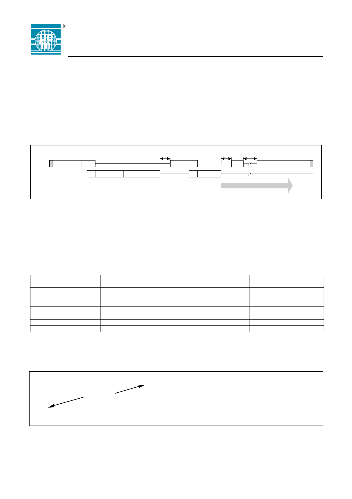
Power-On-Reset (POR)
When the EM4450/4550 with its attached coil enters an electromagnetic field, the built in AC/DC converter will supply the
chip. The DC voltage is monitored and a Reset signal is generated to initialise the logic. The contents of the Control word
and Protection word will be downloaded to enable the functions (INIT). The Power-On-Reset is also provided in order to
make sure that the chip will start issuing correct data. Hysteresis is provided to avoid improper operation at the limit level.
V
DD
V
prh
Reset
t
init
EM4450 A ctive
V
prhys
t
t
Fig. 17
Lock All / Lock Memory Area
The EM4450/4550 can be converted to a Read Only chip or be configured to Read/Write and Read Only Areas by
programming the protection word. This configuration can be locked by write inhibiting the Write Protection Word. Great care
should be taken in doing this operation as there is no further possibility to change the Write Protection Word. The Control
Word can also be protected in the same way thus freezing the operation mode.
Clock Extractor
The Clock extractor will generate a system clock with a frequency corresponding to the frequency of the RF field. The
system clock is used by a sequencer to generate all internal timings.
Data Extractor
The transceiver generated field will be amplitude modulated to transmit data to the EM4450/4550. The Data extractor
demodulates the incoming signal to generate logic levels, and decodes the incoming data.
Modulator
The Data Modulator is driven by the serial data output from the memory which is Manchester encoded. The modulator will
draw a large current from both coil terminals, thus amplitude modulating the RF field according to the memory data.
AC/DC Converter and Voltage Limiter
The AC/DC converter is fully integrated on chip and will extract the power from the incident RF field. The internal DC
voltage will be clamped to avoid high internal DC voltage in strong RF fields.
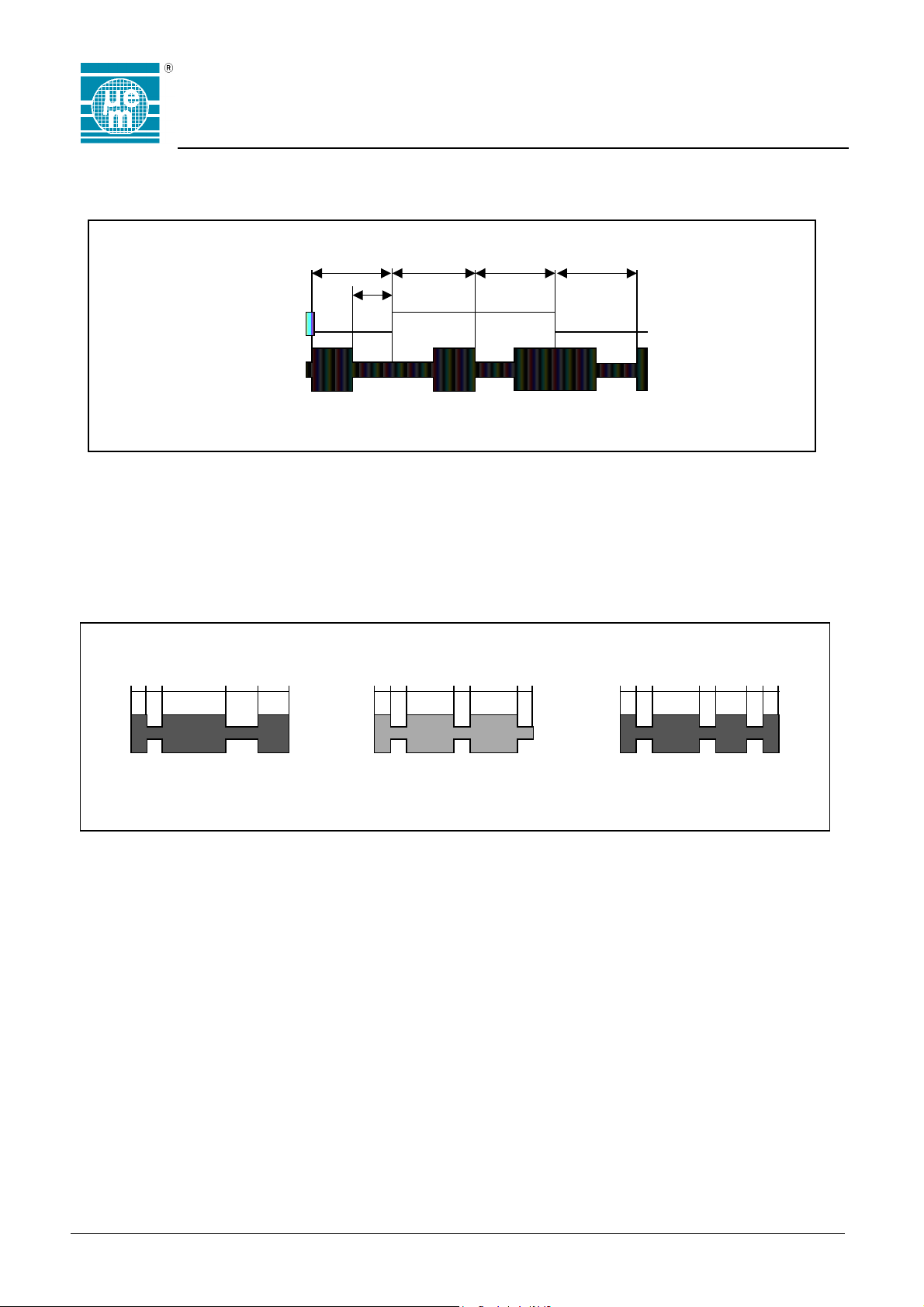
Special Timings
The Processing Pause Time (t
), Write Access Time (twa) and EEPROM Write Time (t
pp
) are timings where the
wee
EM4450/4550 is executing internal operations. During these pauses, the RF field will be influenced.
RF periods :
Same modulati on
as for a normal bi t
Copyright 2003, EM Microelectronic-Marin SA
32 32
16 16
t
pp
(O pt64)
(O pt32)
(O pt64)
64
32
(O pt32)
t
wa
Dur ing Twa and Twee, the si gnal on the coi l is
damped due to a hig her c urrent c onsumption.
3200
2624
t
(O pt64)
(O pt32)
wee
Fig. 18
10 www.emmicroelectronic.com
Page 11
EM4450
EM4550
Communication from Transponder to the Transceiver (READ MODE)
The EM4450/4550 modulates the amplitude of the RF field to transmit data to the transceiver. Data are output serially from
the EEPROM and Manchester encoded.
1 bit
64 periods of RF field (Opt64)
32 periods of RF field (Opt32)
Data from EEPROM
Coded Data Measured on the COIL
The EM4450/4550 uses different patterns to send status information to the transceiver. Their structure can not be confused
with a bit pattern sequence. These patterns are the Listen Window (LIW) to inform the transceiver that data can be
accepted, the Acknowledge (ACK) indicating proper communication and end of EEPROM write, and the No Acknowledge
(NAK) when something is wrong.
The LIW, due to its special structure, can be used to synchronize the transceiver during a read operation. The LIW is sent
before each word, and is sent twice before FWR.
1 bit 1 bit 1 bit
32 periods (Opt64)
16 periods (Opt32)
Opt64 is the chip option with a bit period corresponding to 64 periods of the RF field
Opt32 is the chip option with a bit period corresponding to 32 periods of the RF field
Fig. 19
LIW ACK NAK
32 32 128 64 64 32 32 96 32 64 32 32 32 32 96 32 96 32
All numbers repres ent number of periods of RF f ield
Communication from the Transceiver to the Transponder (RECEIVE MODE)
The EM4450/4550 can be switched to the Receive Mode ONLY DURING A LISTEN WINDOW. The Transceiver is
synchronized with the incoming data from the transponder and expects a LIW before each word. During the phase where
the chip has its modulator "ON" (64/32 periods of RF [Opt64/Opt32] ), the transceiver has to send a bit "0". A certain phase
shift in the read path of the transceiver can be accepted due to the fact that when entering Receive Mode, the Transceiver
becomes the Master.
At reception of the first "0", the chip immediately stops the LIW sequence and then expects another bit "0" to activate the
receive mode. Once the EM4450/4550 has received the first bit "0", the transceiver is imposing the timing for
synchronisation.
The EM4450/4550 turns "ON" its modulator at the beginning of each frame of a bit period. To send a logic "1" bit, the
transceiver continues to send clocks without modulation. After half a bit period, the modulation device of the EM4450/4550
is turned "OFF" allowing recharge of the internal supply capacitor. To send a logic "0" bit, the transceiver stops sending
clocks (100% modulation) during the first half of a bit period. The transceiver must not turn "OFF" the field after 7/4 clocks of
the bit period (Opt64/Opt32). The field is stopped for the remaining first half of the bit period, and then turned "ON" again for
the second half of the bit period. The 32rd/16th clock (Opt64/Opt32) defines the end of the bit.
To ensure synchronisation between the transceiver and the transponder, a logic bit set to "0" has to be transmitted at
regular intervals. The RM pattern consists of two bits set to "0" thus allowing initial synchronisation. In addition, the chosen
data structure contains even parity bits which will not allow more than eight consecutive bits set to logic "1" where no
modulation occurs.
(Opt64)
(Opt32)
(Opt64)
(Opt32)
Opt6 4 is th e chi p opti on with a bi t per io d cor respo ndi ng t o 64 per iods of th e RF fiel d
Opt3 2 is th e chi p opti on with a bi t per io d cor respo ndi ng t o 32 per iods of th e RF fiel d
16 16 48 16 32 16 16 16 16 48 16 48 16 16 16 64 32 32
(Opt64)
(Opt32)
Fig. 20
Copyright 2003, EM Microelectronic-Marin SA
11 www.emmicroelectronic.com
Page 12
EM4450
EM4550
While the transceiver is sending data to the transponder, two different modulations will be observed on both coils. During
the first half of the bit period, the EM4450/4550 is switching "ON" its modulation device causing a modulation of the RF field.
This modulation can also be observed on the transceiver's coil. The transceiver sending a bit "0" will switch "OFF" the field,
causing a 100% modulation being observed on the transponder coil.
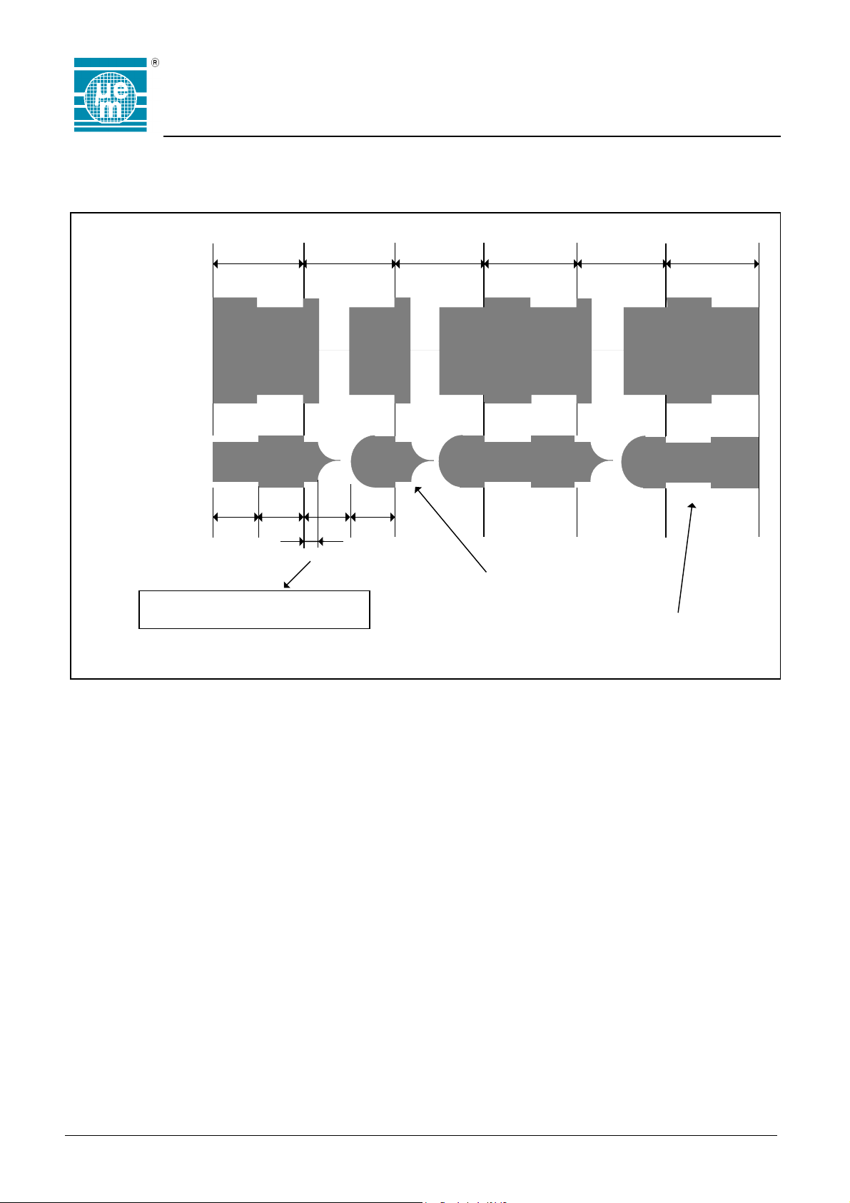
Bit Period
DATA :
Transceiver
Coil
Transponder
Coil
"1" "1" "1""0" "0" "0"
Periods of RF field (Opt 64):
Periods of RF field (Opt 32):
Recommended
*
Minimum
32 32 32 32
16 16
16
*
: 7/4 periods (Opt64/Opt32)
: 1 period
Opt64 is the chip option with a bit period corresponding to 64 priods of the RF field
Opt32 is the chip option with a bit period corresponding to 32 priods of the RF field
16
Modulation induced by the Transceiver
Modulation induced by the Transponder
Fig. 21
Copyright 2003, EM Microelectronic-Marin SA
12 www.emmicroelectronic.com
Page 13

Package Information
Dimensions of PCB and CID version
EM4450
EM4550
CID Package
FRONT V IEW
JK
SYMBOL MIN TYP MAX
A 8.2 8.5 8.8
B 3.8 4.0 4.2
D 5.8 6.0 6.2
e 0.38 0.5 0.62
F 1.25 1.3 1.35
g 0.3 0.4 0.5
J 0.42 0.44 0.46
A
K 0.115 0.127 0.139
R 0.4 0.5 0.6
Dimensions are in mm
D
TOP VIEW
B
MARKING
AREA
R
C1
C2
FF
g
e
PCB Packa ge
Y
X
Z
C2 C1
SYMBOL MIN TYP MAX
X8.0
Y4.0
Z1.0
Dimensions are in mm
Fig. 22 Fig. 23
Copyright 2003, EM Microelectronic-Marin SA
13 www.emmicroelectronic.com
Page 14

EM4450
EM4550
Chip Dimensions
1511
1112
Y
X
Pad size : 86 X 86
200
10
174
895
740
585
430
280
140
114
167
8
EM4550
3
903
714
189
1237
2345678
130
270
420
575
730
885
9
EM4450
889
1237
1
1824
1425
200
Y
X
234567
19
Pad size : 86 X 86
All dimensions in µm
Mega pad size : 200 X 400
All dimensions in µm
Fig. 24 Fig. 25
Pad Description
Pad Name Function
1 COIL1 Coil Terminal 1
2 TEST_CLK Test Clock input with pull-down
3 TEST_IN Test Input with pull-down
4 TEST Test Mode Input with pull-down
5 TEST_OUT Test Output
6 VDD Positive Internal Supply Voltage
7 VPOS Internal Supply
8 VSS Negative Internal Supply Voltage
9 COIL2 Coil Terminal 2
Copyright 2003, EM Microelectronic-Marin SA
14 www.emmicroelectronic.com
Page 15

EM4450
ga p
V
y)
y)
r
)
)
)
)
V
p
g p
g
EM4550
Ordering Information
Die Form
This chart shows general offering; for detailed Part Number to order, please see the table “Standard Versions” below.
EM4450 A6 WS 11 %%%
Circuit Nb: Customer Version:
EM4450: standard pads %%% = only for custom specific version
EM4550: me
ersion: Bumping:
A6 = Manchester, 64 clocks per bit " " (blank) = no bumps (EM4450 onl
A5 = Manchester, 32 clocks per bit E = with Gold Bumps (EM4550 onl
Die form: Thickness:
WW = Wafe
WS = Sawn Wafer/Frame 7 = 7 mils (178um
WT = Sticky Tape 11 = 11 mils (280um
ads
-
6 = 6 mils (152um
27 = 27 mils (686um
Packaged Devices
This chart shows general offering; for detailed Part Number to order, please see the table “Standard Versions” below.
CI2LC %%%EM4450 A6
Circuit Nb: Customer Version:
EM4450: standard pads %%% = only for custom specific version
ersion:
A6 = Manchester, 64 clocks per bit
A5 = Manchester, 32 clocks
Package/Card & Delivery Form:
CI2LB = CID Pack, 2 long pins (2.5mm), in tape
CI2LC = CID Pack, 2 lon
CB2RC = PCB Packa
er bit
ins (2.5mm), in bulk
e, 2 pins, in bulk
-
Remarks:
• For ordering please use table of “Standard Version” table below.
• For specifications of Delivery Form, including gold bumps, tape and bulk, as well as possible other delivery form or
packages, please contact EM Microelectronic-Marin S.A.
Copyright 2003, EM Microelectronic-Marin SA
15 www.emmicroelectronic.com
Page 16

Standard Versions & Samples:
For samples please order exclusively:
EM4450
EM4550
Part Number Bit coding
EM4450 A6 CI2LC Manchester 64 Standard CID package, 2 pins (length 2.5mm) bulk
EM4450 A6 CB2RC Manchester 64 Standard PCB Package, 2 pins bulk
The versions below are considered standards and should be readily available. For other versions or other delivery form,
please contact EM Microelectronic-Marin S.A. Please make sure to give complete part number when ordering, without
spaces between characters.
Part Number Bit coding
EM4450 A5 CB2RC Manchester 32 Standard PCB Package, 2 pins bulk
EM4450 A5 CI2LC Manchester 32 Standard CID package, 2 pins (length 2.5mm) bulk
EM4450 A6 CB2RC Manchester 64 Standard PCB Package, 2 pins bulk
EM4450 A6 CI2LB Manchester 64 Standard CID package, 2 pins (length 2.5mm) tape
EM4450 A6 CI2LC Manchester 64 Standard CID package, 2 pins (length 2.5mm) bulk
EM4450 XX YYY-%%% Manchester 32/64 Standard custom custom
EM4550 A6 WS11E Manchester 64 Mega Sawn wafer, 11 mils with gold bumps
EM4550 A6 WT11E Manchester 64 Mega Die on sticky tape, 11 mils with gold bumps
EM4550 XX YYY-%%% Manchester 32/64 Mega custom with gold bumps
Cycle/
bit
Cycle/
bit
Pads Package
Pads Package/Die Form Delivery Form
Delivery
Form
/ Bumping
Product Support
Check our Web Site under Products/RF Identification section.
Questions can be sent to cid@emmicroelectronic.com
EM Microelectronic-Marin SA cannot assume responsibility for use of any circuitry described other than circuitry entirely embodied in an EM
Microelectronic-Marin SA product. EM Microelectronic-Marin SA reserves the right to change the circuitry and specifications without notice
at any time. You are strongly urged to ensure that the information given has not been superseded by a more up-to-date version.
© EM Microelectronic-Marin SA, 01/03,Rev.B
Copyright 2003, EM Microelectronic-Marin SA
16 www.emmicroelectronic.com
 Loading...