

Page 1
Etr onT ech
EM566168
1M x 16 Pseudo SRAM
Preliminary, Rev 0.2 Apr. 2002
Features
Organized as 1M words by 16 bits
•
Fast Cycle Time : 70ns
•
Standby Current : 100uA
•
Deep power-down Current : 10uA (Memory cell data
•
invalid)
Byte data control: LB# (DQ0 - 7), UB# (DQ8 - 15)
•
Compatible with low power SRAM
•
Single Power Supply Voltage : 3.0V±0.3V
•
Package Type : 48-ball FBGA, 6x8mm
•
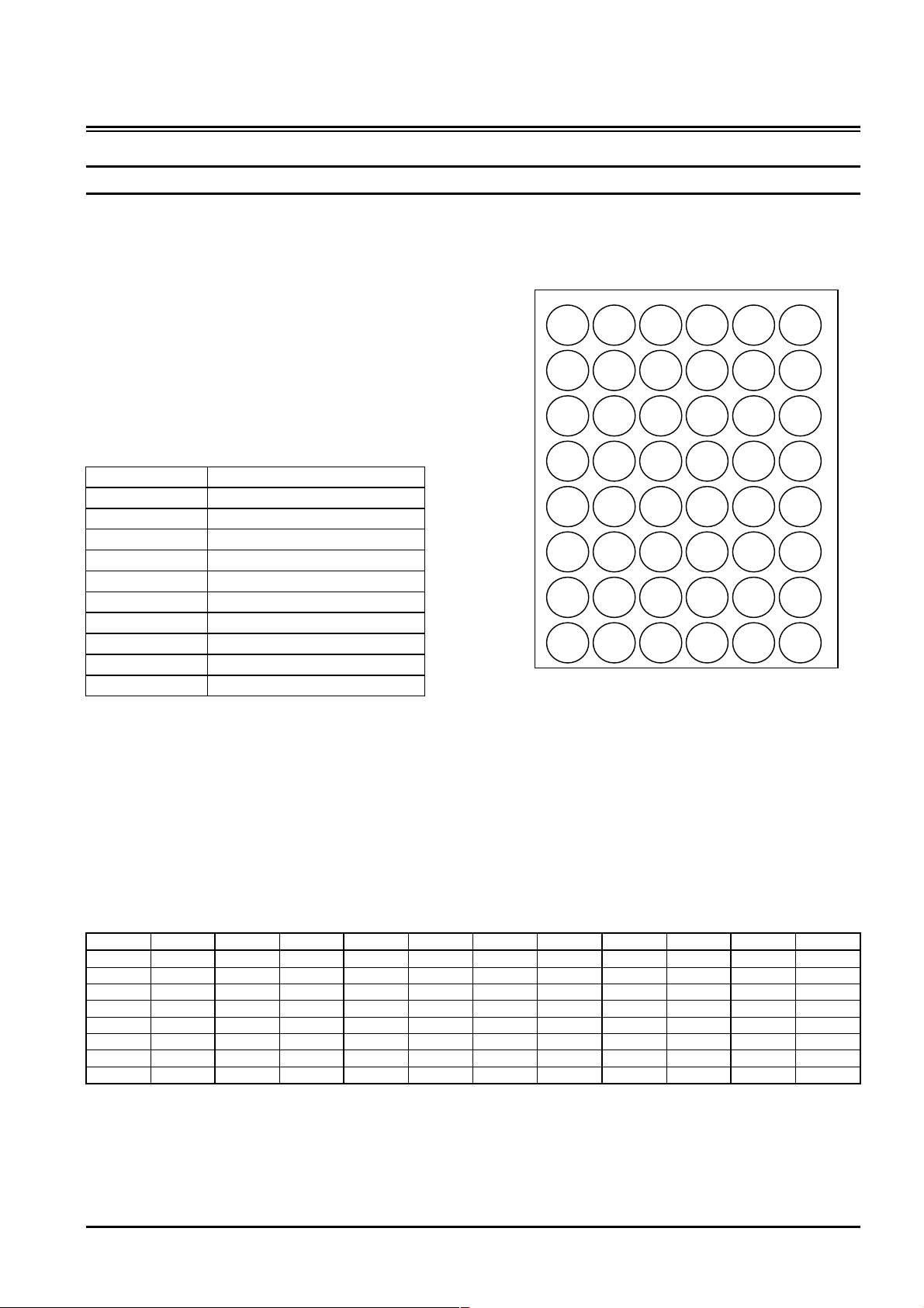
Pin Description
Symbol
A0 – A19 Address Inputs
DQ0 – DQ15 Data Inputs/Outputs
CE1# Chip Enable
CE2 Deep Power Down
OE# Output Enable
WE# Write Control
LB# Lower Byte Control
UB# Upper Byte Control
VCC Power Supply
VSS Ground
Function
Pin Assignment 48-Ball BGA, Top View
6 5 4 3 2 1
A
B
C
D
E
F
G
H
LB# OE#
DQ8 UB#
DQ9 DQ10
VSS DQ11
VCC DQ12
DQ14 DQ13
DQ15 A19
A18 A8
A0 A1
A3 A4
A5 A6
A17 A7
NC A16
A14 A15
A12 A13
A9 A10
A2 CE2
CE1# DQ0
DQ1 DQ2
DQ3 VCC
DQ4 VSS
DQ5 DQ6
WE# DQ7
A11 NC
Overview
The EM566168 is a 16M-bit Pseudo SRAM organized as 1M words by 16 bits. It is designed with advanced
CMOS technology specified RAM featuring low power static RAM compatible function and pin configuration. This
device operates from a single power supply. Advanced circuit technology provides both high speed and low
power. It is automatically placed in low-power mode when CS1# or both UB# and LB# are asserted high or CS2
is asserted low. There are three control inputs. CS1# and CS2 are used to select the device, and output enable
(OE#) provides fast mem ory access. Data byte control pins (LB#,UB#) provide lower and upper byte access .
This device is well suited to various microprocessor system applications where high speed, low power and
battery backup are required. And, with a guaranteed wide operating range, the EM566168 can be used in
environments exhibiting extreme temperature conditions.
Pin Location
Symbol Location Symbol Location Symbol Location Symbol Location Symbol Location Symbol Location
A0 A3 A8 H2 A16 E4 DQ3 D5 DQ11 D2 WE# G5
A1 A4 A9 H3 A17 D3 DQ4 E5 DQ12 E2 LB# A1
A2 A5 A10 H4 A18 H1 DQ5 F5 DQ13 F2 UB# B2
A3 B3 A11 H5 A19 G2 DQ6 F6 DQ14 F1 VCC D6
A4 B4 A12 G3 NC H6 DQ7 G6 DQ15 G1 VCC E1
A5 C3 A13 G4 DQ0 B6 DQ8 B1 CE1# B5 GND D1
A6 C4 A14 F3 DQ1 C5 DQ9 C1 CE2 A6 GND E6
A7 D4 A15 F4 DQ2 C6 DQ10 C2 OE# A2 NC E3
Etron Technology, Inc.
No. 6, Technology Rd. V, Science-Based Industrial Park, Hsinchu, Taiwan 30077, R.O.C.
TEL: (886)-3-5782345 FAX: (886)-3-5778671
Etron Technology, Inc., reserves the right to make changes to its products and specifications without notice.
Page 2
Etr onT ech
R
C
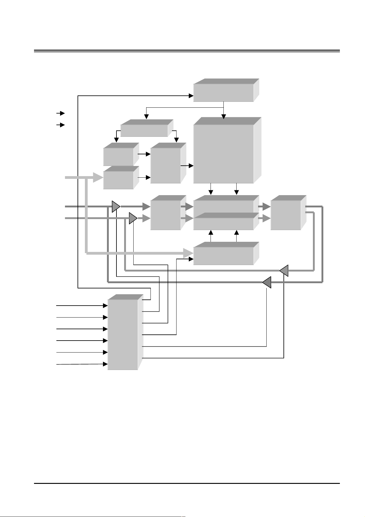
Block Diagram
VCC
EM566168
Standby/Deep Power
Down Mode Control
VSS
A0 – A19
DQ0 – DQ7
DQ8 – DQ15
efresh
ounter
Address
Buffer
Refresh Control
Address
Decoder
Control
Row
Input
Data
Memory Cell Array
1M x 16
Sense AMP
Column Decoder
Address Buffer
Output
Data
Control
CS1#
CS2
OE#
WE#
LB#
UB#
Control
Logic
Preliminary 2 Rev 0.2
Feb. 2002
Page 3
Etr onT ech
EM566168
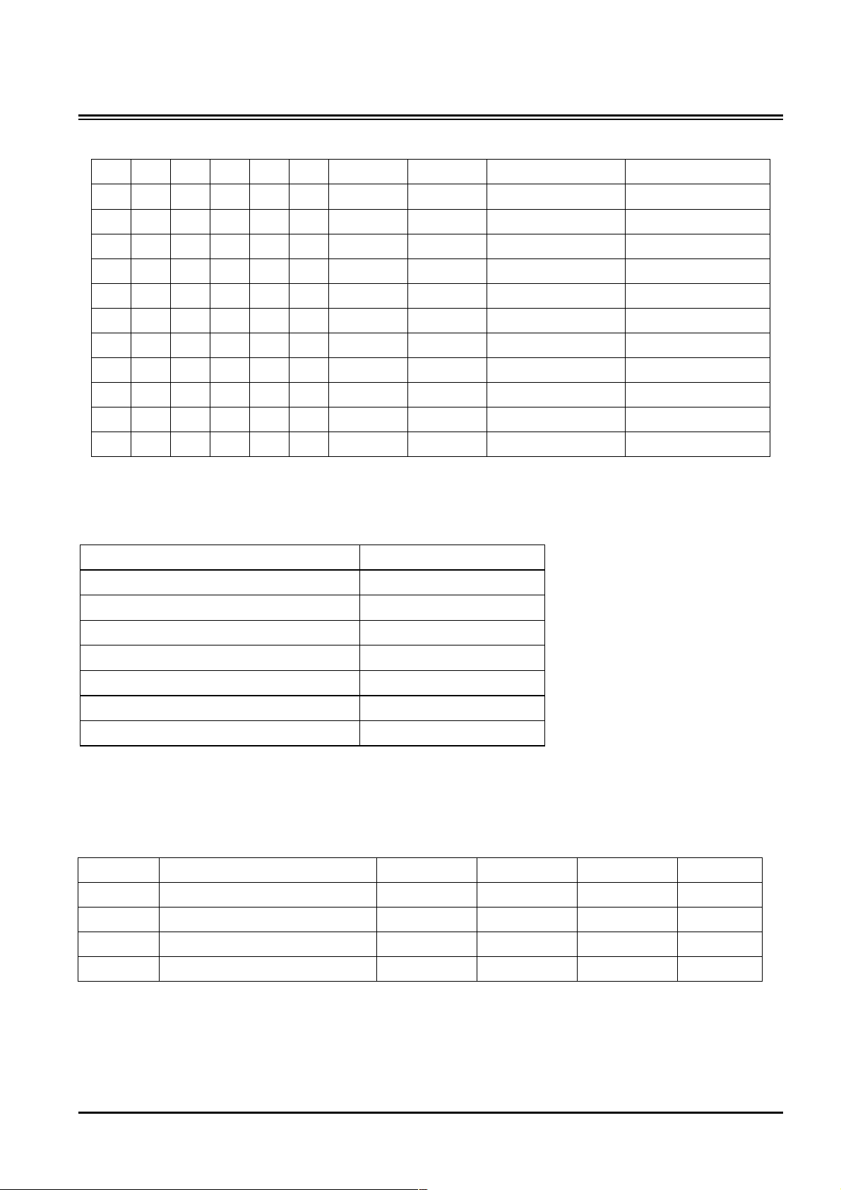
Operating Mode
CS1# CS2 OE# WE# LB# UB# DQ0~DQ7 DQ8~DQ15 Mode Power
H H X X X X High-Z High-Z Deselect Standby
X L X X X X High-Z High-Z Deselect Deep Power Down
L H X X H H High-Z High-Z Deselect Standby
L H H H L X High-Z High-Z Output Disabled Active
L H H H X L High-Z High-Z Output Disabled Active
L H L H L H D-out High-Z Lower Byte Read Active
L H L H H L High-Z D-out Upper Byte Read Active
L H L H L L D-out D-out Word Read Active
L H X L L H D-in High-Z Lower Byte Write Active
L H X L H L High-Z D-in Upper Byte Write Active
L H X L L L D-in D-in Word Write Active
Note:
X=don’t care. H=logic high. L=logic low.
Absolute Maximum Ratings1)
Supply voltage, VCC -0.2 to +3.6V
Input voltages, VIN -0.2 to VCC + 0.3V
Input and output voltages, VIN, V
Output short circuit current ISH 100 mA
Operating temperature, TA
Storage temperature, T
Soldering Temperature (10s), T
Power dissipation, PD 1 W
Note:
Absolute maximum DC requirements contains stress ratings only. Functional operation at the absolute
maximum limits is not implied or guaranteed. Extended exposure to maximum ratings may affect device
reliability.
STRG
-2.0 to +3.6V*
OUT
-25 to +85°C
-65 to +125°C
SOLDER
240°C
Recommended DC Operating Conditions
Symbol Parameter Min. Typ. Max. Unit
VCC Power Supply Voltage 2.7 3.0 3.3 V
VSS Ground 0
−
0 V
VIH Input High Voltage 2.2
VIL Input Low Voltage -0.22)
Notes:
1. Overshoot: VCC + 2.0V in case of pulse width ≤ 20ns
2. Undershoot: -2.0V in case of pulse width ≤ 20ns
3. Overshoot and undershoot are sampled, not 100% tested.
−
−
VCC+0.21) V
Preliminary 3 Rev 0.2
+0.6 V
Feb. 2002
Page 4
Etr onT ech
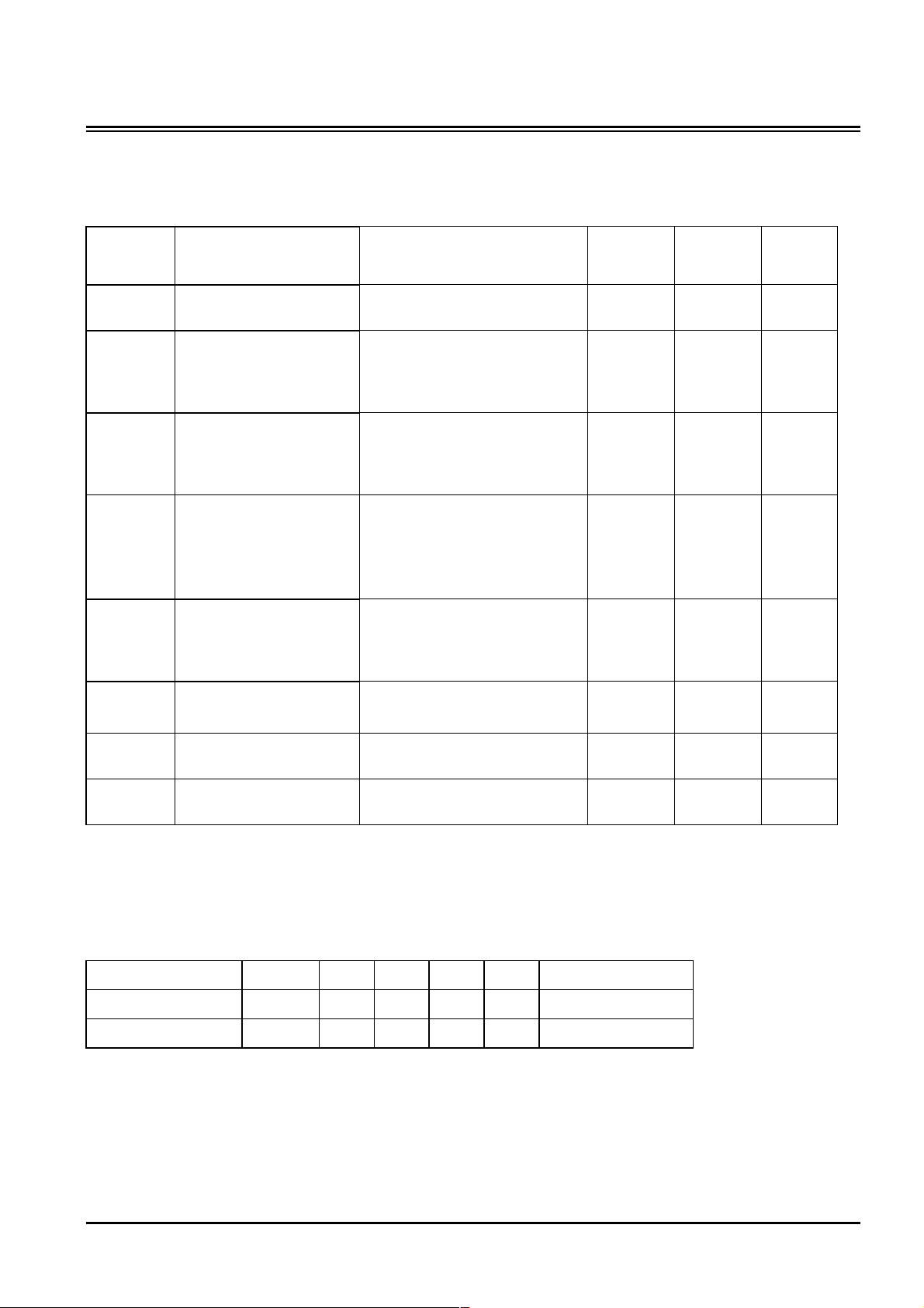
DC Characteristics
EM566168
Symbol
ILI
ILO
Input Leakage Current
Output Leakage Current
Parameter Test Conditions Min. Max. Unit
Operating Current @ Min
I
CC1
Cycle Time
Operating Current @ Max
I
CC2
I
SB1
I
SBD Deep Power Down
Cycle Time (1µs)
Standby Current (CMOS)
VIN = VSS to VDD
VIO = VSS to VDD
CE1# = VIH, CE2 = VIL or
OE# = V
or WE# = VIL
IH
Cycle time = Min., 100% duty
IIO = 0mA, CE1# = VIL,
CE2 = VIH, V
IN
= V
IH
or VIL
Cycle time = 1µs, 100% duty
IIO = 0mA, CE1# ≤ 0.2V,
CE2 ≥ V
IN
≥
or V
CE1# = V
CE2 = V
DD
V
DD
DD
-0.2V, V
DD
– 0.2V,
-0.2V
– 0.2V and
IN
≤
0.2V
Other inputs = VSS ~ VCC
≤
CE2
0.2V, Other inputs =
VSS ~ VCC
-1 1
-1 1
−
−
−
25 mA
3 mA
100
10
µ
A
µ
A
µ
A
µ
A
VOL
VOH
Output Low Voltage IOL = 2.1mA
−
Output High Voltage IOH = -1.0mA 2.4
0.4
Capacitance (Ta = 25°C; f = 1 MHz)
Parameter Symbol Min Typ Max Unit Test Conditions
Input capacitance CIN
Output capacitance C
Notes:
These parameters are sampled and not 100% tested.
OUT
−
−
−
−
8 pF VIN = GND
10 pF V
OUT
= GND
V
−
V
Preliminary 4 Rev 0.2
Feb. 2002
Page 5
Etr onT ech
EM566168
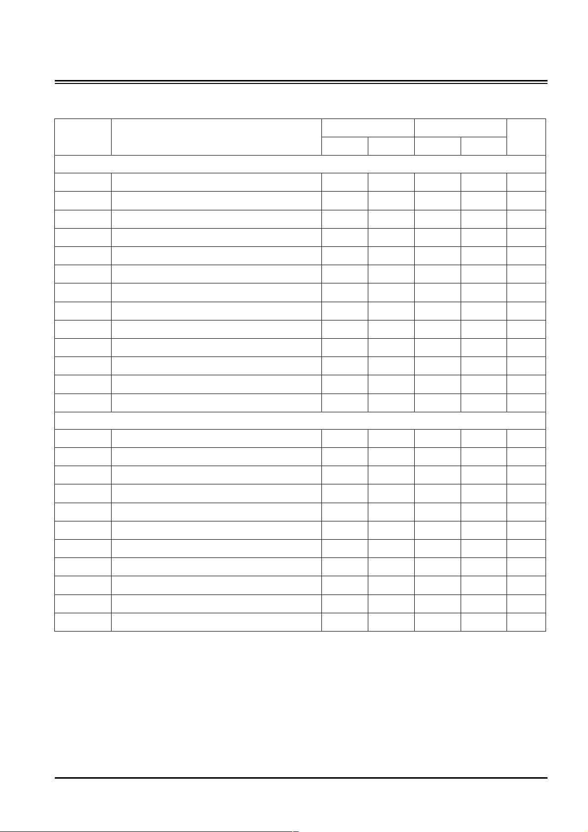
AC Characteristics and Operating Conditions (Ta = -25°C to 85°C, VCC = 2.7V to 3.3V)
Symbol
tRC Read cycle time
tAA Address access time
t
Chip Enable (CE1#) Access Time
CO1
t
Chip Enable (CE2) Access Time
CO2
tOE Output enable access time
tBA Data Byte Control Access Time
tLZ Chip Enable Low to Output in Low-Z
t
Output enable Low to Output in Low-Z
OLZ
t
Data Byte Control Low to Output in Low-Z
BLZ
tHZ Chip Enable High to Output in High-Z
t
Output Enable High to Output in High-Z
OHZ
t
Data Byte Control High to Output in High-Z
BHZ
tOH Output Data Hold Time
Parameter
Read Cycle
-85 -70
Min Max Min Max
85
−
−
−
−
−
10
5
10
−
−
−
10
−
85
85
85
40
85
−
−
−
35
35
35
−
70
−
−
−
−
−
10
5
10
−
−
−
10
−
70 ns
70 ns
70 ns
35 ns
70 ns
−
−
−
25 ns
25 ns
25 ns
−
Unit
ns
ns
ns
ns
ns
tWC Write Cycle Time
tWP Write Pulse Width
tAW Address Valid to End of Write
tCW Chip Enable to End of Write
tBW Data Byte Control to End of Write
tAS Address Setup Ttime
tWR Write Recovery Ti me
t
WE# Low to Output in High-Z
WHZ
tOW WE# High to Output in Low-Z
tDW Data to Write Overlap
tDH Data Hold Time
AC Test Condition
Output load : 50pF + one TTL gate
•
Input pulse level : 0.4V, 2.4
•
Timing measurements : 0.5 x VCC
•
tR, tF : 5ns
•
Write Cycle
85
60
70
70
70
0
0
−
5
30
0
−
−
−
−
−
−
−
30
−
−
−
70
50
60
60
60
0
0
−
5
30
0
−
−
−
−
−
−
−
20 ns
−
−
−
ns
ns
ns
ns
ns
ns
ns
ns
ns
ns
Preliminary 5 Rev 0.2
Feb. 2002
Page 6
Etr onT ech
C
R
C
C
C
C
o
C
U
I
(
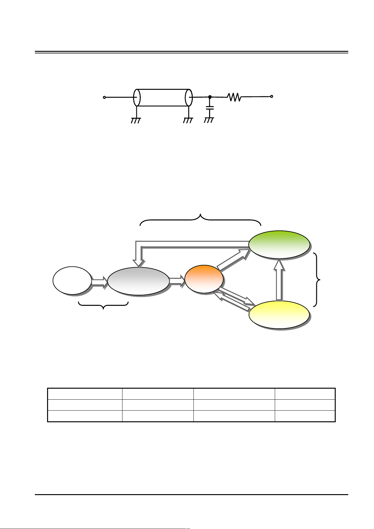
AC Test Loads
Note:
1. Including scope and jig capacitance
State Diagram
Power
Standby Mode Characteristics
D
OUT
CE1# =VIH or
VIL, CE2=VIH
nitial State
on
Wait 200µs)
Power Up Sequence
Z0 = 50 Ω
Deep Power Dow n Exi t
E1# = VIH or VIL,
E2=VIH
Active
E1# =VIL, CE2=VIH,
B# & LB# or/and LB# = VIL
= 50 Ω
L
1
= 50 pF
L
Sequence
E2=VIL
E2=VIH, CE1# =VIH
r UB#, LB# =VIH
EM566168
VL = 1.5 V
Deep Power
Down Mode
CE2=VIL
Standby
Mode
Power Mode Memory Cell Data St andby Current (µA) Wait Time (µs)
Standby Valid 100 0
Deep Power Down Invalid 10 200
Preliminary 6 Rev 0.2
Feb. 2002
Page 7
Etr onT ech
t
t
P
D
t
t
t
t
t
t
t
t
t
H
H
D
t
t
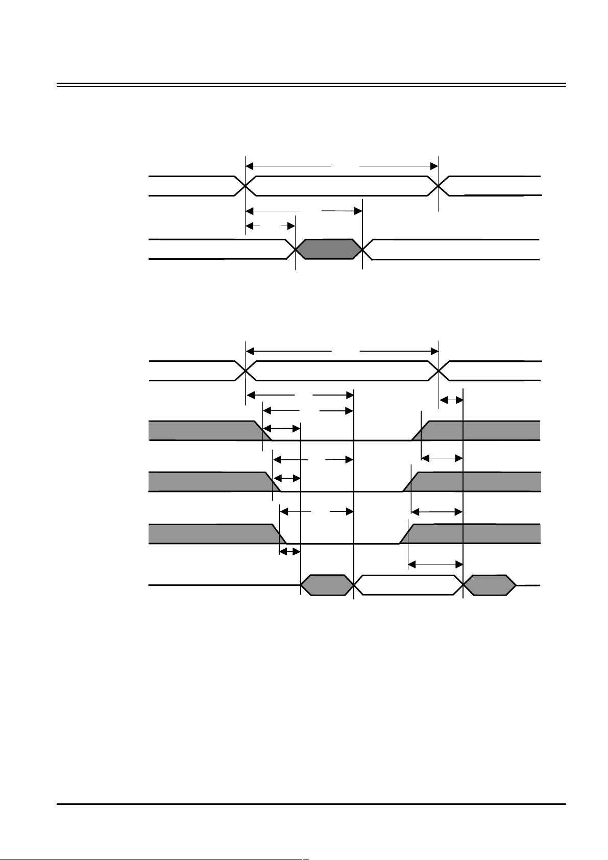
Timing Diagrams
Read Cycle 1 – Addressed Controlled
Address
Data Out
revious Data Valid
tOH
EM566168
1)
RC
AA
OH
ata Valid
Read Cycle 2 – CS1# Controlled
Address
CE1#
UB#, LB#
OE#
Data Out
igh-Z
Notes:
2)
LZ
BLZ
OLZ
AA
CO
RC
tOH
tHZ
BA
BHZ
OE
OHZ
igh-Z
ata Valid
1. CE1# = OE# = V
2. CE2 = WE# = V
, CE2 = WE# = VIH, UB# or/and LB# = VIL
IL
IH
Preliminary 7 Rev 0.2
Feb. 2002
Page 8
Etr onT ech
t
t
t
t
t
H
D
t
t
t
t
t
t
t
t
D
t
t
t
t
EM566168
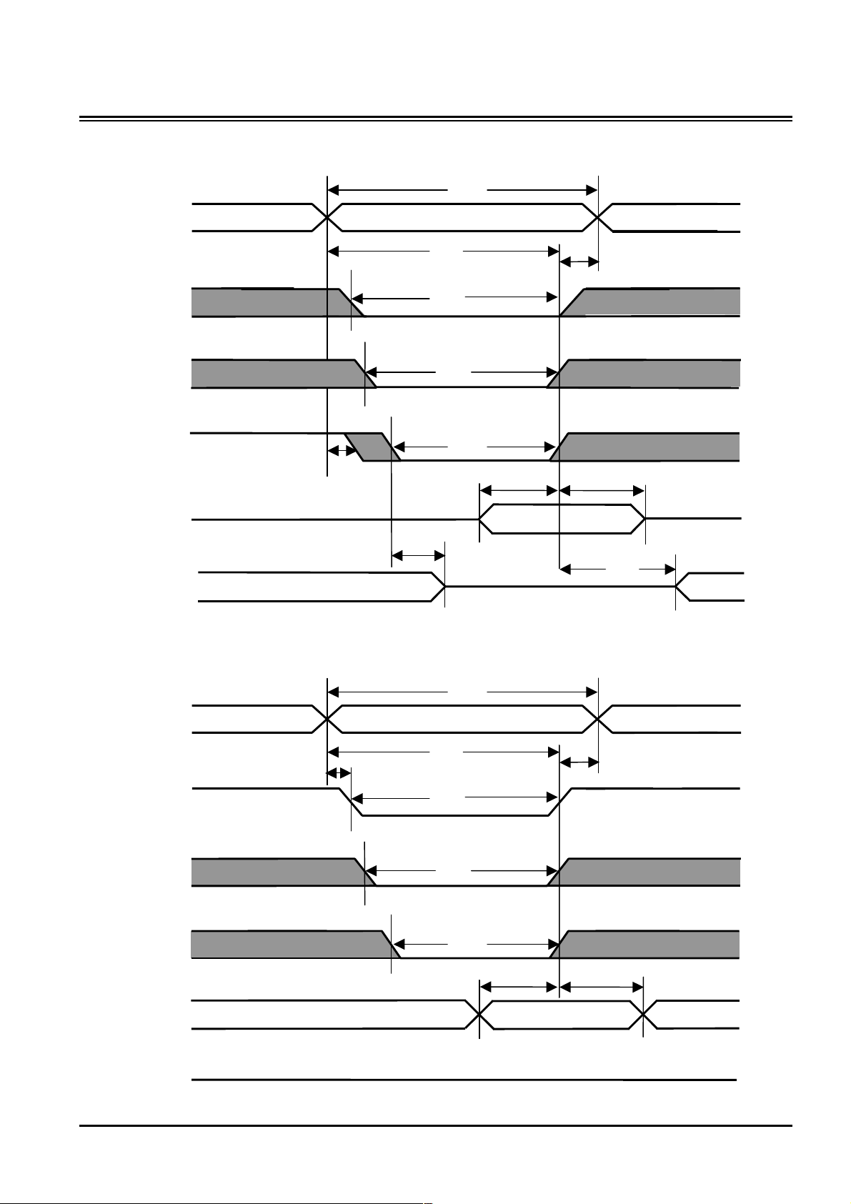
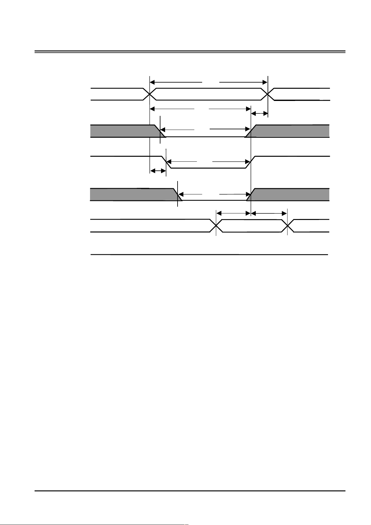
Write Cycle 1 – WE# Controlled
Address
CE1#
UB#, LB#
WE#
Data In
Data Out
igh-Z
Data Undefined
Write Cycle 2 – CS1# Controlled
1) 2)
tAS
1) 2)
WC
AW
WR
CW
BW
WP
DW
DH
High-Z
ata Valid
WHZ
tOW
Address
CE1#
UB#, LB#
WE#
Data In
Data Out
High-Z
tAS
AW
CW
BW
WC
WP
DW
WR
DH
ata Valid
Preliminary 8 Rev 0.2
Feb. 2002
Page 9
Etr onT ech
t
t
t
t
t
D
t
t
H
EM566168
Write Cycle 3 – UB#, LB# Controlled
Address
CE1#
UB#, LB#
WE#
Data In
Data Out
Notes:
igh-Z
tAS
1) 2)
WC
AW
CW
BW
WP
DW
ata Valid
WR
tDH
1. CE2 = V
IH
2. CE2 = WE# = V
IH
Preliminary 9 Rev 0.2
Feb. 2002
Page 10
Etr onT ech
2
W
R
S
D
D
3
R
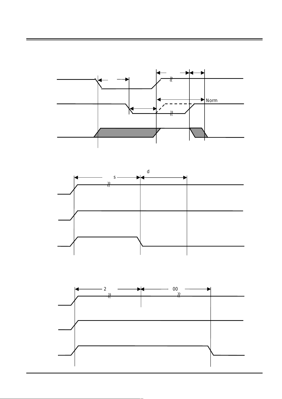
Deep Power Down Mode
CE2
Mode
Normal Operation
CE1#
Power Up 1
V
CC
CE2
CE1#
Power Up 2 (No Dummy Cycle)
Suspend
200µs
a
a
1µs
eep Power
own Mode
ead Operation Tiwce
00µs
a
a
ake Up
a
a
EM566168
ead Operation Twice or
tay High during 300µs
Normal Operation
V
CC
CE2
CE1#
200µs
a
a
00µs
a
a
Preliminary 10 Rev 0.2
Feb. 2002
Page 11
Etr onT ech
<
EM566168
Avoid Timing
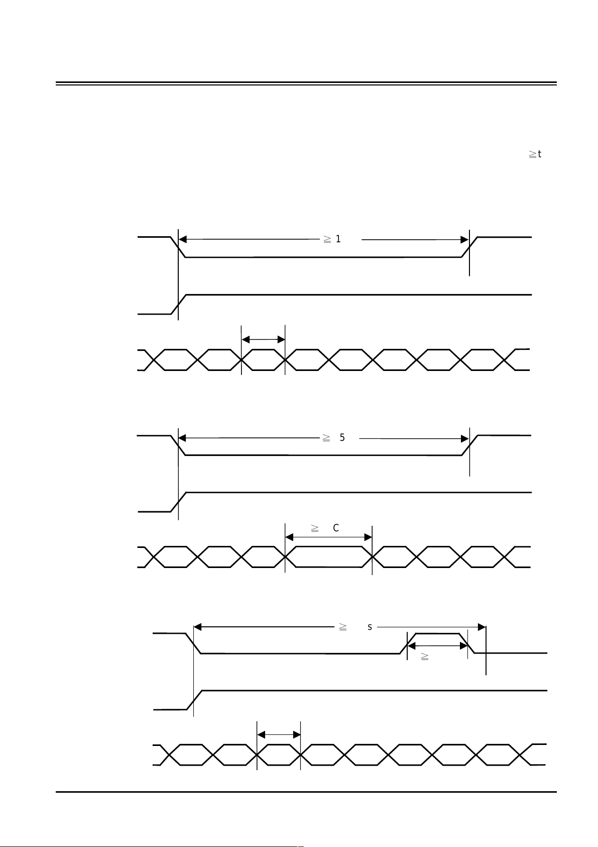
Etron Pseudo SRAM has a timing which is not suppor ted at read oper ation. If your system has m ultiple
invalid address signal shorter than tRC during over 15µs at read operation shown as in Abnormal Timing, it
requires a normal read timing at leat during 15 µs shown as in Avoidable timing 1 or toggle CE1# to high (
one time at least shown as in Avoidable Timing 2.
tRC)
Abnormal Timing
CE1#
WE#
Address
Avoidable Timing 1
CE1#
WE#
Address
Avoidable Timing 2
CE1#
WE#
< tRC
15µs
tRC
15µs
15µs
tRC
tRC
Address
Preliminary 11 Rev 0.2
Feb. 2002
Page 12
Etr onT ech
6
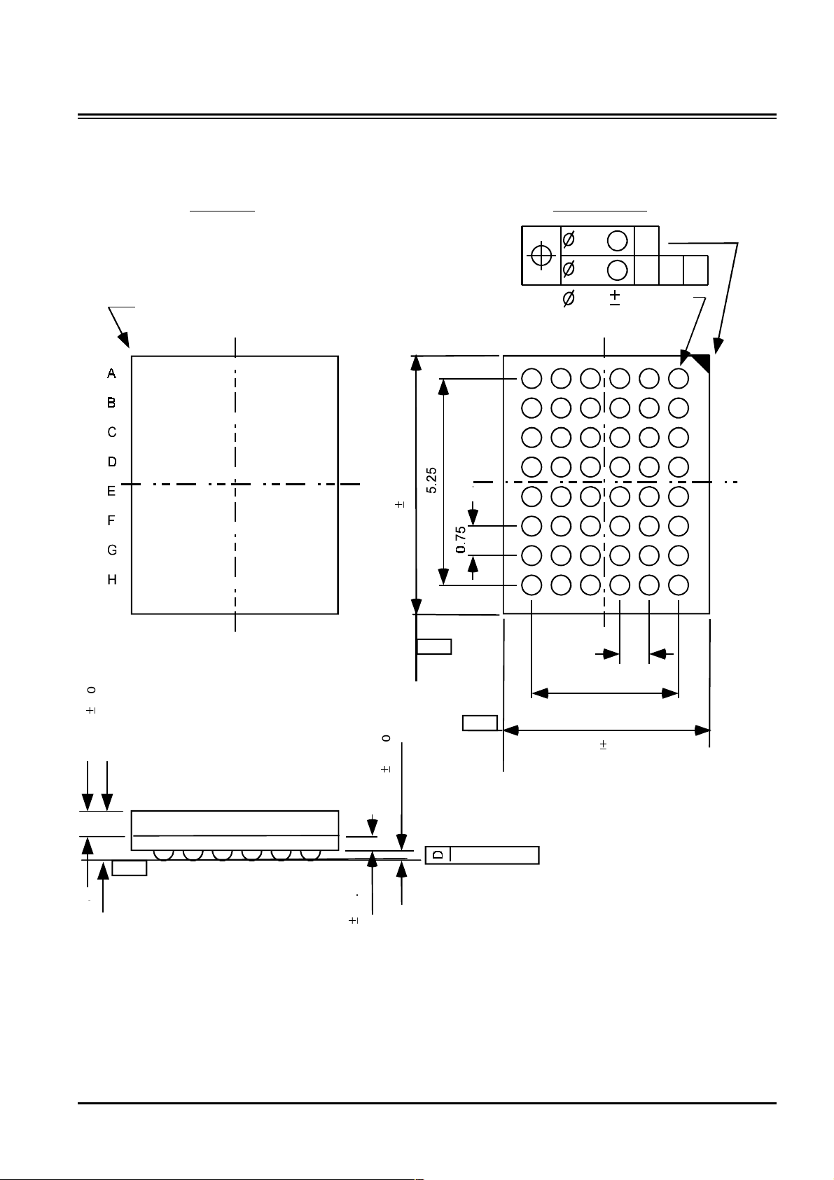
Package Diagrams
48-Ball BGA
Units in mm
TOP VIEW
EM566168
BO TTOM VIEW
PIN 1 CO RN ER
123456
0.1
²
8.0
0.075
S
0.15
S
0.30 0.05(48X)
654321
PIN 1 CO RN ER
C
CAB
0.02
²
0.52
- C - SE ATING PL ANE
5
1
0.
1.20 MAX
5
0
0.
0.04
²
0.32
0.03
²
0.23
- B -
0.75
3.75
- A -
.0 ² 0.1
0.12M AX
Preliminary 12 Rev 0.2
Feb. 2002
 Loading...