

Page 1
10-BIT 5 MSPS A/D CONVERTER
10-BIT 5 MSPS A/D CONVERTER
GENERAL DESCRIPTION
EM19110 is a 10-bit, 5 MHZ CMOS A/D converter for high speed and high resolution use. The 2-step parallel
structures accompanying with an average technique that external generated reference voltage, the users can tune
transfer curve to meet their application.
FEATURES
• 5 MSPS maximum conversion speed
• High resolution up to 10 bit
• Built-in sampling and hold circuit
• Internal self-bias reference voltage
• 115 mW low power dissipation at 5MSPS
• +5V single power supply
• Available in 24 pin SOP
• Series
EM19110M for 300 mil SOP
EM19110
EM19110
APPLICATION
Precision scanner, digital cellular phone and a wide range of fields where high speed and high resolution A/D
conversion is required in the digital communication.
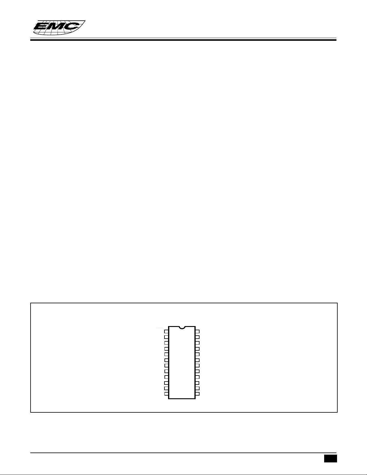
PIN ASSIGNMENT
EM19110
OE
D0(LSB)
D1
D2
D3
D4
D5
D6
D7
D8
D9(MSB)
CLK
1
2
3
4
5
6
7
8
9
10
11
12
DVSS
24
VRB
23
VRBS
22
AR1
21
AVSS
20
VIN
19
AVDD
18
VR2
17
VR3
16
VRT
15
VRTS
14
DVDD
13
* This specification are subject to be changed without notice.
5.26.1997
1
Page 2
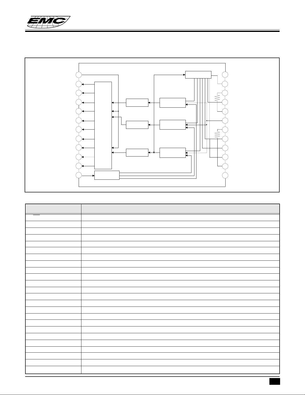
FUNCTIONAL BLOCK DIAGRAM
EM19110
10-BIT 5 MSPS A/D CONVERTER
1
/OE
D0
2
D1
3
D2
4
D3
5
D4
6
D5
7
D6
8
D7
9
D8
10
D9
11
12
CLK DVDD
Error
correction
and
data
latches
Clock center
Fine encoder
Fine encoder
Coarse encoder
Fine
Comparators with
S/ H (6bit)
Fine
Comparators with
S/ H (6bit)
Coarse
Comparators with
S/ H (4bit)
PIN DESCRIPTIONS
Symbol Function
OE Output enable
D0 Data output bit 0 (LSB)
D1 Data output bit 1
D2 Data output bit 2
D3 Data output bit 3
D4 Data output bit 4
D5 Data output bit 5
D6 Data output bit 6
D7 Data output bit 7
D8 Data output bit 8
D9 Data output bit 9 (MSB)
CLK Clock input
DVDD Digital power supply
VRTS Top internal reference voltage
VRT Top reference voltaget
VR3 Tap-3 reference voltage
VR2 Tap-2 reference voltage
AVDD Analog power supply
VIN Analog input voltage
AVSS Analog ground
VR-1 Tap-1 reference voltage
VRBS Bottom internal reference voltage
VRB Bottom reference voltage
DVSS Digital ground
Ladder resistors
DVSS
24
VRB
23
VRBS
22
21
VR1
20
AVSS
VIN
19
AVDD
18
17
VR2
VR3
16
VRT
15
14
VRTS
13
* This specification are subject to be changed without notice.
5.26.1997
2
Page 3
EM19110
10-BIT 5 MSPS A/D CONVERTER
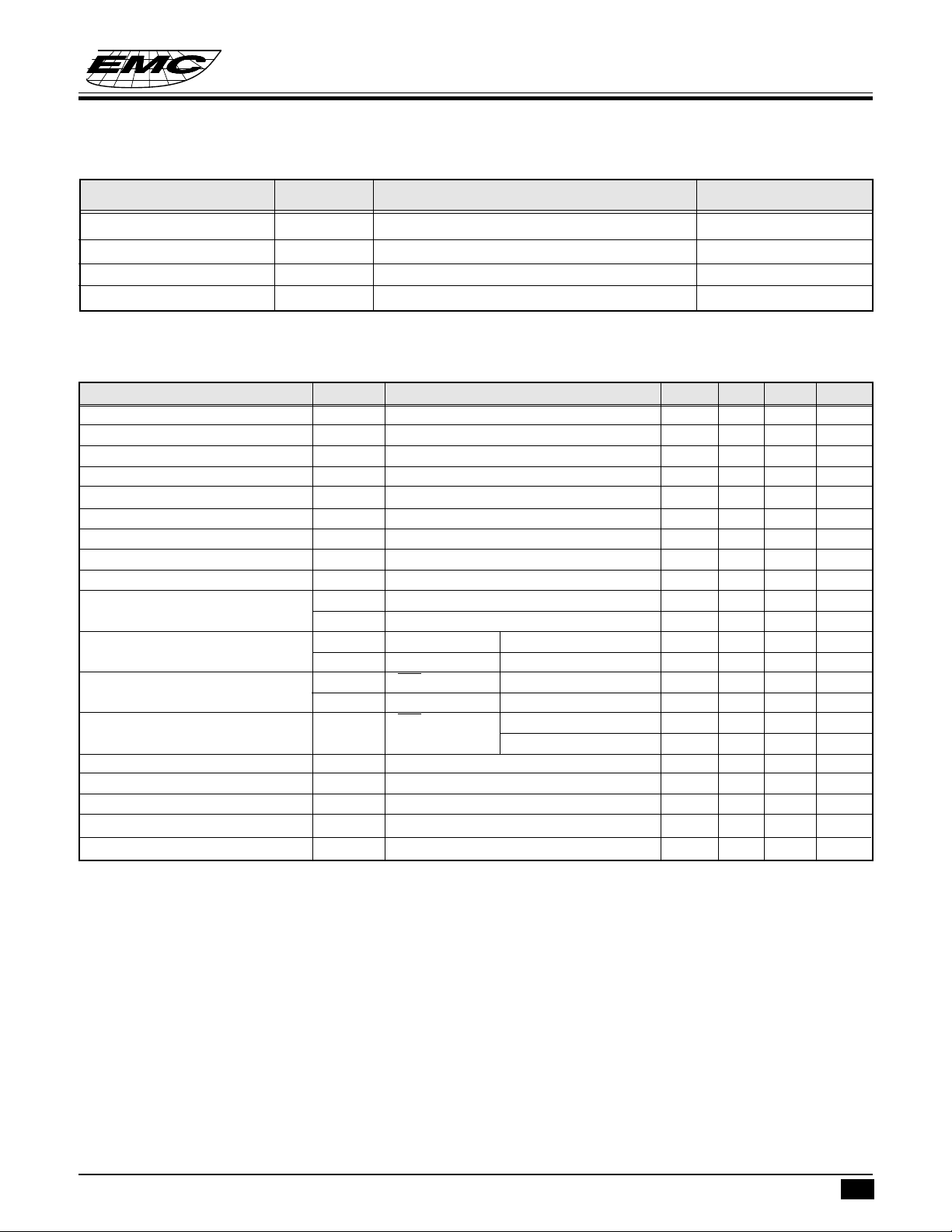
ABSOLUTE MAXIMUM RATINGS (T
=25°C)
A
Items Sym. Rating Unit
Supply voltage V
Analog input voltage V
Reference input voltage V
Operating temperature T
DD
IN
RT,VRB
OPR
7V
V
to V
SS
DD
V
to V
SS
DD
V
V
-20 to 65 °C
(FC=5MPS,AVDD=DVDD=5V,VRB=1.0V,VRT=4.0V,Ta=25°C)
Parameter Sym. Conditions Min. Typ. Max. Unit
Maximum Conversion Speed F
Supply current I
Reference pin current I
DD
REF
C
FC=5MSPS 23 28 mA
7.5 8.5 9.4 mA
5 8 MSPS
Analog input bandwidth BW 1 MHz
Analog input capacitance C
Reference resistance R
Differential reference voltage V
RT-VRB
Internal bias reference voltage V
V
RT-VRB
Digital input voltage V
Digital input current I
Digital output current I
Digital output current I
V
I
I
OZH
IN
REF
RB
IH
IL
IH
IL
OH
OL
320 355 400 Ω
External bias AVSS≤VRB ≤VRT ≤AV
Internal bias short VRB and V
Internal bias short VRT and V
RBS
RTS
1.0 V
DD
0.95 1.0 1.05 V
2.9 3.0 3.1
4.0 V
VDD=max. VIH=V
DD
VIL=0V 5
OE=VSS,V
OH=VDD
-0.5V -1.1 V
VDD=min. VOL=0.4V 3.7 V
OE=V
DD
VOH=V
V
DD
=0V 16 V
OL
5pF
1.0
5 µA
16 V
Output data delay TDL 20 30 ns
Integral nonlinearity EL ±2.0 LSB
Differential nonlinearity ED ±1.0 LSB
Aperture jitter t
Sampling delay t
aj
ds
50 ps
4ns
DD
* This specification are subject to be changed without notice.
5.26.1997
3
Page 4
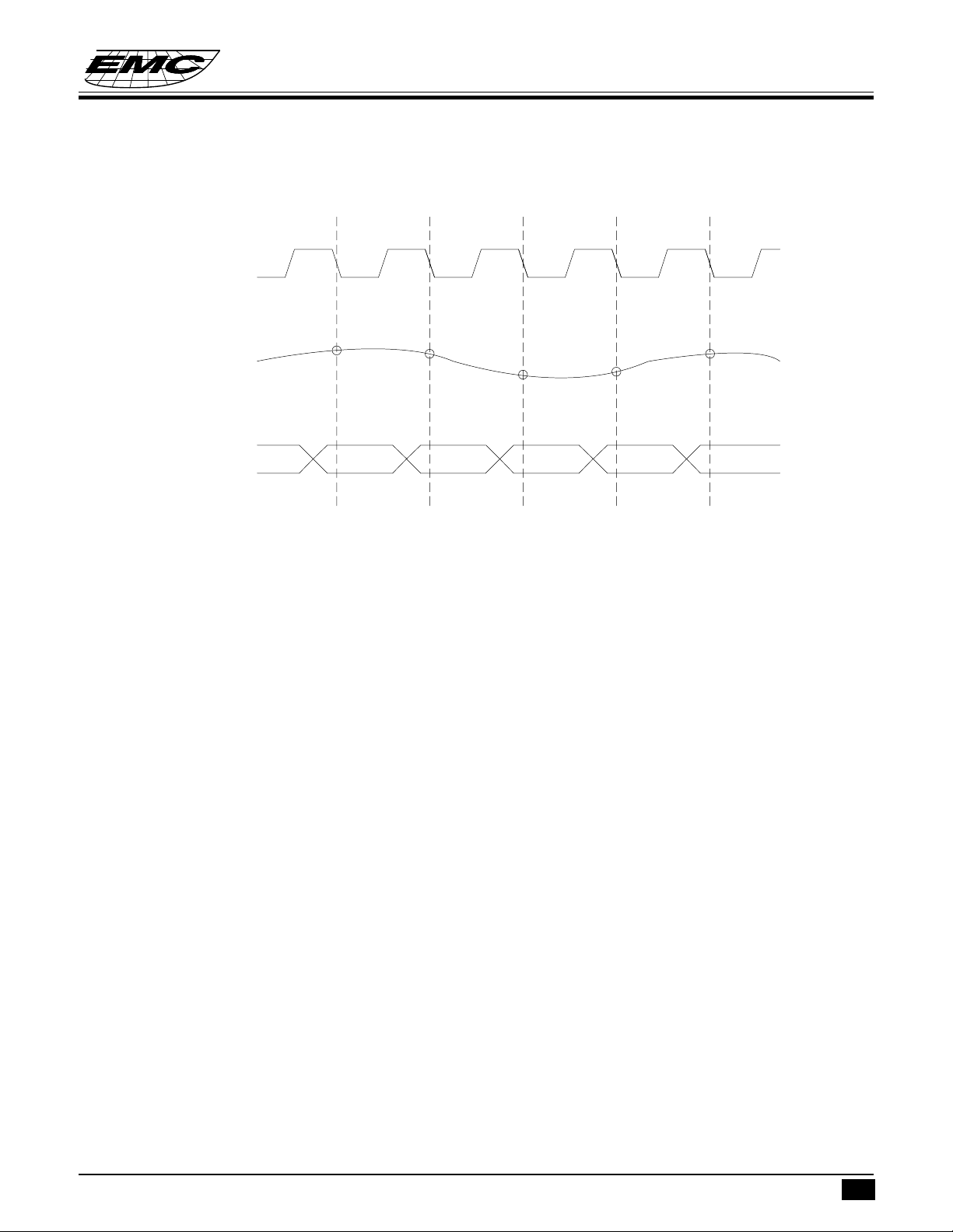
TIMING DIAGRAM
Clock
EM19110
10-BIT 5 MSPS A/D CONVERTER
Analog input
Data output
Application Note
1. AVDD ,DVDD ,VSS
To reduce noise effects, separate the analog and digital systems close to the device. For both the digital and
analog VDD pins, use a ceramic capacitor of about 0.1uF set as close as possible to the pin to bypass to the
respective GND’s.
2. Signal input Vi
Compared with the flash type A/D converter, the input capacitance of the analog input is rather small. However
it is necessary to conduct the drive with an amplifier featuring sufficient band and drive capability. When
driving with an amplifier of low output impedance, parasite oscillation may occur. That may be prevented by
inserting a resistance of about 100( in series between the amplifier output and A/D input.
N
N-3 N-2
N+1
N+2
N-1
N+3
N+4
N
N+1
3. Clock input
The clock line wiring should be as short as possible also, to avoid any interference with other signals, separate
it from other circuits.
4. Reference voltage
Voltage between VRT to VRB is compatible with the dynamic range of the analog input. Bypassing VRT and
VRB pins to GND, by means of a capacitor about 0.1uF, stable characteristics are obtained. By shorting VRT
and VRTS, VRB and VRBS, the self bias function that generates VRT=4.0V and VRB=1.0V, is activated.
Also, the users can setup external reference voltage by just connecting VRT and VRB to desired DC voltage
under spec.
5. Clock timing
* This specification are subject to be changed without notice.
5.26.1997
4
Page 5

EM19110
10-BIT 5 MSPS A/D CONVERTER
Analog input is sampled with the falling edge of CLK and output as digital data with a delay of 2.5 clocks and
with the following rising edge. The delay from the clock rising edge to the data output is the output data delay
about 20ns.
6. /OE
By connecting /OE to GND output mode is obtained. By connecting to VDD high impedance is obtained.
7. About latch up
It is necessary that AVDD and DVDD pins be the common source of power supply. This is to avoid latch up
due to the voltage difference between AVDD and DVDD pins when power is ON.
8. Tap reference voltage
Tap reference voltage VR1 thru VR3 connect to eighth point along the reference ladder; VR1 is 1/4th up from
VRB, VR2 is 2/4th up from VRB, VR3 is 3/4th up from VRB. These pins connecting 0.1uF capacitor to VSS
can stabilize the transfer characteristic. By connecting these pins to voltage sources, the piece wise linear
transfer curve can be attained.
* This specification are subject to be changed without notice.
5.26.1997
5
Page 6
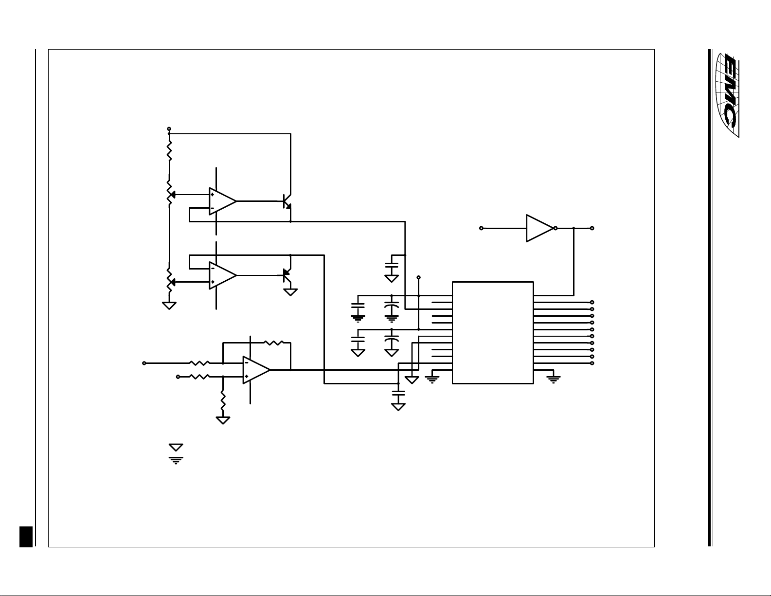
* This specification are subject to be changed without notice.
5V
R1
1k
APPLICATION CIRCUIT
5.26.1997
R2 1k
U1A
Q1
U2A
CLOCK IN
U1B
Q2
500
R3
C2
0.1u
R4
C4
0.1u
5V
R5
R6
Vi
U1C
R7
C6
0.1u
C1
10u
C3
10u
C5
0.1u
5V
U3
13
DVDD
14
VRTS
15
VRT
16
VR3
17
VR2
18
AVDD
19
VIN
20
AVSS
21
VR1
22
VRBS
23
VRB
24
DVSS
EM19110
CLK
D9
D8
D7
D6
D5
D4
D3
D2
D1
D0
/OE
12
11
10
9
8
7
6
5
4
3
2
1
CLK
D9(MSB)
D8
D7
D6
D5
D4
D3
D2
D1
D0(LSB)
10-BIT 5 MSPS A/D CONVERTER
--- Analog GND
--- Digital GND
EM19110
6
 Loading...