

Page 1

MOTION DETECTOR KIT
MODEL AK-510
Copyright © 2013, 1994 by ELENCO®Electronics, Inc. All rights reserved. Revised 2011 REV-P 753010
No part of this book shall be reproduced by any means; electronic, photocopying, or otherwise without written permission from the publisher.
ELENCO
®
Assembly and Instruction Manual
Page 2

PARTS LIST
If you are a student, and any parts are missing or damaged, please see instructor or bookstore.
If you purchased this kit from a distributor, catalog, etc., please contact ELENCO®(address/phone/e-mail is at
the back of this manual) for additional assistance, if needed. DO NOT contact your place of purchase as they
will not be able to help you.
RESISTORS
Qty. Symbol Description Color Code Part #
! 1 R16 300Ω 5% 1/4W orange-black-brown-gold 133000
! 1 R15 5.6kΩ 5% 1/4W green-blue-red-gold 145600
! 1 R5 39kΩ 5% 1/4W orange-white-orange-gold 153900
! 4 R1, 2, 8, 9 47kΩ 5% 1/4W yellow-violet-orange-gold 154700
! 1 R3 75kΩ 5% 1/4W violet-green-orange-gold 157500
! 1 R6 120kΩ 5% 1/4W brown-red-yellow-gold 161200
! 1 R14 270kΩ 5% 1/4W red-violet-yellow-gold 162700
! 2 R11, R12 300kΩ 5% 1/4W orange-black-yellow-gold 163000
! 1 R13 470kΩ 5% 1/4W yellow-violet-yellow-gold 164700
! 1 R10 510kΩ 5% 1/4W green-brown-yellow-gold 165100
! 1 R7 1.2MΩ 5% 1/4W brown-red-green-gold 171200
! 1 R4 1.6MΩ 5% 1/4W brown-blue-green-gold 171600
CAPACITORS
Qty. Symbol Value Description Part #
! 1 C8 470pF (471) Discap 224717
! 1 C9 .01µF (103) Discap 241031
! 2 C2, C3 10µF 25V Electrolytic (lytic) 271045
! 2 C4, C5 22µF 25V Electrolytic (lytic) 272245
! 2 C1, C6 100µF 16V Electrolytic (lytic) 281044
SEMICONDUCTORS
Qty. Symbol Value Description Part #
! 1 D1 1N4148 Diode 314148
! 1 Q1 MPSA18 Transistor NPN 320018
! 1 IC1 LM324 Integrated circuit 330324
! 1 IC2 HT2812G Integrated circuit 332812
! 1 IC3 78L05 Integrated circuit 338L05
! 1 S1 LHI-954 / KDS245 Infrared detector 350954
MISCELLANEOUS
Qty. Description Part #
! 1 PC board 517019
! 1 Speaker w/ wires 520813
! 1 Switch key 540105
! 1 SW1 - slide switch 541007
! 1 Battery snap 590098
! 1 Front cover 623104
! 1 Back cover 623202
! 1 Mounting bracket 626004
Qty. Description Part #
! 1 Battery cover 626005
! 2 Screw #4 x 1/4” 642430
! 2 Screw #4 x 5/8” 643450
! 2 Washer #4 (fiber) 645404
! 1 Socket IC 8-Pin 664008
! 1 Socket IC 14-Pin 664014
! 1 Solder lead-free 9LF99
Note:
The text printed on
the LHI-954 Infrared
Detector is the date code.
Resistor Battery Snap
Capacitor
PARTS
IDENTIFICATION
Electrolytic
Transistor
Integrated Circuit
Discap
Diode
Infrared Detector
Integrated
Circuit
Socket
Speaker
Switch
-1-
Page 3
-2-
Warning:
If the capacitor is
connected with
incorrect polarity, it
may heat up and
either leak, or
cause the capacitor
to explode.
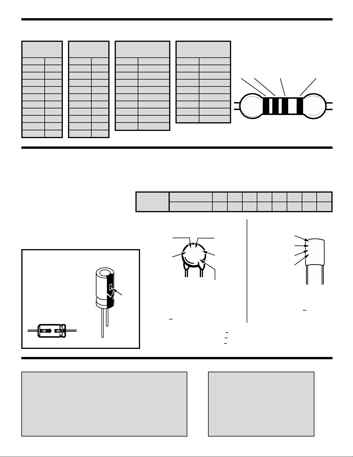
IDENTIFYING RESISTOR VALUES
Use the following information as a guide in properly identifying the value of resistors.
BANDS
METRIC UNITS AND CONVERSIONS
Abbreviation Means Multiply Unit By Or
p Pico .000000000001 10
-12
n nano .000000001 10
-9
µ micro .000001 10
-6
m milli .001 10
-3
– unit 1 10
0
k kilo 1,000 10
3
M mega 1,000,000 10
6
1. 1,000 pico units = 1 nano unit
2. 1,000 nano units = 1 micro unit
3. 1,000 micro units = 1 milli unit
4. 1,000 milli units = 1 unit
5. 1,000 units = 1 kilo unit
6. 1,000 kilo units = 1 mega unit
IDENTIFYING CAPACITOR VALUES
Capacitors will be identified by their capacitance value in pF (picofarads), nF (nanofarads), or µF (microfarads).
Most capacitors will have their actual value printed on them. Some capacitors may have their value printed in
the following manner. The maximum operating voltage may also be printed on the capacitor.
Electrolytic capacitors have a positive
and a negative electrode. The
negative lead is indicated on the
packaging by a stripe with minus
signs and possibly arrowheads. Also,
the negative lead of a radial
electrolytic is shorter than the positive
one.
Polarity
marking
BAND 1
1st Digit
Color Digit
Black 0
Brown
1
Red 2
Orange 3
Yellow 4
Green 5
Blue 6
Violet 7
Gray 8
White 9
BAND 2
2nd Digit
Color Digit
Black 0
Brown 1
Red 2
Orange 3
Yellow 4
Green 5
Blue 6
Violet 7
Gray 8
White 9
Multiplier
Color Multiplier
Black 1
Brown 10
Red 100
Orange 1,000
Yellow 10,000
Green 100,000
Blue 1,000,000
Silver 0.01
Gold 0.1
Resistance
Tole r ance
Color Toler ance
Silver ±10%
Gold ±5%
Brown ±1%
Red ±2%
Orange ±3%
Green ±0.5%
Blue ±0.25%
Violet ±0.1%
1
2 Multiplier Tolerance
Multiplier
For the No. 0 1 2 3 4 5 8 9
Multiply By 1 10 100 1k 10k 100k .01 0.1
(+)
(–)
(+)
(–)
Axial
Radial
Second digit
First digit
Multiplier
Tolerance*
Note: The letter “R” may be used at times
to signify a decimal point; as in 3R3 = 3.3
The letter M indicates a tolerance of +20%
The letter K indicates a tolerance of +10%
The letter J indicates a tolerance of +5%
Maximum working voltage
(may or may not appear
on the cap)
The value is 10 x 10 =
100pF, +10%, 50V
*
CERAMIC DISC MYLAR
First digit
Second digit
Multiplier
Tolerance*
2A222J
100V
The value is 22 x 100 =
2,200pF or .0022µF, +5%, 100V
101K
50V
Page 4
-3-
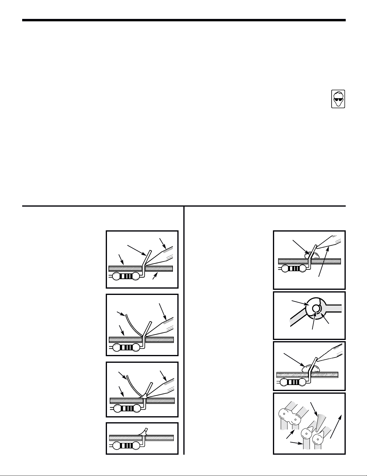
CONSTRUCTION
Solder
Soldering Iron
Foil
Solder
Soldering Iron
Foil
Component Lead
Soldering Iron
Circuit Board
Foil
Rosin
Soldering iron positioned
incorrectly.
Solder
Gap
Component Lead
Solder
Soldering Iron
Drag
Foil
1. Solder all components from the
copper foil side only. Push the
soldering iron tip against both the
lead and the circuit board foil.
2. Apply a small amount of solder to
the iron tip. This allows the heat
to leave the iron and onto the foil.
Immediately apply solder to the
opposite side of the connection,
away from the iron. Allow the
heated component and the circuit
foil to melt the solder.
1. Insufficient heat - the solder will
not flow onto the lead as shown.
3. Allow the solder to flow around
the connection. Then, remove
the solder and the iron and let the
connection cool. The solder
should have flowed smoothly and
not lump around the wire lead.
4.
Here is what a good solder
connection looks like.
2. Insufficient solder - let the
solder flow over the connection
until it is covered.
Use just enough solder to cover
the connection.
3. Excessive solder - could make
connections that you did not
intend to between adjacent foil
areas or terminals.
4. Solder bridges - occur when
solder runs between circuit paths
and creates a short circuit. This is
usually caused by using too
much solder.
To correct this, simply drag your
soldering iron across the solder
bridge as shown.
What Good Soldering Looks Like
A good solder connection should be bright, shiny, smooth, and uniformly
flowed over all surfaces.
Types of Poor Soldering Connections
Introduction
The most important factor in assembling your AK-510 Motion Detector
Kit is good soldering techniques. Using the proper soldering iron is of
prime importance. A small pencil type soldering iron of 25 watts is
recommended. The tip of the iron must be kept clean at all times
and well-tinned.
Solder
For many years leaded solder was the most common type of solder
used by the electronics industry, but it is now being replaced by leadfree solder for health reasons. This kit contains lead-free solder, which
contains 99.3% tin, 0.7% copper, and has a rosin-flux core.
Lead-free solder is different from lead solder: It has a higher melting
point than lead solder, so you need higher temperature for the solder to
flow properly. Recommended tip temperature is approximately 700OF;
higher temperatures improve solder flow but accelerate tip decay. An
increase in soldering time may be required to achieve good results.
Soldering iron tips wear out faster since lead-free solders are more
corrosive and the higher soldering temperatures accelerate corrosion,
so proper tip care is important. The solder joint finish will look slightly
duller with lead-free solders.
Use these procedures to increase the life of your soldering iron tip when
using lead-free solder:
● Keep the iron tinned at all times.
● Use the correct tip size for best heat transfer. The conical tip is the
most commonly used.
● Turn off iron when not in use or reduce temperature setting when
using a soldering station.
●
Tips should be cleaned frequently to remove oxidation before it becomes
impossible to remove. Use Dry Tip Cleaner (Elenco®#SH-1025) or Tip
Cleaner (Elenco®#TTC1). If you use a sponge to clean your tip, then use
distilled water (tap water has impurities that accelerate corrosion).
Safety Procedures
● Always wear safety glasses or safety goggles to
protect your eyes when working with tools or
soldering iron, and during all phases of testing.
● Be sure there is adequate ventilation when soldering.
●
Locate soldering iron in an area where you do not have to go around
it or reach over it. Keep it in a safe area away from the reach of
children.
● Do not hold solder in your mouth. Solder is a toxic substance.
Wash hands thoroughly after handling solder.
Assemble Components
In all of the following assembly steps, the components must be installed
on the top side of the PC board unless otherwise indicated. The top
legend shows where each component goes. The leads pass through the
corresponding holes in the board and are soldered on the foil side.
Use only rosin core solder.
DO NOT USE ACID CORE SOLDER!
Page 5
INTRODUCTION
The AK-510 is an infrared motion detector kit. The objective of the kit is to teach the operations of the four
sections that make up the kit. The four sections are shown in the block diagram below.
There are many applications for the use of the detector. The most common is in the alarm system industry.
Some of the new applications are automatic door openers, light switches in hallways, stairways and areas that
increase safety for the public. Further applications can be seen in automatic production lines, switching of
sanitary facilities, monitors and intercoms. With the ease of installation and the low suspectibility to interference
from other forms of radiation, such as heaters or windows, the IR detectors are ideal devices.
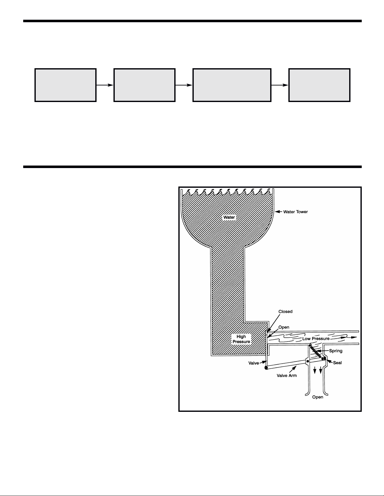
POWER SUPPLY (see page 16)
A 9 volt battery is used to supply the DC voltage to
the circuit. The battery voltage must be regulated
(held as close as possible) to 5 volts. This is done by
circuits called voltage regulators.
In order to see how this is accomplished, let’s
consider the analogy of a water tower. Voltage in
electronics can be compared to water pressure in
a water system. When water is pumped into a
water tower, the pressure at the bottom of the
tower can be quite high. In order to keep a
constant pressure in the water pipes that go to the
houses, the pressure must be lowered and held
constant.
Consider the system shown in Figure 1. As people
draw water into their homes, the pressure on the
low pressure side of the valve drops. The spring
pulls the valve arm inside the pipe up along
opening the valve and allowing more water into
the pipe. As the pressure on the low pressure side
increases, it pushes the valve arm inside the pipe
down closing the valve and stretching the spring.
By increasing the spring pressure on the arm, the
pressure on the low side will have to increase to
close the valve. The force or pressure of the
spring, therefore sets the value of the pressure on
the low pressure side of the system. The force of
the spring is called the reference pressure.
Voltage in electronics is the analogy to pressure in water pipes. A voltage greater than 7V is applied to the
input of high voltage side of the regulator. A fixed reference voltage inside the regulator will set the low voltage
output at 5 volts +5%. This is accomplished in a manner very similar to our water tower analogy. The output
voltage is filtered or made smooth (no ripples) by capacitor C6 (100µF).
POWER
SUPPLY
TONE
GENERATOR
INFRARED
DETECTOR
OPERATIONAL
AMPLIFIERS
FILTERS
-4-
Figure 1
Page 6
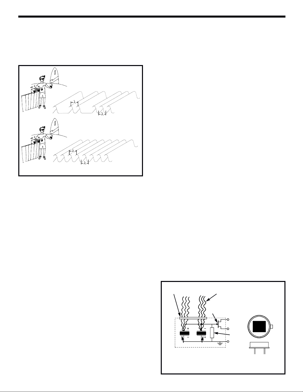
INFRARED DETECTOR
Infrared light was first discovered back in 1801 by W.
Herschel. Infrared is a form of radiated energy in
which the wavelength is longer than the wavelength
of visible light. A wavelength can best be understood
by the physical analogy shown in Figure 2.
If you were standing at the beach watching the
waves come in to shore, you would be able to see
the peaks of each wave as they approached. If you
could measure the distance from one peak to the
next, you would know the “Wavelength” of those
waves. We will use the eleventh letter of the Greek
alphabet “λ” (lambda) to represent the distance
between valleys to determine the length of the wave
(see Figure 2). A wavelength can be defined as the
distance between any two exactly equal points on
identically repeating waves.
What would happen if we reduced the distance
between the peaks to 1/2 the original distance.
Would it not be true, the peaks would strike the
shore twice as often as before? The frequency of
the peaks reaching the shore would be twice that of
the longer wave. For people who like big words, we
would say “Frequency is inversely proportional to
the wavelength”. In simple words, “If the wavelength
goes up, the frequency goes down and if the
wavelength goes down, the frequency goes up”.
The mathematics of waves applies also to the
radiation of light. It is common practice, therefore,
to talk about light as lightwaves. The wavelength of
infrared light ranges from 0.78 micrometers (µm) to
100 (µm). A micrometer is one millionth of a meter.
Infrared can be thought of as heat radiation
because the radiant energy is transformed into heat
when it strikes a solid surface. All solid bodies at a
temperature above absolute zero emit thermal
radiation. As a body’s temperature rises, the shorter
the resulting wavelengths become. The human
body’s maximum thermal radiation is between 9µm
and 10µm in the infrared stage. Motion can be
detected by special elements which are highly
sensitive in the infrared range. Such devices are
called Pyroelectric Infrared Detectors.
PYROELECTRIC EFFECT
When certain materials change temperature, they
produce electricity. A Pyroelectric crystal is an
example of such a material. If a Pyroelectric crystal
has been at the same temperature for a period of
time, there will be no voltage across it’s electrodes.
When the crystal temperature changes, a voltage is
produced at the electrodes of the crystal element.
This type of crystal is used in this motion detector kit
inside the infrared (IR) detector.
INTERNAL DESIGN
The IR detector contains two crystals connected
with each other in opposite polarity and with a 1
millimeter (mm) optical spacing. These two crystals
are located behind an optical filter or lens (see
Figure 3). The output power of the crystals is very
low. A special device called the Field Effect
Transistor (FET) is used to increase the power
output. The FET can be compared to water pipes as
shown in Figure 4. The center of a small section of
pipe is made of thin, flexible rubber surrounded by
water from a third pipe called the gate. When
pressure (voltage) is applied to the gate, the rubber
tube closes and pinches off the flow of water
(current) from source to drain. In a similar manner,
as infrared radiation is detected, the crystals
produce a voltage at the gate
of the FET.
-5-
Figure 3
Figure 2
Infrared RaysOptical Filter
Gate
Drain
Source
Resistor
Ground
Crystals
Dual Element Detector Scheme
Page 7

This causes a change in current from the drain to
source. Very little power is required at the gate to
control the larger current flow from source to drain.
The benefits of this type of detector are low radio
interference, low noise, specially suited response.
The IR detector is sealed in a metal housing to
prevent electromagnetic interference and to keep
them clean.
FIELD OF VIEW
Detectors are available with different fields of view,
depending on the application. The maximum
distance and total angle of view are important
specifications needed in choosing a motion detector.
The LHI-954 field of view is shown in Figure 5.
CIRCUIT DESCRIPTION (see page 16)
The IR Section contains only a few components,
R1, R2, C1 and the PIR sensor. As motion is
detected, the IR detector will produce a voltage at
the gate of the FET allowing current to flow from the
drain to source, causing the voltage at the input of
U1 (pin 13) to change, thus changing the output at
pin 14. Resistors R1 and R2 limit the amount of
current flow through the FET.
-6-
An amplifier is a device that uses a small amount
of power to control a larger amount of power. Just
like a small amount of power on the valve arm of
Figure 1 controlled the water pressure in the pipes
going to the houses. The amplifier does not create
power (it was already there in the water tower) but
it controls the power from a source.
In electronics, amplifiers are composed of devices
called transistors, resistors, and capacitors. The
number of these components used and the way
they are assembled determines the characteristics
of the amplifier. An amplifier that can perform many
mathematical operations such as adding,
subtracting, or multiplying voltages is called an
Operational Amplifier or Op-Amp.
The characteristics of an ideal op-amp are the
following:
A. infinite voltage gain (no voltage at all on the
input controls, large voltage on the output).
B. infinite bandwidth (no matter how fast the input
changes, the output will change just as fast).
C. infinite input impedance (no power required at
input to change output).
D. zero output impedance (the output can deliver
an infinite amount of power).
Obviously, in the real world these conditions can
never be met, but for mathematical purposes they
are assumed in designing electronic circuits with
op-amps.
The op-amp has two input terminals, inverting input
(–) and non-inverting input (+), and one output
terminal. Figure 6 shows the standard op-amp
symbol. The two input terminals are labeled 2 and 3,
and the output is 1. Most op-amps operate with two
DC power supplies, +VCC and –VEE connect to pins
11 and 4 respectively. Since a single power supply
is used in the kit, –VEE (pin 4) is tied to ground. The
op-amp multiplies the difference between the
voltage signals applied at its two input terminals
(V3-V2) times the gain of the amplifier (A). A x (V3V2) appears at the output terminal as shown in
Figure 7.
OPERATIONAL AMPLIFIERS / FILTERS
Figure 4
Gate
Drain
Source
FET Transistor
Horizontal
Figure 5
Vertical
56
O
56
O
46
O
46
O
Figure 6 Figure 7
Inverting
Input
Non-
Inverting
Input
2
3
4
11
1
Output
+Vcc
–VEE
2
3
4
11
1
Output
A (V3 - V2)
+Vcc
–VEE
V2
V3
Page 8

-7-
Figure 9
NEGATIVE FEEDBACK
The open loop gain (or maximum gain) of a typical
op-amp is very high (usually greater than 100,000),
enabling a very small input voltage to drive the opamp output to its extremes. To prevent this, a resistor
is connected between the output and inverting input
terminals allowing a portion of the output signal to be
brought back and cancel part of the input (Figure 8).
This process is called Negative Feedback. The signal
being fed back is out of phase with the input and thus
subtracts from the input signal. If the resistor was
connected between the non-inverting input and
output terminals, it would be called Positive
Feedback. The closed loop gain (or gain after
feedback) from the input Vito the output terminal
depends on the ratio of R2 to R1.
For example, if R2 = 100 and R1 = 10, the gain (G)
= R2/R1 = 100/10 = 10. Thus, the output voltage V
o
would be equal to –10(Vi). The (–) sign indicates that
the output and input voltages are of opposite polarity.
VOLTAGE COMPARATOR
Operational amplifiers can be used to compare the
amplitude of one voltage with another. As a
comparator, its function is to determine when an
input voltage exceeds a certain level. When used as
a comparator, the op-amp is used without feedback
and at maximum gain. One input is set to a
reference voltage and the other tied to the input
voltage.
Figure 8
LOW PASS FILTER
A low pass filter attenuates (decreases) all signals
above a certain frequency and passes frequencies
below that frequency. An example of a low pass filter
is a simple RC network as shown in Figure 9. Low
frequencies are passed unharmed. As the frequency
rises the output is reduced (see Figure 10).
HIGH PASS FILTER
The high pass filter attenuates frequencies below a
certain frequency and passes frequencies above that
frequency. An example of a high pass filter is a simple
RC network as shown in Figure 11. Low frequencies
are reduced when passed through the filter while high
are passed unharmed (see Figure 12).
FILTERS
Figure 10
Figure 11
Figure 12
R1
R2
V
i
2
3
1
V
o
Vo= –(R2/R1) V
i
OR
Vo= –G V
i
Page 9

-8-
Figure 15
Key
Output
BAND PASS FILTER
The combination of a low and high pass filter create
what is called a Band Pass Filter. The frequencies
passed by each filter overlap and create a bandwidth
(range), passing all signals within the bandwidth and
reducing all others. Figure 13 illustrates the general
band-pass response curve. A critical frequency is
defined as the point where the voltage is reduced to
0.707 (the square root of ½ is used because it
represents the point where power has been reduced
to ½). The bandwidth can be defined as the difference
between the upper critical frequency (fC2) and the
lower critical frequency fC1 (BW = fC2 - fC1). The
selectivity (or Quality) of a band-pass filter is
expressed as the “Q” of the filter.
It is the ratio of the center (or Resonant) frequency to
the bandwidth (Q = fr/BW). A filter with a higher value
of Q has a narrower bandwidth, thus passing fewer
frequencies than one with a lower value. Bandpass
filters can be classified as either a narrow-band (Q >
10) or a wide-band (Q < 10).
CIRCUIT DESCRIPTION (See page 16)
The op-amp IC1D shapes the frequency response
to amplify those frequencies produced when motion
is detected and rejects all others, such as those due
to noise or slow temperature changes. Frequencies
above 20Hz and below 1Hz are beyond the
bandwidth of the circuit and thus are rejected. The
output at pin 14 is about 1.6V when no motion is
detected. As motion is detected, the voltage at the
output will change and trigger either IC1C or IC1B.
The op-amps IC1A, IC1B and IC1C are configured
as voltage comparators. In the ready state, the
output of IC1A is high and IC1B and IC1C are low.
When IC1D outputs a voltage lower than 1.41V, it
will force pin 2 of IC1 high. When IC1D outputs a
voltage higher than 1.67V, it forces pin 8 and pin 2 of
IC1 to go high. A high in with one of these cases
causes the output to go low and allows C9 to
discharge through IC1A. The discharging of C9 will
pull pin 6 of IC2 low and trigger the sound generator.
Figure 13
The circuit uses the single sound generator HT2812G
IC. The HT2812G is a CMOS LSI chip designed for
use in sound effects products. Figure 14 shows the
internal design of the IC.
CIRCUIT DESCRIPTION (see page 16)
As the Key Input is brought low, the Oscillator, Speed
Generator, Tone Generator, Noise Generator and
Envelope Sections are all enabled. The Oscillator
Section begins to oscillate at a frequency determined
by the voltage across pins 7 and 8. This frequency is
then divided down and applied to the Speed
Generator. The Speed Generator controls the
frequency of the output as it is applied to the output
driver. The output consists of 15 pulses. Appling the
pulses to the base of transistor Q1, turns it on and off
rapidly, causing the speaker to sound. You can select
between a high and a low tone using switch SW1.
SOUND GENERATOR
Figure 14
Osc1
Osc2
Oscillator
Key
Key
Input
Logic
Selector
and
Envelope
Circuit
Divider
Speed
Generator
To ne
Generator
Noise
Generator
Output
Driver
Env
Output
Output
Gain
BW
100%
70.7%
fc1 fr fc2
f
Page 10

-9-
ASSEMBLE COMPONENTS TO THE PC BOARD
Note: C7 is not used in this kit.
Figure D
These capacitors are
polarized. Be sure to
mount them with the “+”
lead in the correct hole as
marked on the PC board.
Warning: If the capacitor
is connected with incorrect
polarity it may heat up and
either leak or cause the
capacitor to explode.
Figure B
Mount the device with the flat
side in the same direction as
shown on the PC board. Solder
and cut off the excess leads.
Figure C
Align the socket notch (if any)
with the notch marked on the
PC board.
Solder the socket to the PC
board. Insert the IC into the
socket with the notch as shown
below.
R2 - 47kΩ 5% 1/4W Resistor
(yellow-violet-orange-gold)
C2 - 10µF 25V Electrolytic
(see Figure D)
C4 - 22µF 25V Electrolytic
(see Figure D)
R5 - 39kΩ 5% 1/4W Resistor
(orange-white-orange-gold)
R3 - 75kΩ 5% 1/4W Resistor
(violet-green-orange-gold)
C8 - 470pF (471) Discap
D1 - 1N4148 Diode
(see Figure A)
R4 - 1.6MΩ 5% 1/4W Resistor
(brown-blue-green-gold)
(See Note)
R6 - 120kΩ 5% 1/4W Resistor
(brown-red-yellow-gold)
(See Note)
R9 - 47kΩ 5% 1/4W Resistor
(yellow-violet-orange-gold)
14-pin IC Socket
IC1 - LM324 Integrated Circuit
(see Figure C)
R12 - 300kΩ 5% 1/4W Resistor
(orange-black-yellow-gold)
R11 - 300kΩ 5% 1/4W Resistor
(orange-black-yellow-gold)
R10 - 510kΩ
5% 1/4W
Resistor
(green-brown-yellow-gold)
C9 - .01µF (103) Discap
C6 - 100µF 16V Electrolytic
(see Figure D)
IC3 - 78L05 Integrated Circuit
(see Figure B)
D2 - Use a Jumper Wire in
place of the diode.
C5 - 22µF 25V Electrolytic
(see Figure D)
Figure A
Diodes have polarity. Be sure to mount them with the band
going in the same direction as marked on the PC board.
Band
Polarity
marking
(–) (+)
Flat
Notch
Page 11

-10-
ASSEMBLE COMPONENTS (CONTINUED)
+
Inside Pads
Outside Pads
Note: The text printed
on the LHI-954
Infrared Detector is
the date code.
Figure E
Use a discarded lead for
a jumper wire.
Jumper Wire (see Figure E)
C1 - 100µF 16V Electrolytic
(see Figure D)
R1 - 47kΩ
5% 1/4W
Resistor
(yellow-violet-orange-gold)
C3 - 10µF 25V Electrolytic
(see Figure D)
R8 - 47kΩ
5% 1/4W
Resistor
(yellow-violet-orange-gold)
R7 - 1.2MΩ
5% 1/4W
Resistor
(brown-red-green-gold)
S1 - LHI-954
Infrared Detector
Mount with tab in the same direction as
marked on the PC board (see note below).
R14 - 270kΩ
5% 1/4W
Res.
(red-violet-yellow-gold)
R13 - 470kΩ
5% 1/4W
Resistor
(yellow-violet-yellow-gold)
SW1 - Slide Switch
R16 - 300Ω
5% 1/4W
Resistor
(orange-black-brown-gold)
8-pin IC Socket
IC2 - HT2812G
Integrated Circuit
(see Figure C)
Q1 - MPSA18 Transistor
(see Figure B)
R15 - 5.6kΩ 5% 1/4W Resistor
(green-blue-red-gold)
Speaker Wires - Solder the
two wires to the PC board
marked SPK +, –.
Note: If wires need resoldering;
1. First apply a small amount of
solder to the outside pad.
2. Solder the speaker wire to
the outside pads.
CAUTION: The internal
speaker wires are soldered to
the inside pads. DO NOT
unsolder these wires.
B1 - Battery Snap
Identify the battery snap B1. Insert the red and black wires
through the hole from the copper side of the PC board.
Insert the red wire into the (+) positive hole and the black
wire into the (–) negative hole as shown above.
Red
Black
–
Page 12

FINAL ASSEMBLY
-11-
! Step 1
Place the speaker into the front case as
shown in Figure 16. Use two #4 x 1/4”
screws and two #4 washers to secure it
into place.
! Step 2
Push the switch key onto the switch as
shown in Figure 17. Make sure that the
key-switch is sitting properly on the
switch.
! Step 3
Place the PC board into the front case
as shown in Figure 18. Attach the back
case to the front case with two #4 x 5/8”
screws. Note: There is a small groove
that the key switch fits into.
Figure 16
#4 x 1/4” Screws
#4 Washers
Figure 17
Switch Key
Figure 18
Page 13

-12-
! Step 4
Attach a 9V battery to the battery snap
and place it into the case. Snap the
battery cover into the back case as
shown in Figure 19.
Figure 19
Battery Cover
! Step 5
Place the unit onto a table and turn it on.
Move to one side of the detector so that
you are out of the field of view of the
detector. Walk in front of the detector and
a tone will sound from the speaker. The
unit is now ready for use.
Note: When the switch is in the OFF position, it disconnects the voltage to the
sound generator IC only. The rest of the circuit is still operating. The battery will
run down if it is left in the OFF position. To increase battery life, remove the
battery if you intend to leave the unit in the OFF position for long periods of time.
INSTALLATION
The detector can be either placed on a
flat surface or mounted onto a wall.
Adjust the angle lever to the open
position (see Figure 20). Align the two
taps on the bracket with the two grooves
on the case. Adjust for the desired angle
and move the angle lever to the lock
position.
Figure 20
Angle Lever
Open
Plastic Bracket
Angle Lever
Closed
Page 14

-13-
TROUBLESHOOTING GUIDE
The values given below are approximate.
POWER SUPPLY
1. Measure the voltage at IC3. Pin 3 = 9V, Pin 1 = 4.75 - 5.25V
A. Check soldering around IC3 and C6.
B. Check for short to GND from pins 2 and 3.
C. If no shorts are present, IC3 may be defective.
INFRARED DETECTOR
2. Measure the voltages at points: A = 5V
B = 4.25V
C = .700V
A. Voltage at point A incorrect:
1. Check R1.
2. Check for a short between point A and GND.
B. Voltage at point B incorrect:
1. Check R1, C1 for correct value.
2. Check for a short between point B and GND.
C. Voltage at point C incorrect:
1. Check R2, C2 for correct value.
2. Check for a short between point B and GND.
C
B A
OPERATIONAL AMPLIFIERS
3. Measure the voltages at IC1 while the unit is at standby.
Pin Voltage Pin Voltage
1 3.80V 8 –
2 – 9 1.62V
3 1.40V 10 1.60V
4 5.00V 11 –
5 1.40V 12 1.52V
6 1.60V 13 1.55V
7 – 14 1.50 - 1.60V
Page 15

-14-
4. Measure the voltages at IC1 when activated.
A. Incorrect voltage readings:
1. Check resistors R3 - R12 for correct value.
2. Check diode D1 polarity.
3. Check C3 and C4 polarity.
4. IC1 may be defective.
SOUND GENERATOR
Measure the voltage at the following pins on U2, as listed in the chart below.
A. No voltage at pin 3:
1. Check R13, R14, SW1 and C5.
B. No 5V at pin 5:
1. Check SW1 solder connection.
2. No 5V at pin 6.
3. Check C9.
C. Outputs two short tones:
1. Check C5.
Pin Voltage
1 0 - 3.8V
7 0 - 3.8V
8 0 - 3.8V
14 1.5 - 3.8V
U2 Voltage Voltage
Pin No Sound Sound
3 0 0 - 4V
5 5V 5V
6 5V
7 0V .735V
Q1 Voltage Voltage
Pin No Sound Sound
E 0 0V
B 0V .355V
C 9V 7 - 9V
Q1
E B C
Page 16

-15-
QUIZ
1. The 9V battery supplies a . . .
! A. positive AC voltage.
! B. DC voltage.
! C. AC voltage.
! D. rectified DC voltage.
2. A human’s maximum thermal radiation is between . . .
! A. 3 and 5µm.
! B. 9 and 13µm.
! C. 10 and 20µm.
! D. 9 and 10µm.
3. As temperature changes, the pyroelectric crystals generate . . .
! A. white light.
! B. infrared light.
! C. heat.
! D. a voltage.
4. A wavelength is the distance between two points having . . .
! A. opposite phases.
! B. two different phases.
! C. the same phase, but different voltages.
! D. the same phase and voltage.
5. Infrared can be thought of as heat radiation because the . . .
! A. electrical energy is transformed into heat.
! B. radiant energy is transformed into heat.
! C. mechanical energy is transformed into heat.
! D. solar energy is transformed into heat.
6. What are the two inputs called in an op-amp?
! A. non-inverting and inverting.
! B. V1 and V2.
! C. VEE and VCC.
! D. gates.
7. A high pass filter attenuates all signals . . .
! A. between two frequencies.
! B. below the critical frequency.
! C. above the critical frequency.
! D. with high amplitudes.
8. The formula for the closed loop gain is . . .
! A. (R2 x R1)Vo
! B. (R1/R2)Vi
! C. (R2/R1)Vo
! D. -(R2/R1)Vi
9. A low pass filter attenuates all signals . . .
! A. between two frequencies.
! B. below the critical frequency.
! C. above the critical frequency.
! D. with low amplitudes.
10. A filter with a high value in Q has a . . .
! A. wide bandwidth.
! B. narrow bandwidth.
! C. long bandwidth.
! D. attenuates less frequencies.
Answers: 1. B, 2. D, 3. D, 4. D, 5. B, 6. A, 7. B, 8. D, 9. C, 10. B
Page 17

-16-
SCHEMATIC DIAGRAM
Page 18

-17-
SPECIFICATIONS
Power
• 9V DC battery
Current
• Operating 60mA (average)
• Standby Typical less than 4mA
Detection
• Pyroelectric Infrared Sensor.
Detection Distance
• 10 feet max., best at 1’ to 6’
Output Sound
• High frequency / Low frequency tone (15-pulse siren)
• 85 - 90dB peak
Operating Range
• –10 to +50OC
GLOSSARY OF TERMS
Amplify To enlarge or increase.
Amplitude The greatest difference above a reference, usually zero.
Analogy Likeness or resemblance in relations of different objects.
Attenuate To weaken or reduce.
Bandwidth The group or number of frequencies unaffected by a filter.
Battery A device that generates an electric current through a chemical reaction.
Capacitors Devices that store electronic charges.
Circuit The entire line through which electric current may pass.
Closed Loop Gain Gain after feedback.
Comparator An electronic device to detect voltage differences.
Critical Frequency The frequency at which power in a filter falls to half.
Crystals An inorganic body with plane surfaces in a geometrical form.
Current The flow of electrons.
Detector A device that changes signals into useful information.
Electromagnetic A radiated wave having both electric and magnetic properties.
FET Field Effect Transistor.
Filter A device used to nullify certain waves without altering others.
Frequency The repeated occurance of anything at brief intervals.
Gain To increase or make larger.
Gate A device used to allow or restrict passage.
Generator A device that transforms energy into electric power or signals.
Impedance A device’s resistance to the passage of electrical current.
Infrared Light Rays past the red end of the visible light spectrum.
IR Detector A device that senses the presence of infrared light.
Kit A collection of equipment or components.
Lambda The eleventh letter of the Greek Alphabet.
Page 19

-18-
Low Pass Filter Decreases all signals above a certain frequency and passes frequencies below
that frequency.
Negative Feedback To allow a portion of the output signal to be brought back and cancel part of the
input.
Noise A random, persistent disturbance of a signal.
Open Loop Gain The maximum gain available without feedback.
Oscillator A device used to vary between alternate extremes (varies from high to low).
Peak The top of a wave or mountain.
Polarity The division of two opposites.
Power Electrical energy; strength, force, or might.
Pyroelectric Effect When certain metals change temperature, they produce energy.
RC Network An assembly of resistors and capacitors.
Reference Voltage Level of electronic element used for providing resistance in a circuit.
Resistor An electric element used for providing resistance in a circuit.
Response Curve The shape of an output produced by a circuit.
Solder An alloy (mixture) of tin and lead used in the melted state to join or repair metal
parts.
Transistor A three-terminal semiconductor device used for amplification, switching, and
detection.
Valve
A mechanical device that regulates the flow of gases, liquids, or loose materials by
blocking and uncovering openings.
Voltage An electromotive force.
Wavelength The distance in a periodic wave between 2 points of corresponding phases.\
For further information on infrared light and waves . . .
The Invisible World of the Infrared
By Jack R. White
New York: Dodd, Mead, © 1984
124 p.; ill.
Waves and Vibrations
By Brian Knapp
Danbury, CT: Grolier, © 1994
48 p.; ill.
Page 20

ELENCO
®
150 Carpenter Avenue
Wheeling, IL 60090
(847) 541-3800
Web site: www.elenco.com
e-mail: elenco@elenco.com
 Loading...