

Page 1

BASIC ELECTRONIC COMPONENTS
MODEL ECK-10
Instruction Manual
by Arthur F. Seymour MSEE
It is the intention of this course to teach the fundamental operation of basic
electronic components by comparison to drawings of equivalent mechanical
parts. It must be understood that the mechanical circuits would operate much
slower than their electronic counterparts and one-to-one correlation can never
be achieved. The comparisons will, however, give an insight to each of the
fundamental electronic components used in every electronic product.
Resistors
Capacitors Coils
Semiconductors
Others
Transformers
ELENCO
®
Copyright © 2012, 1994 by Elenco®Electronics, Inc. All rights reserved. Revised 2012 REV-M 753254
No part of this book shall be reproduced by any means; electronic, photocopying, or otherwise without written permission from the publisher.
Page 2

-1-
RESISTORS
RESISTORS,
What do they do?
The electronic component known as the resistor is
best described as electrical friction. Pretend, for a
moment, that electricity travels through hollow pipes
like water. Assume two pipes are filled with water
and one pipe has very rough walls. It would be easy
to say that it is more difficult to push the water
through the rough-walled pipe than through a pipe
with smooth walls. The pipe with rough walls could
be described as having more resistance to
movement than the smooth one.
Pioneers in the field of electronics thought electricity
was some type of invisible fluid that could flow
through certain materials easily, but had difficulty
flowing through other materials. In a way they were
correct since the movement of electrons through a
material cannot be seen by the human eye, even
with the best microscopes made. There is a
similarity between the movement of electrons in
wires and the movement of water in the pipes. For
example, if the pressure on one end of a water pipe
is increased, the amount of water that will pass
through the pipe will also increase. The pressure on
the other end of the pipe will be indirectly related to
the resistance the pipe has to the flow of water. In
other words, the pressure at the other end of the
pipe will decrease if the resistance of the pipe
increases. Figure 1 shows this relationship
graphically.
Electrons flow through materials when a pressure
(called voltage in electronics) is placed on one end
of the material forcing the electrons to “react” with
each other until the ones on the other end of the
material move out. Some materials hold on to their
electrons more than others making it more difficult
for the electrons to move. These materials have a
higher resistance to the flow of electricity (called
current in electronics) than the ones that allow
electrons to move easily. Therefore, early
experimenters called the materials
insulators
if they
had very high resistance to electon flow and
conductors
if they had very little resistance to
electron flow. Later materials that offered a medium
amount of resistance were classified as
semiconductors
.
When a person designs a circuit in electronics, it is
often necessary to limit the amount of electrons or
current that will move through that circuit each
second. This is similar to the way a faucet limits the
amount of water that will enter a glass each second.
It would be very difficult to fill a glass without
breaking it if the faucet had only two states, wide
open or off. By using the proper value of resistance
in an electronic circuit designers can limit the
pressure placed on a device and thus prevent it from
being damaged or destroyed.
SUMMARY: The resistor is an electronic
component that has electrical friction. This friction
opposes the flow of electrons and thus reduces the
voltage (pressure) placed on other electronic
components by restricting the amount of current that
can pass through it.
Figure 1
Low Resistance
Pipe
High Resistance
Pipe (rough walls)
Low Pressure
High Pressure
Through Same
Size Opening
Water Tank
Page 3

-2-
RESISTORS
RESISTORS,
How are they made?
There are many different types of resistors used in
electronics. Each type is made from different
materials. Resistors are also made to handle
different amounts of electrical power. Some
resistors may change their value when voltages are
placed across them. These are called voltage
dependent resistors or
nonlinear
resistors. Most
resistors are designed to change their value when
the temperature of the resistor changes. Some
resistors are also made with a control attached that
allows the user to mechanically change the
resistance. These are called variable resistors or
potentiometers. Figure 2 shows physical shapes of
some different types of resistors.
The first commercial resistors made were formed by
wrapping a resistive wire around a non-conducting
rod (see Figure 3). The rod was usually made of
some form of ceramic that had the desired heat
properties since the wires could become quite hot
during use. End caps with leads attached were then
placed over the ends of the rod making contact to
the resistive wire, usually a nickel chromium alloy.
The value of wirewound resistors remain fairly flat
with increasing temperature, but change greatly with
frequency. It is also difficult to precisely control the
value of the resistor during construction so they
must be measured and sorted after they are built.
By grinding carbon into a fine powder and mixing it
with resin, a material can be made with different
resistive values. Conductive leads are placed on
each end of a cylinder of this material and the unit is
then heated or cured in an oven. The body of the
resistor is then painted with an insulating paint to
prevent it from shorting if touched by another
component. The finished resistors are then
measured and sorted by value (Figure 4). If these
resistors are overloaded by a circuit, their resistance
will permanently decrease. It is important that the
power rating of the carbon composition resistor is
not exceeded.
Figure 2
Carbon Film
Variable
Carbon Composition
THE WIREWOUND RESISTOR
Figure 3
THE CARBON COMPOSITION RESISTOR
Ceramic Rod
Wire
End CapProtective Coating
Figure 4
Insulating Paint Carbon & Resin
Mixture
Conductive Wire
Page 4
-3-
RESISTORS
CARBON FILM RESISTORS
Carbon film resistors are made by depositing a very
thin layer of carbon on a ceramic rod. The resistor
is then protected by a flameproof jacket since this
type of resistor will burn if overloaded sufficiently.
Carbon film resistors produce less electrical noise
than carbon composition and their values are
constant at high frequencies. You can substitute a
carbon film resistor for most carbon composition
resistors if the power ratings are carefully observed.
The construction of carbon film resistors require
temperatures in excess of 1,000
O
C.
Metal oxide resistors are also constructed in a
similar manner as the carbon film resistor with the
exception that the film is made of tin chloride at
temperatures as high as 5,000
O
C. Metal oxide
resistors are covered with epoxy or some similar
plastic coating. These resistors are more costly than
other types and therefore are only used when circuit
constraints make them necessary.
Metal film resistors are also made by depositing a
film of metal (usually nickel alloy) onto a ceramic
rod. These resistors are very stable with
temperature and frequency, but cost more than the
carbon film or carbon composition types. In some
instances, these resistors are cased in a ceramic
tube instead of the usual plastic or epoxy coating.
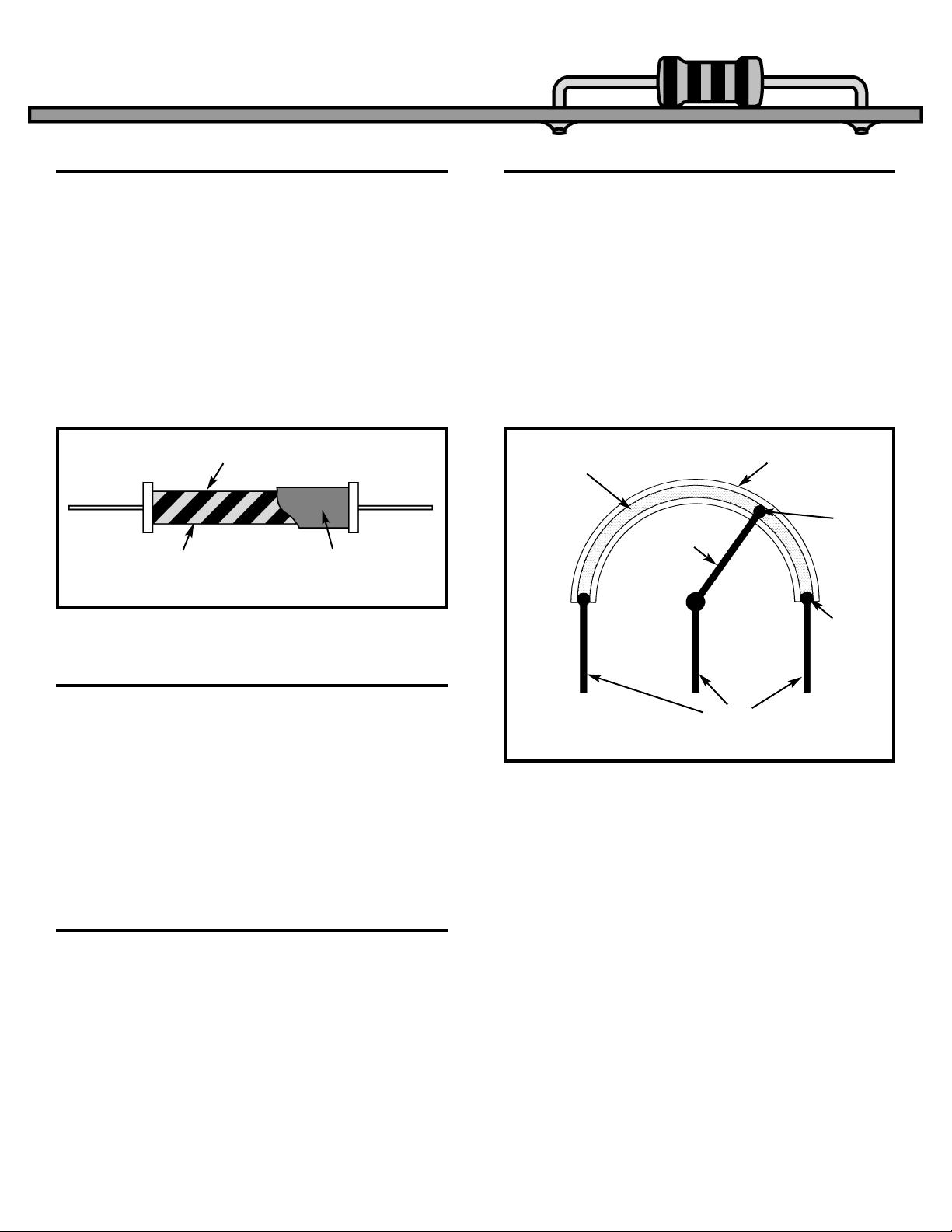
When a resistor is constructed so its value can be
adjusted, it is called a variable resistor. Figure 6
shows the basic elements present in all variable
resistors. First a resistive material is deposited on a
non-conducting base. Next, stationary contacts are
connected to each end of the resistive material.
Finally, a moving contact or wiper is constructed to
move along the resistive material and tap off the
desired resistance. There are many methods for
constructing variable resistors, but they all contain
these three basic principles.
Figure 5
METAL OXIDE RESISTORS
METAL FILM RESISTORS
THE VARIABLE RESISTOR
Figure 6
Carbon Film
Ceramic Rod Flameproof Jacket
Leads
Movable
Arm
Wiper
Contact
Stationary
Contact
Thin Layer
of Resistive
Material
Non-conductive
Base Material
Page 5

-4-
RESISTORS
RESISTOR VALUES AND MARKINGS
The unit of measure for resistance is the ohm, which
is represented by the Greek letter Ω. Before
technology improved the process of manufacturing
resistors, they were first made and then sorted. By
sorting the values into groups that represented a 5%
change in value, (resistor values are 10% apart),
certain preferred values became the standard for
the electronics industry. Table 1 shows the standard
values for 5% resistors.
Resistors are marked by using different colored
rings around their body (see Figure 7). The first ring
represents the first digit of the resistor’s value. The
second ring represents the second digit of the
resistor’s value. The third ring tells you the power of
ten to multiply by. The final and fourth ring
represents the tolerance. For example, gold is for
5% resistors and silver for 10% resistors. This
means the value of the resistor is guaranteed to be
within 5% or 10% of the value marked. The colors
in Table 2 are used to represent the numbers from 0
to 9.
Note: If the third ring is gold, you multiply the first
two digits by 0.1 and if it is silver, by 0.01. This
system can identify values from 0.1Ω to as high as
91 x 10
9
, or 91,000,000,000Ω. The amount of power
each resistor can handle is usually proportional to
the size of the resistor. Figure 8 shows the actual
size and power capacity of normal carbon film
resistors, and the symbols used to represent
resistors on schematics.
10 11 12 13 15 16 18 20
22 24 27 30 33 36 39 43
47 51 56 62 68 75 82 91
Table 1
Figure 7
OrangeRed
Violet Gold
27 X 103= 27,000 Ω,
with 5% Tolerance
COLOR VAL UE
Black 0
Brown 1
Red 2
Orange 3
Yellow 4
Green 5
Blue 6
Violet 7
Gray 8
White 9
Table 2
Figure 8
Regular Variable
Resistor Symbols
1/8 Watt
1/4 Watt
1/2 Watt
Page 6

-5-
RESISTORS
SELF TEST
1. A flow of electrons through a material:
a) Voltage c) Current
b) Resistance d) Conductance
2. The pressure that pushes electrons through a
material:
a) Voltage c) Conduction
b) Current d) Resistance
3. A material that has very high resistance to electron
flow:
a) Conductor c) Resistor
b) Semiconductor d) Insulator
4. A material that allows electrons to flow easily:
a) Conductor c) Resistor
b) Semiconductor d) Insulator
5. A material that produces electrical friction and
restricts the flow of electrons:
a) Conductor c) Resistor
b) Semiconductor d) Insulator
6. A resistor that is made by wrapping a wire around a
ceramic rod:
a) Carbon Film c) Thermistor
b) Carbon Composition d) Wirewound
7. A resistor made by heating powder and resin in an
oven:
a) Carbon Film c) Thermistor
b) Carbon Composition d) Wirewound
8. A resistor made by depositing a very thin layer of
resistive material on a ceramic rod:
a) Carbon Film c) Thermistor
b) Carbon Composition d) Wirewound
9. One of the preferred values for a 5% resistor:
a) 4000Ω c) 77Ω
b) 560Ω d) 395Ω
10. The amount of wattage a resistor can handle is
determined by:
a) Value c) Current
b) Voltage d) Size
THEORY
Circle the letter that best fits the description.
PRACTICE
Open the bag marked “resistors” and fill in the table below.
Color 1 Color 2 Color 3 Color 4 Value Percent Wattage
EXTRA CREDIT
Using a razor blade or sharp knife, scrape away the paint on the body of one resistor and determine the type of
construction used to make it. Try and determine all of the materials used including the metals used to make the
leads.
Page 7

-6-
CAPACITORS,
What do they do?
Capacitors are components that can store electrical
pressure (Voltage) for long periods of time. When a
capacitor has a difference in voltage (Electrical
Pressure) between its two leads it is said to be
charged. A capacitor is charged by forcing a one
way (DC) current to flow through it for a short period
of time. It can be discharged by letting an opposite
direction current flow out of the capacitor. Consider
for a moment the analogy of a water pipe that has a
rubber diaphragm sealing off each side of the pipe
as shown in Figure 9.
If the pipe had a plunger on one end, as shown in
Figure 9, and the plunger was pushed toward the
diaphragm, the water in the pipe would force the
rubber to stretch out until the force of the rubber
pushing back on the water was equal to the force of
the plunger. You could say the pipe is charged and
ready to push the plunger back. In fact, if the
plunger is released it will move back to its original
position. The pipe will then be discharged or with no
charge on the diaphragm.
Capacitors act the same as the pipe in Figure 9.
When a voltage (Electrical Pressure) is placed on
one lead with respect to the other lead, electrons are
forced to “pile up” on one of the capacitor’s plates
until the voltage pushing back is equal to the voltage
applied. The capacitor is then charged to the
voltage. If the two leads of that capacitor are
shorted, it would have the same effect as letting the
plunger in Figure 9 move freely. The capacitor
would rapidly discharge and the voltage across the
two leads would become zero (No Charge).
What would happen if the plunger in Figure 9 was
wiggled in and out many times each second? The
water in the pipe would be pushed by the diaphragm
then sucked back by the diaphragm. Since the
movement of the water (Current) is back and forth
(Alternating) it is called an Alternating Current or
AC. The capacitor will therefore pass an alternating
current with little resistance. When the push on the
plunger was only toward the diaphragm, the water
on the other end of the diaphragm moved just
enough to charge the pipe (transient current). Just
as the pipe blocked a direct push, a capacitor clocks
direct current (DC). An example of alternating
current is the 60 cycle (60 wiggles each second)
current produced when you plug something into a
wall outlet.
SUMMARY: A capacitor stores electrical energy
when charged by a DC source. It can pass
alternating current (AC), but blocks direct current
(DC) except for a very short charging current, called
transient current.
CAPACITORS
Pipe Filled with Water
Rubber Diaphragm
Sealing Center of Pipe
Plunger
Figure 9
Page 8

-7-
CAPACITORS,
How are they made?
There are many different types of capacitors used in
electronics. Each type is made from different
materials and with different methods. Capacitors
are also made to handle different amounts of
electrical pressure or voltage. Each capacitor is
marked to show the maximum voltage that it can
withstand without breaking down. All capacitors
contain the same fundamental parts, which consist
of two or more conductive plates separated by a
nonconductive material. The insulating material
between the plates is called the dielectric. The basic
elements necessary to build a capacitor are shown
in Figure 10.
Perhaps the most common form of capacitor is
constructed by tightly winding two foil metal plates
that are separated by sheets of paper or plastic as
shown in Figure 11. By picking the correct insulating
material the value of capacitance can be increased
greatly, but the maximum working voltage is usually
lowered. For this reason, capacitors are normally
identified by the type of material used as the
insulator or dielectric. Consider the water pipe with
the rubber diaphragm in the center of the pipe. The
diaphragm is equivalent to the dielectric in a
capacitor. If the rubber is made very soft, it will
stretch out and hold a large amount of water, but it
will break easily (large capacitance, but low working
voltage). If the rubber is made very stiff, it will not
stretch far, but will be able to withstand higher
pressure (low capacitance, but high working
voltage). By making the pipe larger and keeping the
stiff rubber we can achieve a device that holds a
large amount of water and withstands a high amount
of pressure (high capacitance, high working voltage,
large size). These three types of water pipes are
illustrated in Figure 12. The pipes follow the rule that
the capacity to hold water, (Capacitance) multiplied
by the amount of pressure they can take (Voltage)
determines the size of the pipe. In electronics the
CV product determines the capacitor size.
CAPACITORS
THE METAL FOIL CAPACITOR
Soft Rubber
Figure 12
Stiff Rubber
Stiff Rubber
Larger Size
Large Capacity
Low Pressure
Low Capacity
but can withstand
High Pressure
High Capacity and can withstand High Pressure
Figure 10
Lead 1
Nonconductive Material
Conductive Plate
Lead 2
Figure 11
Lead 1
Paper or Plastic Insulator
Conductive Foil
Lead 2
Page 9

-8-
DIELECTRIC CONSTANT,
What is it?
The dielectric (rubber diaphragm in the water pipe
analogy) in a capacitor is the material that can
withstand electrical pressure (Voltage) without
appreciable conduction (Current). When a voltage is
applied to a capacitor, energy in the form of an
electric charge is held by the dielectric. In the
rubber diaphragm analogy the rubber would stretch
out and hold the water back. The energy was stored
in the rubber. When the plunger is released the
rubber would release this energy and push the
plunger back toward its original position. If there
was no energy lost in the rubber diaphragm, all the
energy would be recovered and the plunger would
return to its original position. The only perfect
dielectric for a capacitor in which no conduction
occurs and from which all the stored energy may be
recovered is a perfect vacuum. The
DIELECTRIC
CONSTANT
(K) is the ratio by which the
capacitance is increased when another dielectric
replaces a vacuum between two plates. Table 3
shows the Dielectric Constant of various materials.
To make a variable capacitor, one set of stationary
aluminum plates are mounted to a frame with a
small space between each plate. Another set of
plates are mounted to a movable shaft and designed
to fit into the space of the fixed plates without
touching them. The insulator or dielectric in this type
of variable capacitor is air. When the movable plates
are completely inside the fixed plates, the device is
at minimum capacitance. The shape of the plates
can be designed to achieve the proper amount of
capacitance versus rotation for different
applications. An additional screw is added to
squeeze two insulated metal plates together
(Trimmer) and thus set the minimum amount of
capacitance.
CAPACITORS
Air, at normal pressure 1 Mica 7.5
Alcohol, ethyl (grain) 25 Paper, manila 1.5
Beeswax 1.86 Paraffin wax 2.25
Castor Oil 4.67 Porcelain 4.4
Glass flint density 4.5 10 Quartz 2
Glycerine 56 Water, distilled 81
Table 3
THE VARIABLE CAPACITOR
Figure 13
Fram e
Movable
Plates
Shaft
Fixed Plates
Trimmer
Page 10

The amount of charge a capacitor can hold
(capacitance) is measured in Farads. In practice,
one farad is a very large amount of capacitance,
making the most common term used micro-farad or
one millionth of a farad. There are three factors that
determine the capacitance that exist between two
conductive plates:
1. The bigger the plates are (Surface Area),
the higher the capacitance. Capacitance
(C) is directly proportional to Area (A).
2. The larger the distance is between the two
plates, the smaller the amount of
capacitance. Capacitance (C) is indirectly
proportional to distance (d).
3. The larger the value of the dielectric
constant, the more capacitance (Dielectric
constant is equivalent to softness of the
rubber in our pipe analogy). The
capacitance (C) is directly proportional to
the Dielectric Constant (K) of the insulating
material. From the above factors, the
formula for capacitance in Farads becomes:
C = 0.244K Picofarads *
C = Capacitance in Picofarads (Farad x 10
-12
)
K = Dielectric Constant
A = Area of one Plate in square inches
N = Number of Plates
d = Distance between plates in inches
Example Calculation for Capacitor shown in Figure 14.
C = 2.24 x (1 x 1)(2 - 1) / (.01) = 224 Picofarads or
0.000224 Microfarads.
* If A and d are in centimeters change 0.224 to
0.0885.
The older styles of capacitors were marked with
colored dots or rings similar to resistors. In recent
years, the advances in technology has made it
easier to print the value, working voltage, tolerance,
and temperature characteristics on the body of the
capacitors. Certain capacitors use a dielectric that
requires markings to insure one lead is always kept
at a higher voltage than the other lead. Figure 15
shows typical markings found on different types of
capacitors. Table 4 gives the standard values used
and the different methods for marking these values.
-9-
CAPACITANCE,
How is it calculated?
CAPACITORS
A(N-1)
d
Figure 14
0.01 inch
Glass K=10
1 inch
1 inch
CAPACITOR VALUES AND MARKINGS
Figure 15
B
682K
K
+10
+16V
2200μF 25V
10μF 25V
Radial
Electrolytic
Axial
Electrolytic
Disc
Tantalum
Electrolytic
Chip
(no
markings)
Page 11

-10-
CAPACITORS
Voltage
1
Code
2
Cap. Value3Typical Markings
4 5
Tolerance (%)
6
Markings
7
4 0G 100pF 100pF 101 +5% J
5.5 0L .001μF .001 102 +10% K
6.3 0J .015μF .015 152 +20% M
10 1A .002μF .002 202 –10% +30% Q
16 1C .0022μF .0022 222 –10% +50% T
25 1E .003μF .003 302 –20% +80% Z
35 1V .033μF .033 333 SPECIAL A
50 1H .047μF .047 473
63 1J .05μF .05 R05 Temperature
Markings
80 1K .068μF .068 R068
100 2A .1μF .1 104 NP0 {<10ppm / OC}
110 2Q .15μF .15 154 N100 {<100ppm / OC}
125 2B .2μF .2 204 N220 {<220ppm / OC}
160 2C 2.2μF 2.2 2R2 N820 {<820ppm / OC}
180 2Z 22μF 22 22 Y5F
200 2D 100μF 100 100 Y5T
220 2P 220μF 220 220 Y5V
250 2E 470μF 470 470 X5F
315 2F 1000μF 1000 1000 Z5U
Capacitor markings vary greatly from one
manufacturer to another as the above table shows.
Voltages may be marked directly (200V) or coded
(2D). The value of capacitance may be marked
directly on the part as shown in columns 4 and 5
(note that .001μF and 1000μF have the same
marking, but the difference in size makes the value
obvious). The number 102 may also be used to
represent 1000 (10+2 zeros). In some instances the
manufacturer may use an R to represent the
decimal point. The tolerance is usually printed
directly on the capacitors. When it is omitted, the
standard tolerance is assumed to be +80% to –20%
for electrolytics. Capacitance change with
temperature is coded in parts per million per degree
C, {N220 = 220/1,000,000 or .022%}, or by a
temperature graph. See manufacturers
specifications for complete details.
CAPACITOR SYMBOLS
Figure 16 shows the schematic symbols used to represent
capacitors. The + symbol indicates that the capacitor is
polarized and the lead marked with the + sign must always
have a
higher
voltage than the other lead. The curved
plate, plate with sides, and minus sign also indicate the
capacitor is polarized and these leads must always be at a
lower
voltage than the other lead. The arrow crossing
through the capacitor indicates of capacitance is variable.
Figure 16
+
–
Standard VariablePolarized
Page 12

-11-
CAPACITORS
SELF TEST
1. A flow of electrons in one direction:
a) AC Voltage c) Alternating Current
b) Direct Voltage d) Direct Current
2. When two conductive plates are moved closer
together Capacitance will:
a) Increase c) Stay the Same
b) Decrease d) Vary Downwards
3. The name given to the material between a capacitor’s
plates:
a) Air c) Conductor
b) Dielectric d) Insulator
4. Electrons flowing in and out of a wire:
a) AC Voltage c) Alternating Current
b) Direct Voltage d) Direct Current
5. If the size of the conductive plates is increased,
capacitance will:
a) Increase c) Stay the Same
b) Decrease d) Vary Downwards
6. A capacitor will block:
a) AC Voltage c) Alternating Current
b) Direct Voltage d) Direct Current
7. When electrons are forced onto one plate of a
capacitor:
a) Polarization c) Storage
b) Discharging a) Charging
8.
A capacitor lead that is marked with a + must always be:
a) Grounded c) At higher voltage than
the other lead
b) At highest voltage d) b & c
9. A small disc capacitor marked 100 has a value of:
a) 100μF c) 100pF
b) .00001F d) 100F
10. A large electrolytic capacitor marked 100 has a value
of:
a) 100μF c) 100pF
b) .00001F d) 100F
11. If a dielectric is changed from air to distilled water the
capacitance will:
a) remain the same c) decrease
b) increase 81 times d) drop in half
12. A dielectric that stores energy with no loss:
a) Does not exist c) Pure Glass
b) Air d) A perfect vacuum
THEORY
Circle the letter that best fits the description.
PRACTICE
Open the bag marked “capacitors” and fill in the table below.
EXTRA CREDIT
What happens to the total capacitance if you connect two
capacitors as shown in Figure 17. Hint, use water pipe
analogy and try to calculate equivalent if one water pipe.
Type Capacitance
Value
Working
Voltage
Polarized
(Y/N)
Other
Markings
Figure 17
10μF
20μF
? μF
Table 4
Page 13
-12-
INDUCTORS
INDUCTORS,
What do they do?
The electronic component known as the inductor is
best described as electrical momentum. In our
water pipe analogy the inductor would be equivalent
to a very long hose that is wrapped around itself
many times (see Figure 18). If the hose is very long
it will contain many gallons of water. When pressure
is applied to one end of the hose, the thousands of
gallons of water would not start to move instantly. It
would take time to get the water moving due to
inertia (a body at rest wants to stay at rest). After a
while the water would start to move and pick up
speed. The speed would increase until the friction of
the hose applied to the amount of pressure being
applied to the water. If you try to instantly stop the
water from moving by holding the plunger, the
momentum (a body in motion wants to stay in
motion) of the water would cause a large negative
pressure (Suction) that would pull the plunger from
your hands.
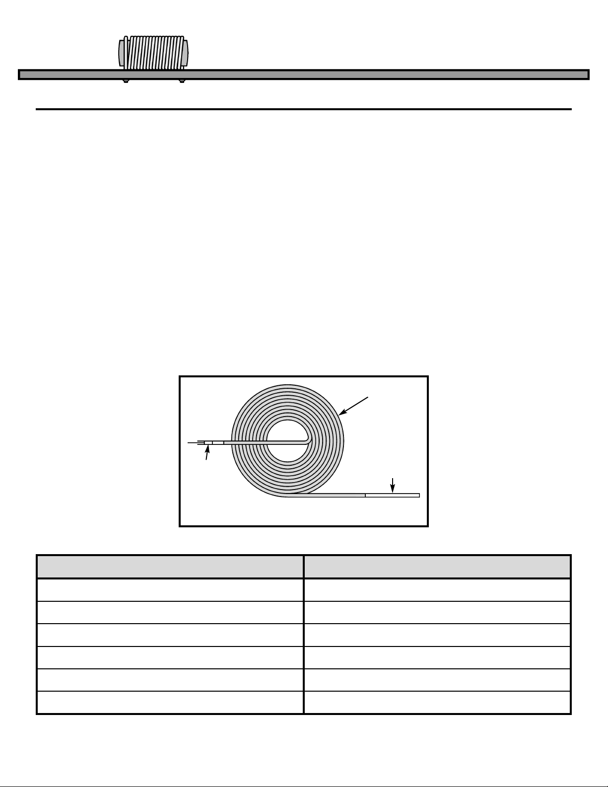
Since Inductors are made by coiling a wire, they are
often called Coils. In practice the names Inductor
and Coil are used interchangeably. From the above
analogy, it is obvious that a coiled hose will pass
Direct Current (DC), since the water flow increases
to equal the resistance in the coiled hose after an
elapsed period of time. If the pressure on the
plunger is alternated (pushed, then pulled) fast
enough, the water in the coil will never start moving
and the Alternating Current (AC) will be blocked.
The nature of a Coil in electronics follows the same
principles as the coiled hose analogy. A coil of wire
will pass DC and block AC. Recall that the nature of
a Capacitor blocked DC and passed AC, the exact
opposite of a coil. Because of this, the Capacitor
and Inductor are often called Dual Components.
Table 5 compares the properties of capacitors and
inductors.
Plunger
Water Pipe
Large Hose Filled
with Water
Figure 18
Capacitor Inductor
Blocks Direct Current Blocks Alternating Current
Passes Alternating Current Passes Direct Current
Voltage in Capacitor cannot change instantly Current in an Inductor cannot change instantly
Quick Voltage change produces large Current Quick Current change produces large Voltage
Stores Energy in Electric Field Stores Energy in Magnetic Field
Current leads Voltage Voltage leads Current
Table 5
Page 14

-13-
INDUCTORS,
How are they made?
In order to understand how inductors are made, we
have to change our water pipe analogy slightly to
include the effect of magnetic fields. Consider two
pipes filled with water and small magnets attached
to the walls of the pipes with rubber bands as shown
in Figure 19. The moving magnets, due to the
original current, pull the magnets in the second pipe
and force a small current to flow in the same
direction as the original current. When the rubber
bands are fully stretched, the induced current will
stop, even though the initial DC current is still
flowing. If the original current is an AC current
however, it will induce a continuous AC current in the
second pipe because the magnets will move back
and forth, pulling the magnets in the second pipe
back and forth.
Consider the two coiled pipes shown in Figure 20.
When the pipe is stretched out (increased length) as
in coil 1, the adjacent turns have little affect on each
other. In coil 2 (decreased length) the magnets in
each turn of the pipe are linking and the amount of
“apparent mass” in the pipe seems to increase. In
an inductor, pushing the coiled wire closer together
causes the inductance of the coil to also increase,
and stretching the coil out will lower the inductance
of the coil. In other words, the inductance of a coil
is indirectly proportional to its length. If the diameter
of the coil is increased, it will take more hose to form
a loop, and the amount of water will therefore
increase. More water means a larger “apparent
mass”. Inductance will also increase in a coil if the
cross sectional area increases. Inductance is
directly proportional to area.
Consider the affect of adding more turns to coiled
pipe. The amount of material to push (mass) is
increased and the amount of linkage is increased
due to more magnets available. This causes the
“apparent mass” to increase at a greater rate than
would be expected. When making an inductor, the
actual inductance is directly proportional to the
square of the number of turns.
The final factor to consider when making a coil is the
core material at the center of the coil. If our pipe
wrapped around a material that contained many
magnets, they would also link to the magnets in the
pipe. This would increase the “apparent mass” of
the water in the pipe.
The tiny magnets in
the core would rotate
as shown in Figure 21
and force the water to
keep moving in the
same direction.
Placing an iron core at
the center of an
inductor will directly
increase the
inductance by an
amount equal to the
permeability of the
core material.
INDUCTORS
Figure 20
Figure 21
Coil 1
Coil 2
Many tiny
magnets
IN
OUT
Figure 19
Induced
Current
Initial
Current
Page 15

-14-
INDUCTORS
INDUCTANCE,
How is it calculated?
Reviewing how coils are made will show the
following:
1. Inductance of a coil is indirectly proportional to
the length of the coil.
2. Inductance is directly proportional to the cross
sectional area.
3. Inductance is proportional to the square of the
number of turns.
4. Inductance is directly proportional to the
permeability of the core material.
From the above information the formula for
inductance of a simple iron core would be:
L =
Where:
L = Inductance in microhenrys
N = Number of turns
μ = Permeability of core material
A = Cross-sectional area of coil, in square inches
l = Length of coil in inches
This formula is good only for solid core coils with
length greater than diameter.
N
2
μA
10l
TRANSFORMERS,
How are they made?
Placing different coils on the same iron core as
shown in Figure 22 produces the electronic
component known as the Transformer. If a DC
current is forced through the center coil, the other
two coils will only produce a current when the
original current is changing. Once the DC current
reaches a constant value, the other two coils will
“unlink” and produce no flowing current if loaded. If
the generator voltage is continuously changing as in
Figure 22, it will produce a current that changes with
time. This changing current in the center coil will
produce similar currents in both of the end coils.
Since the bottom coil has twice the number of turns
(twice the magnetic linkage), the voltage across this
coil will be twice the generator voltage. The power
in an electronic device is equal to the voltage across
the device times the current through the device
(P=VI). If the voltage doubles on the bottom
winding, then the current must become 1/2 due to
the law of conservation of power (Power cannot be
created or destroyed, but can be transformed from
one state to another). Since the bottom coil is
wound in the same direction as the generator coil,
the voltage across the coil (top wire to bottom wire)
will be the same polarity as the generator voltage.
The top coil is wound in the opposite direction
forcing the core magnet rotation (Called flux by the
Pros) to push the current in the opposite direction
and produce a voltage of the opposite polarity.
Since the number of turns in the top coil are the
same as the generator coil, the voltage and current
(Power that can be taken from the coil) will also be
equal. This ability to transform AC voltages and AC
currents influenced early experimenters to call this
device a Transformer.
Figure 22
Voltage
Generator
Iron Core –V
Opposite
Voltage
i
i
½i
2V
2N Turns
N Turns
Direction of
Core Magnet
Rotation Due
to Current i
Page 16

-15-
TWO MORE LAWS ABOUT INDUCTORS
Faraday’s Law states that any time a conductor
moves through a magnetic field (Figure 23) a
voltage is generated. Because of this principle, it is
possible to attach a magnet (or coil) to a rotating
device and produce large amounts of electrical
power (the Hoover Dam for example).
Lenz’ Law states that the induced currents in a
conductor passing through a magnetic field will
produce a magnetic field that will oppose the motion
between the magnet and the conductor. To produce
a large amount of electrical power, a large
mechanical force is required (conservation of
power).
Most inductors are custom made to meet the
requirements of the purchaser. They are marked to
match the specification of the buyer and therefore
carry no standard markings. The schematic
symbols for coils and transformers are shown in
Figure 24. These symbols are the most commonly
used to represent fixed coils, variable coils, and
transformers.
The Q (figure of merit) of a coil is the ratio of the
inductive reactance to the internal series resistance
of the coil. Since the reactance and resistance can
both change with frequency, Q must be measured at
the desired frequency. Anything that will raise the
inductance without raising the series resistance will
increase the Q of the coil; for example, using an iron
core. Lowering the series resistance without
lowering the inductance will also raise the Q, more
turns of larger wire for example. Q is important
when the inductor is used in a resonant circuit to
block or select desired frequencies. The higher the
Q, the tighter the selection of frequencies become.
The Inductor prevents current from making any
sudden changes by producing large opposing
voltages. Magnetic coupling can be used to
transform voltages and currents, but power must
remain the same. Coils and transformers can be
used to select frequencies.
INDUCTORS
Figure 23
Wire
Lines of Flux
Motion of
Magnet
S
N
INDUCTANCE SYMBOLS AND MARKINGS
THE Q FACTOR IN COILS
SUMMARY
Figure 24
Fixed Coils Variable Coils
Iron Core
Transformer
Tunable Transformer
X
L
r
Page 17

-16-
SELF TEST
1. The inductor is best described as:
a) Induced Voltage c)
Electrical Storage Device
b) Long Wire d) Electrical Momentum
2. When wires in a coil are moved closer together, the
inductance will:
a) Increase c) Stay the Same
b) Decrease
3. Another word used to represent an inductor:
a) Wire c) Transformer
b) Coil d) Conductor
4. If the diameter of a coil is increased, the inductance
will:
a) Increase c) Stay the Same
b) Decrease
5. If the number of turns in a coil is decreased, the
inductance of that coil will:
a) Increase c) Stay the Same
b) Decrease
6. An inductor will block:
a) Alternating Voltage c) Alternating Current
b) Direct Voltage d) Direct Current
7. When an iron core is placed into the center of a coil,
the inductance will:
a) Increase c) Stay the Same
b) Decrease
8. If voltage in a transformer is stepped down, the current
will:
a) Increase c) Must Stay the Same
b) Decrease
9. When a conductor is moved through a magnetic field:
a) Power is created c) Magnetic field is
reduced
b) A voltage is d) a & c
generated on the wire.
10. The Q factor of a coil is equal to:
a) Wire quality c) Ratio of inductance
b) Ratio of reactance to resistance
to resistance
11. If windings on a straight rod are in the same direction,
the induced voltage will have:
a) Same amplitude c) Same polarity
b) Different amplitude d) Different polarity
12. An inductor stores energy in its:
a) Electric field c) Core
b) Magnetic field d) Wires
THEORY
Circle the letter that best fits the description.
PRACTICE
Using the coil supplied, answer the following questions.
EXTRA CREDIT
What happens to the total inductance if you connect two
coils as shown in Figure 25. Hint, remember the coiled
hose analogy and try to calculate equivalent if one coiled
hose.
Figure 25
10μH
? μH
INDUCTORS
(Hold the leads and peel the tape off).
Is the coil wound on an iron form? Yes ____ No ____
What prevents the wire from shorting? ________________________________________
How many turns are on the coil? _____________________
Example: Using a length of 0.1”, a radius of 0.02”, permeability of 14 for the iron core, and 56 turns, calculate
the inductance of the coil and record here: ________________________
20μH
Page 18

-17-
SEMICONDUCTORS
THE DIODE,
what is it?
The diode can be compared to the check valve
shown in Figure 26. The basic function of a check
valve is to allow water to flow in only one direction.
Once the force of the spring is exceeded, the plate
moves away from the stop allowing water to pass
through the pipe. A flow of water in the opposite
direction is blocked by the solid stop and plate. If it
took a pressure of 0.7lb to exceed the spring force,
the flow of water versus pressure might look like
Figure 27. In electronics, this curve would represent
the typical silicon diode if pounds per square inch
equaled volts and gallons per minute equaled
amperes. Of course, the amount of current that
flows through the diode must be limited or the device
could be damaged. Just as too much water through
the check valve could destroy the plate (shorted
diode). If the diode is made of Gallium Arsenide, it
would take approximately twice the voltage to
produce a flow of current (spring in Figure 26 is
twice as strong). The energy level required to “turn
on” a Gallium Arsenide diode is so high, that light is
generated when current starts to flow. These diodes
are called “Light Emitting Diodes”, or simply LED’s.
The transistor is best described as a device that
uses a small amount of current to control a large
amount of current (Current Amplifier). Consider a
device fabricated as shown in Figure 28. A small
amount of “Base Current” pushes on the L
1
portion
of the lever arm forcing check valve D
1
to open, even
though it is “reverse biased” (pressure is in direction
to keep check valve shut). Keep in mind the base
current would not start to flow until the check valve
D
2
allowed current to flow (0.7lb). If the current ratio
through D
1
and Base was equal to the lever arm
advantage, then I1/ Ib= L1/ L2. Call this ratio Beta
(β) and let L1= 1 inch and L2= 0.01 inch. Then β =
100 and I
1
will be 100 times Ib. Since both currents
must pass through D
2
, I2= I1+ Ib. These same
principles apply to a silicon NPN transistor. I
1
becomes collector current (IC), and I2would be
emitter current (I
E
). β = IC/ IBand IE= IB+ IC.
THE TRANSISTOR,
what is it?
Spring
Solid Stop
Movable Plate
Water-tight Pivot
Figure 26
Figure 27
0.7
Pressure (lbs per square inch)
Current (gals. per min.)
Figure 28
Base Current
I
b
L
1
L
2
I
1
D1
D2
I
2
Lever
Arm
NPN Transistor
Pivot
Page 19

-18-
SEMICONDUCTORS
THE PNP TRANSISTOR
Figure 29 represents the water pipe equivalent of a
PNP transistor. The emitter releases current that
splits into two paths. The base current “forces open”
the collector check valve which collects all the
current except the small amount that goes into the
base. The direction of current in the PNP transistor
is opposite that of the NPN transistor. Because of
these differences, the emitter of the PNP is usually
referenced to the power supply voltage and the
emitter of the NPN is usually referenced to ground
or zero voltage. In both transistors, the current
amplification factor (I
c/Ib
) is called Beta (β).
In Figure 30 the center of a small section of a pipe
is made of thin, flexible rubber and that rubber is
surrounded by water from a third pipe called the
gate. When pressure is applied to the gate, the
rubber pinches off the current from the source to the
drain. No current flows from gate to drain or source.
This device uses a change in gate pressure to
control the current flowing from source to drain.
Since there are no check valves, the current can
flow in either direction. In other words, this device
acts like a variable resistor. The Field Effect
Transistor (FET) also controls current between
source and drain by “pinching off” the path between
them. The level of voltage on the gate controls the
amount of current that will flow. Since no DC current
flows in or out of the gate (only momentarily a small
amount will flow to adjust to new pressures as in a
capacitor), the power used by the gate is very close
to zero. Remember, power equals voltage times
current, and if the current is zero, the power is zero.
This is why FET’s are used in the probes of test
equipment. They will not disturb the circuit being
tested by removing power during a measurement.
When a second gate section is added (pipe and
rubber) between the source and drain it is called a
Dual Gate FET. In our water pipe analogy of the
FET transistor, the rubber must be very thin and
flexible in order to “pinch off” the current from the
source to the drain. This means it could be easily
damaged by a small “spike” of high pressure. The
same is true of an electronic FET. A high voltage
“spike” (Static Electricity) can destroy the gate and
ruin the FET. To protect the FET, they are
sometimes packaged with metal rings shorting their
leads, and a fourth lead may be added to the metal
case containing the transistor.
Figure 29
Base
I
B
IE= IB+ I
C
PNP Transistor
THE FIELD EFFECT TRANSISTOR
Figure 30
Collector
Emitter
I
E
I
C
Drain
Source
Gate
FET Transistor
Page 20

-19-
SEMICONDUCTORS
THE INTEGRATED CIRCUIT
If the water pipe analogies of the resistor, diode,
transistor, and very small capacitors could be
etched into a single block of steel you would have
the equivalent of the Integrated Circuit in
Electronics. Figure 31 represents such a device.
This block of steel would have to be very large to
include all the mechanical parts needed. In
electronics, the actual size of a diode or transistor is
extremely small. In fact, millions can be fabricated
on a piece of silicon no larger than the head of a pin.
Photographic reduction techniques are used to
generate the masking needed to isolate each part.
These masks are then stepped and repeated in
order to make many separate integrated circuits at
the same time on a single substrate. Using mass
production techniques, these circuits are
manufactured, packaged, and sold at prices much
lower than the equivalent discreet circuit would cost.
SEMICONDUCTOR SYMBOLS
Figure 32 shows the common symbols used
in electronics to represent the basic
components. Integrated Circuits are usually
drawn as blocks with leads or as a triangle
for operational amplifiers. The Zener diode
(voltage reference diode) is used in the
reverse direction at the point of breakdown.
Figure 32
Diode LED
Zener
Diode
PNP NPN FET
Figure 31
The Integrated Circuit
8
7
14
1
Page 21

-20-
SEMICONDUCTORS
SELF TEST
1. The diode is best described as:
a) Switch c)
Electrical Storage Device
b) Check Valve d) Electrical Momentum
2. A silicon diode begins to conduct current at
approximately:
a) 7 volts c) 0.7 lb.
b) 0.7 volts d) 7 lbs.
3. NPN transistors have:
a) 2 leads c) 2 diodes
b) 3 leads d) b & c
4. NPN and PNP transistors are used to:
a) Create Power c) Control Current
b) Change Resistance d) Control Capacitance
5. The ratio of collector current to base current in a
transistor is called:
a) Beta (β) c) Current Control
b) Amplification d) FET
6. A diode made of Gallium Arsenide is called:
a) Zener Diode c) LED
b) Power Diode d) Detector Diode
7. A Field Effect Transistor controls Source to Drain
current by:
a) Diode Conduction c) Base Voltage
b) Base Current d) Gate Diode
8. A Zener Diode is used as:
a) Voltage Reference c) Resistance Control
b) Current Reference d) b & c
9. An Integrated Circuit contains:
a) Diodes and Resistors c) Inductors
b) Transistors and Small d) a & b
Capacitors
10. If the arrow in the symbol for a transistor points
toward the base lead, the transistor is a:
a) NPN Transistor c) FET Transistor
b) PNP Transistor
THEORY
Circle the letter that best fits the description.
PRACTICE
Open the Semiconductor bag and answer the following questions.
EXTRA CREDIT
Connect the LED (light emitting diode) to a 9 volt battery
(not provided) as shown in Figure 33. Why is the resistor
necessary? If the LED does not light up reverse the
battery leads. Why does the LED only light when
connected a certain way?
Figure 33
How many of the devices are diodes? __________
How many of the devices look like transistors? __________
How many integrated circuits are included? __________
Was a Light Emitting Diode included? __________
How are the diodes marked to show which end current will not go into? __________
Twisted
Leads
LED
1000Ω
Resistor
9V
Battery
Page 22

-21-
MECHANICAL PARTS
PRINTED CIRCUIT BOARDS,
What are they?
A printed circuit is a conductive pattern glued to one
or both sides of an insulating material. Holes are
punched or drilled through the conductor and board
to allow the interconnection of electronic parts. In
the case of a double sided board, the holes are
plated to provide a connection between the
conductors on both sides of the board. This method
provides considerable space savings over hand
wiring and allows for automated insertion and
soldering of parts. A more uniform product is
produced because wiring errors are eliminated. The
insulating material thickness may vary from 0.015”
to 0.500”. The most widely used base material is
NEMA-XXXP paper base phenolic. Copper is the
most common conductive material glued to the
base. The common thicknesses of the copper foil
are 0.0014” (1 oz./sq. ft.) and 0.0028” (2 oz./sq. ft.).
For single sided boards, the copper is laminated to
the board and then screened and etched away.
Double sided boards use a plating process and
conductive ink to achieve the desired layout.
Figure 34
Insulating
Material
Wrong
Copper
Correct
DESIGN RULES
After a the breadboard has been tested, there are
some design rules used to layout the printed circuit
board. A few of these basic rules are listed here:
1. Diameter of punched holes should not be less
than 2/3 the board thickness.
2. Distance between punched holes or between
holes and board edge should not be less than the
board thickness.
3. Holes should not exceed more than 0.020” of the
diameter of the wire to be inserted in the hole
(machine insertion may require more, but leads
should be “clinched”).
4. Conductor widths should be large enough to
carry current peaks. A width of one tenth of an
inch (1 oz./sq. ft. copper) will increase in
temperature 10
O
C at a DC current of 5A.
5. Conductor spacing must be capable of
withstanding applied voltages. If a voltage
difference of 500 volts exists between two copper
runs, they must be separated by at leads 0.03” to
prevent breakdown.
6. Avoid the use of sharp corners when laying out
copper (see Figure 34). Sharp corners produce
high electric fields that can lower breakdown.
Sharp corners will also make it easier for copper
to peel from the board.
7. Heavy parts must be mounted to prevent board
damage if the unit is dropped.
8. The printed circuit board must be fastened to
prevent leads from touching the case or any other
object mounted near the board.
9. Mounting hardware must be designed to prevent
board stress (warping or excessive torque).
Page 23

-22-
MECHANICAL PARTS
THE TOP LEGEND
The component side of a printed circuit board
should always have a drawing showing the
placement of the parts and their schematic marking
(R1, R2, etc.). This drawing is called the
To p
Legend
. When a board needs to be repaired, the
schematic becomes the “road map” and the top
legend becomes the “address” on the part. Figure
35 shows the correlation between the Schematic
and the Top Legend.
Different parts have been discussed. A printed
circuit board to interconnect these parts has been
discussed. Now it’s time to talk about the “Electronic
Glue” called Solder. Soldering wire is composed of
Tin and Copper with a rosin or acid core. Acid core
solder should never be used on electronic boards
since the acid will damage the components. Acid
core solder is mainly used to attach metals (copper
water pipes for example). When tin and copper are
mixed, the melting point of the mixture is lower than
the melting point of either tin or copper. The point at
which the melting point is the lowest is when the
mixture equals 99.3% tin and 0.7% copper. This is
called the eutectic (u tek’tik) point of the mixture.
The most common flux placed at the center of this
hollow wire alloy is Rosin based. Removing the flux
from the board requires a chemical that can dissolve
rosin. In recent years many water soluble fluxes
have been developed. These fluxes can be removed
by washing the boards in water.
After the parts are placed in the holes on the printed
circuit board, their leads should be trimmed and
bent. A good mechanical connection will improve
the soldering capability of the parts by forcing the
part and copper on the board to rise to the same
temperature. Positioning the soldering iron correctly
and using the right amount of heat are crucial to a
good solder job. Solder practicing is highly
recommended (Elenco
®
Solder Practice Kit Model
SP-1A).
SOLDER,
The Electronic Glue
Figure 35
Schematic
Printed Circuit Board
R1
C1
R2
B+
T1
D1
C2
Q1
R1
C1
R2
T1
D1
C2
Q1
Page 24

There are many other mechanical parts used by
manufacturers of electronic equipment. Most of
them fall into the category of switching or connecting
circuits. In Figure 36, five of the six parts shown are
used to switch or connect signals to the printed
circuit board. Only the spacer falls into a different
category, called mounting. The switch is used to
redirect current or voltage from one circuit to
another. The wire nut is used to hold two twisted
wires together and insulate them (prevent them from
being bare and exposed) at the same time. The PC
board male and female connectors are used to
attach wires from controls or other circuits to the
printed circuit board. The Earphone Jack is used to
bring a signal from the printed circuit board to an
earphone. The spacer holds the printed circuit
board away from the case to prevent leads from
shorting to the case.
There are many different methods for mounting
printed circuit boards. The simplest method is using
machine screws and spacers. Figure 37 shows
some of the common screw heads used by
electronic manufacturers. The oval head screw in
Figure 37 has a tapered end that will cut into the
metal and make a thread for the body of the screw.
The self-threading screw eliminates the need for a
nut and lockwasher but can produce metal
fragments that must be removed to prevent shorts
from occurring.
-23-
MECHANICAL PARTS
OTHER MECHANICAL PARTS
MOUNTING HARDWARE
Figure 37
Round Head
Pan Head
Fillister Head
Flat Head
Oval Head Self-threading
Figure 36
Switch
Wire Nut
Female Connector
Earphone Jack Female
Spacer
PC Board Male
Connector
Page 25

-24-
MECHANICAL PARTS
SELF TEST
1. Copper patterns on a Printed Circuit Board should
always be:
a) As thin as possible c) Rounded
b) Sharp and square d) On one side only
2. The distance between conductors on a printed circuit
should be large enough to:
a) Etch easily c) Clean
b) Solder across d) Prevent voltage
breakdown
3. The top legend shows:
a) Copper path c) Schematic
b) Part placement d) Hole numbers
4. The schematic shows:
a) Part placement c) Hole sizes
b) Copper path d)
Electrical connections
5. The material the copper is glued to on a printed circuit
board is called a:
a) Conductor c) Resistor
b) Semiconductor d) Insulator
6. Solder with the lowest melting point has a ratio of tin
to lead of:
a) 63/37 c) 40/60
b) 60/40 d) 37/63
7. Solder made for electronic parts has a:
a) Hollow Core c) Acid Core
b) Rosin Core d) No Core
8. The type of screw NOT mentioned in this course is:
a) Sheet Metal c) Round Head
b) Machine d) Self-threading
THEORY
Circle the letter that best fits the description.
PRACTICE
Open the Mechanical bag and answer the following questions.
EXTRA CREDIT
What is the function of the mechanical part(s) included in the bag that were not mentioned in the instruction
sheets?
How many of the following parts were in the mechanical bag?
Switches ______ Female PC Board Connectors ______ Male PC Board Connectors ______
Earphone Jacks ______ Wire Nuts ______ Spacers ______ Round Head Screws ______
Pan Head Screws ______ Flat Head Screws ______
Self-threading Screws ______ Sheet Metal Screws ______
Page 26

-25-
ANSWERS TO QUIZZES
PAGE 5
Type Capacitance Value Working Voltage Polarized (Y/N) Other Markings
Disc 33pF N —
Mylar .001μF 100 volts N K
Electrolytic 10μF 25 volts Y —
Electrolytic 220μF 25 volts Y —
Electrolytic 10μF 50 volts Y —
Electrolytic 10μF 16 volts Y —
Electrolytic 160μF 330 volts Y —
Answer to Extra Credit: 30μF
COLOR 1 COLOR 2 COLOR 3 COLOR 4 VALUE PERCENT WATTAGE
Brown Black Black Gold 10Ω 5% 1/2 Watt
Brown Green Brown Red 160Ω 5% 1/2 Watt
Brown Black Red Gold 1,000Ω 5% 1/4 Watt
Brown Red Red Gold 1,200Ω 5% 1/2 Watt
Red Yellow Red Gold 2,700Ω 5% 1/2 Watt
Brown Black Orange Gold 10,000Ω 5% 1/2 Watt
Blue Red Orange Gold 62,000Ω 5% 1/4 Watt
Red Black Green Gold 3,000,000Ω 5% 1/2 Watt
Green Brown Green Gold 5,100,000Ω 5% 1/4 Watt
Brown Black Blue Gold 10,000,000Ω 5% 1/2 Watt
1.c 2.a 3.d 4.a 5.c 6.d 7.b 8.a 9.b 10.d
PAGE 11
1.d 2.a 3.b 4.c 5.a 6.d 7.d 8.c 9.c 10.a 11.b 12.d
PAGE 16
1.d 2.a 3.b 4.a 5.b 6.c 7.a 8.a 9.b 10.b 11.c 12.b
Practice: No - the coil is not wound on a metal core. Enamel coating on wire prevents it from shorting.
There are 5 turns on the coil. Calculated inductance is 64 microhenrys.
Answer to Extra Credit: 30μH
PAGE 20
1.b 2.b 3.d 4.c 5.a 6.c 7.d 8.a 9.d 10.b
Practice: 3 Diodes 3 Transistors 1 Integrated Circuit Yes, 1 LED
A line is painted around the end that blocks current. LED uses flat side to indicate blocking end.
Answer to Extra Credit: Resistor is necessary to limit current and prevent LED from damage. LED’s are
diodes that only pass current in one direction.
PAGE 24
1.c 2.d 3.b 4.d 5.d 6.a 7.b 8.a
Practice: 1 Switch 1 Female 1 Male 1 Earphone Jack 1 Wire Nut 2 Spacers 1 Round 9 Pan
1 Flat Head 2 Self Threading 2 Sheet Metal
Answer to Extra Credit: Part in bag that was not mentioned included one strain relief to hold a line cord.
Parts included for further study were 2 thicknesses of rosin core solder and 1 printed circuit board. Using a
razor blade, slice solder on an angle to see internal flux.
Page 27

-26-
Space War Gun
K-10
Rapid fire or single shot with 2
flashing LEDs.
0-15V Power Supply
K-11
A low-cost way to supply
voltage to electronic games,
etc.
Christmas Tree
K-14
LED Robot Blinker
K-17
You’ll have fun displaying the PC
board robot.
Learn about
free-running
oscillators.
Digital Bird
K-19
You probably have never heard
a bird sing this way before.
Nerve Tester
K-20
Test your ability to
remain calm.
Indicates
failure by
a lit LED or
mild shock.
Yap Box
K-22A
This kit is a hit
at parties.
Makes 6
exciting
sounds.
Burglar Alarm
K-23
Alarm for your car, house, room,
or closet.
Whooper Alarm
K-24
Can be used as a
sounder or siren.
Metal Detector
K-26
Find new money and old
treasure. Get started in this
fascinating
hobby.
Pocket Dice
K-28
To be used with any game of
chance.
FM Microphone
AK-710/K-30
Learn about microphones,
audio amplifiers, and RF
oscillators. Range up
to 100 feet.
Telephone Bug
K-35
Our bug is only the size of a quarter,
yet transmits both sides of a
telephone conversation to any FM
radio.
Sound Activated Switch
K-36
Clap and the light comes on . . .
clap again and it goes off.
Lie Detector
K-44
The sound will tell
if you are lying.
The more you lie,
the louder the
sound gets.
Motion Detector
AK-510
Use as a sentry,
message
minder, burglar
alarm, or a
room
detector.
Two IC AM Radio
AM-780K
New design - easy-to-build,
complete radio on a single PC
board. Requires 9V battery.
Transistor Tester
DT-100K
Test in-circuit
transistors and
diodes.
Telephone Line Analyzer
TWT-1K
A telephone line analyzer kit
that tests active phone lines
with RJ-11 or RJ-45 modular
jacks.
Variable Power Supply
XP-720K
Three fully regulated supplies:
1.5-15V @ 1A, –1.5 to –15V @
1A or (3-30V @ 1A) and 5V @
3A.
EDUCATION KITS
Complete with PC Board and Instruction Book
Requires 9V battery
Requires
9V battery
Requires
9V battery
Requires 9V battery
Requires
9V battery
Requires
9V battery
Requires
9V battery
Requires
9V battery
Requires 2
“AA” batteries
Training course incl.
Requires
9V battery
Requires
9V battery
Requires
9V battery
Requires 9V battery
Produces flashing
colored LEDs
and three
popular
Christmas
melodies.
Requires
9V battery
No batteries required!
Requires
9V battery
0-15VDC @ 300mA
Page 28

ELENCO
®
150 Carpenter Avenue
Wheeling, IL 60090
(847) 541-3800
Website: www.elenco.com
e-mail: elenco@elenco.com
 Loading...