

Page 1
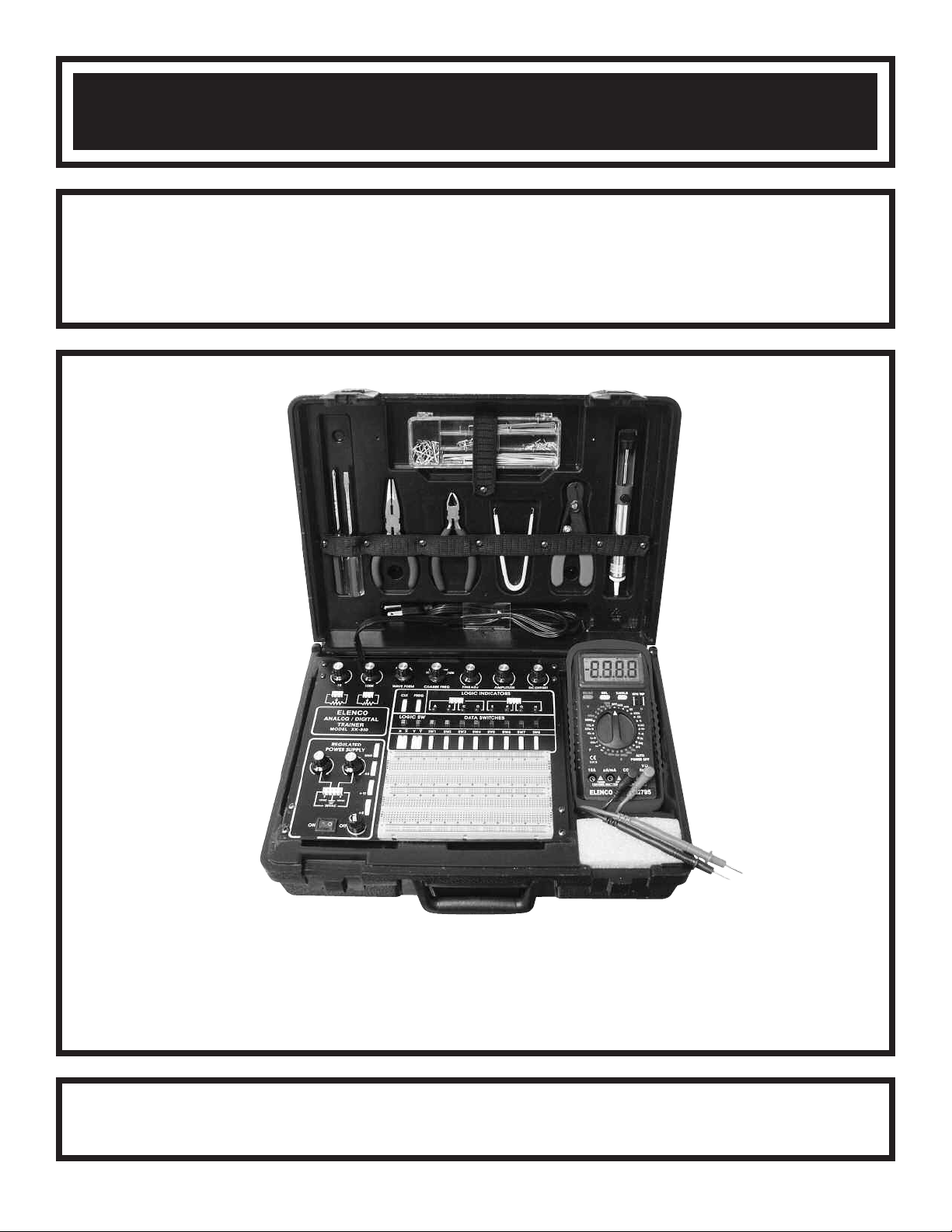
DIGITAL / ANALOG TRAINER
MODEL XK-550K
A COMPLETE MINI-LAB FOR BUILDING,TESTING
AND PROTOTYPING ANALOG AND DIGITAL CIRCUITS
Tools and meter shown not included.
Assembly & Instruction Manual
Elenco®Electronics, Inc.
Copyright © 2003, 1995 by Elenco®Electronics, Inc. All rights reserved. Revised 2003 REV-G 753550K
No part of this book shall be reproduced by any means; electronic, photocopying, or otherwise without written permission from the publisher.
Page 2
PS-550-B
XK-550K POWER SUPPLY KIT (PS-550-B) PARTS LIST
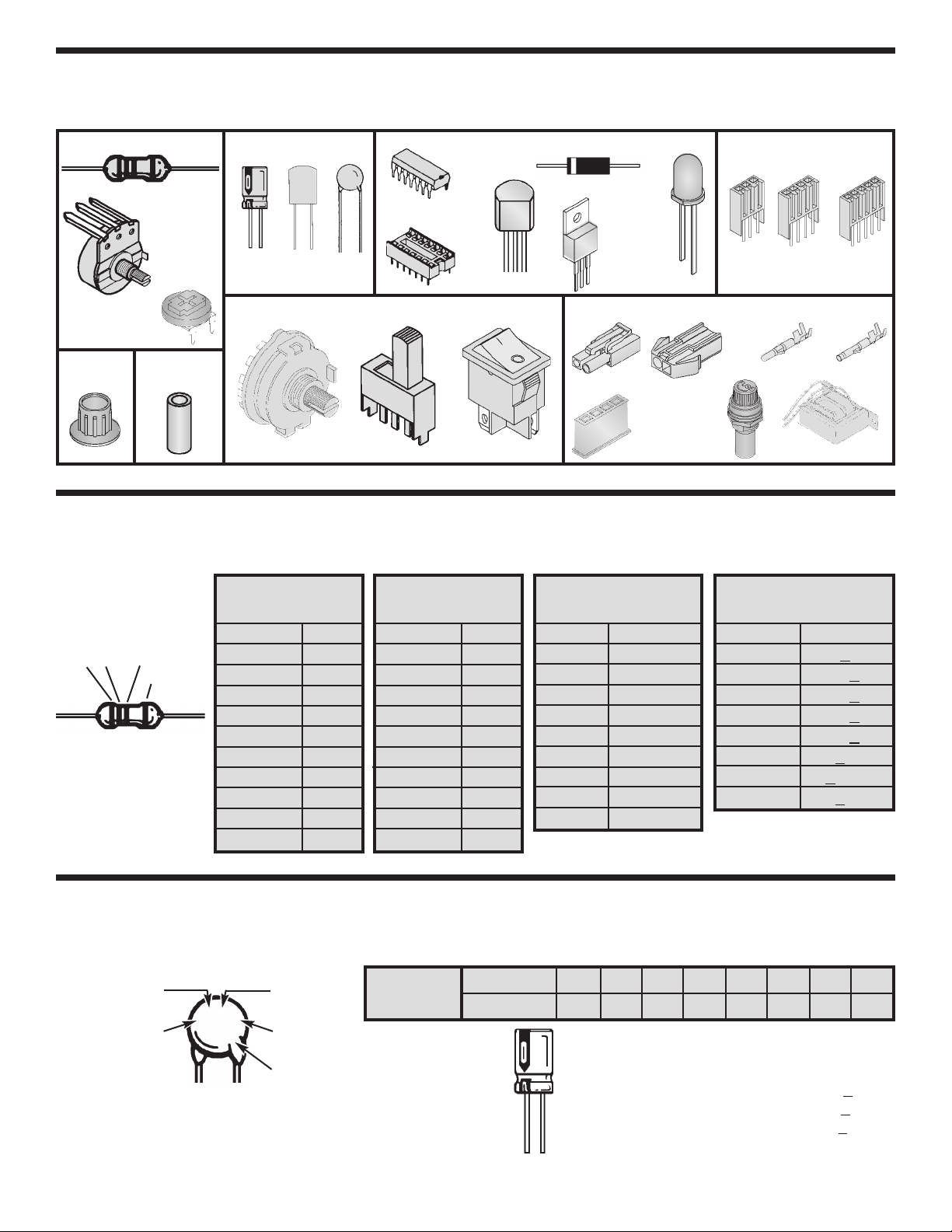
RESISTORS
QTY SYMBOL VALUE DESCRIPTION PART #
2 R1, R2 120Ω 5% 1/4W (brown-red-brown-gold) 131200
1 VR3 1KΩ Pot PC MNT 192412
2 VR1, VR2 2KΩ Pot PC MNT 192421
1 VR4 100KΩ Pot PC MNT 192612
CAPACITORS
QTY SYMBOL VALUE DESCRIPTION PART #
5 C6 - C10 .1µF 100V Mylar 251017
7 C11 - C17 100µF Electrolytic 281045
4 C1, C2, C4, C5 1000µF 35V Electrolytic 291096
1 C3 2200µF 25V Electrolytic 292225
SEMICONDUCTORS
QTY SYMBOL DESCRIPTION PART #
15 D1 - D15 1N4001 Diode 314001
1 U1 LM317 Integrated Circuit 330317
1 U5 LM337 Integrated Circuit 330337
1 U3 LM7805 Integrated Circuit 337805
1 U2 LM7812 Integrated Circuit 337812
1 U4 LM7912 Integrated Circuit 337912
MISCELLANEOUS
QTY DESCRIPTION PART #
1 Transformer 44K500
1 PC Board 514550
1 Fuse 1.25A 530125
1 Switch Illuminated 541204
2 Connector 3-pin 591032
1 Connector 5-pin 591052
1 Bracket 613003
4 Bracket L 4-40 tap 613008
1 Panel Top 614102
1 Panel Side Right 614551
1 Panel Side Left 614554
4 Knob 622009
1 Case 623002
1 Bushing 624009
1 Spacer Nylon 7/16” x 3/16” Tap 624013
1 Connector Receptacle 626020
1 Connector Plug 626021
1 Cord Retainer 628003
9 Screw 4-40 x 1/4” Slotted 641430
1 Screw 4-40 x 1/4” Phillips 641431
8 Screw 6-32 x 5/16” Slotted 641641
2 Screw 8-32 x 3/8” Phillips 641840
2 Screw #4 x 1/4” Phillips AB 642430
4 Screw #8 x 1/2” Phillips AB 642862
4 Screw #6 x 3/8” Phillips Thrd Ct 643652
Screw Identification
QTY DESCRIPTION PART #
4 Nut 7mm 644101
8 Nut 6-32 644601
2 Nut 8-32 644800
4 Washer 8mm x 14mm (Pot) 645101
4 Washer Fiber 645404
2 Lockwasher #6 INT 646600
2 Lockwasher #8 EXT 646828
1 Lug Solder #8 661002
1 Fuse Holder 663000
4 Bredblox 4-pin 665204
2 Terminal Male Crimp 666010
2 Terminal Female Crimp 666011
1 Label (XK-550K) 723501
1 Manual 753550K
5 Insulator Mica 780002
5 Insulator Washer 780101
1 Silicon Grease 790004
6” Wire #20 Red Stranded 813210
2.5’ Wire #22 Bare Wire 845000
1 Line Cord 862105
2” Shrink Tubing 3/16” 890120
1” Shrink Tubing 1/4” 890701
2” Shrink Tubing 1/2” 891101
2” Shrink Tubing 3/4” 899110
1 Solder Tube 9ST4A
(Type 23)
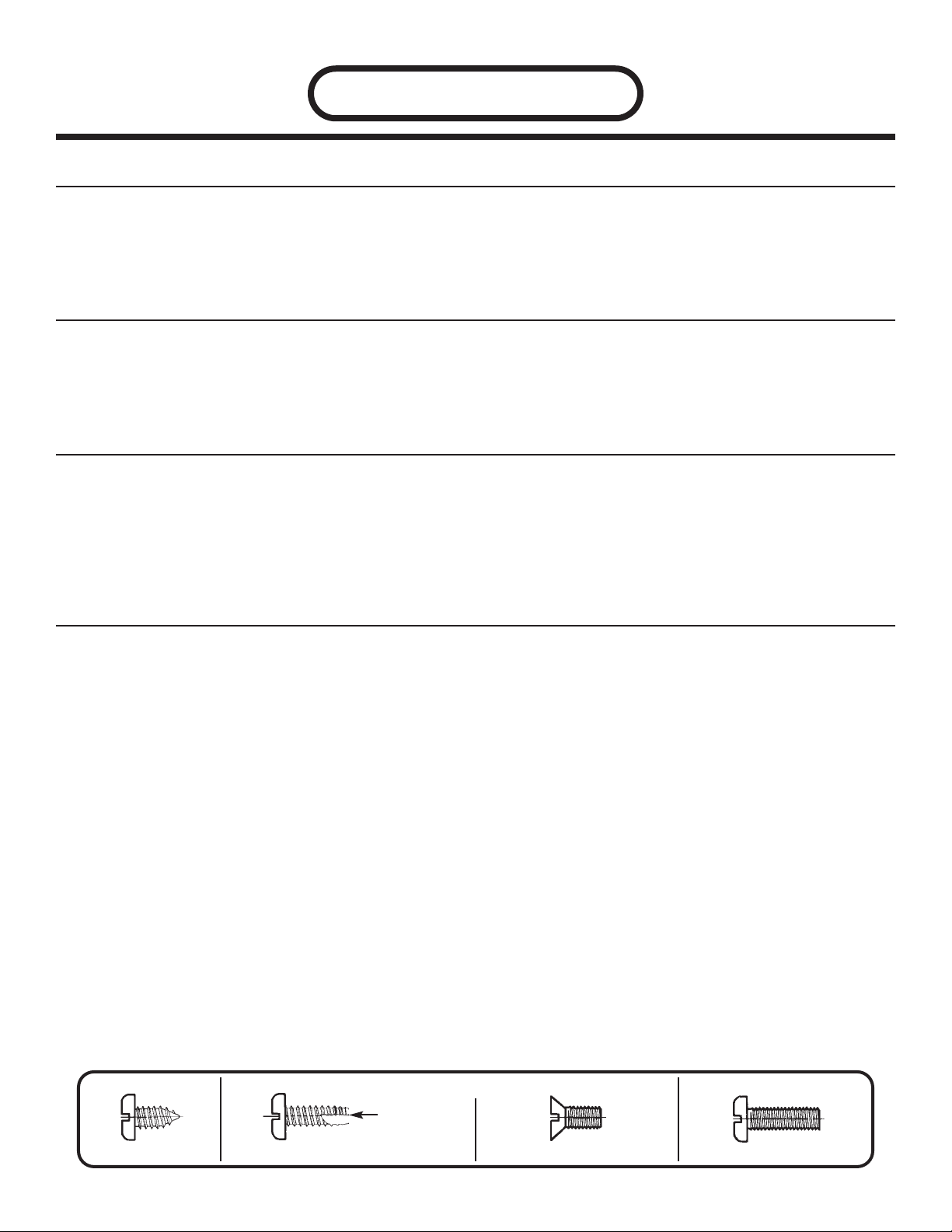
Phillips AB Screw 4-40 / #6 Thread Cutting Screw Standard Screw
Flat Head Screw
-1-
Page 3
PARTS VERIFICATION
efore beginning the assembly process, first familiarize yourself with the components and this instruction book.
B
Verify that all parts are present. This is done best by checking off each item in the parts list.
Resistors
Knob
C Mount
P
rim Pot
T
C Mount
P
Potentiometer
Spacer
Capacitors
Electrolytic
(
(Radial)
Mylar
Lytic)
otary DPDT
R
Discap
Switches
Integrated
Circuit (IC)
IC Socket
Semiconductors
Diode
ransistor
T
Connector Plug
lluminated
I
Integrated
Circuit (IC)
LED
Miscellaneous
Connector
Receptacle
IDENTIFYING RESISTOR VALUES
Use the following information as a guide in properly identifying the value of resistors.
Multiplier
Color Multiplier
Black 1
Brown 10
Red 100
Orange 1,000
Yellow 10,000
Green 100,000
Blue 1,000,000
Silver 0.01
Gold 0.1
Bands
1 2
Multiplier
Tolerance
BAND 1
1st Digit
Color Digit
Black 0
Brown 1
Red 2
Orange 3
Yellow 4
Green 5
Blue 6
Violet 7
Gray 8
White 9
BAND 2
2nd Digit
Color Digit
Black 0
Brown 1
Red 2
Orange 3
Yellow 4
Green 5
Blue 6
Violet 7
Gray 8
White 9
Connectors
Fuse
Assembly
3-Pin
4-Pin 5-Pin
ale Crimp
M
Terminal
Resistance
Tolerance
Color Tolerance
Silver +10%
Gold +5%
Brown +1%
Red +2%
Orange +3%
Green +0.5%
Blue +0.25%
Violet +0.1%
ransformerBredblox
T
Female Crimp
erminal
T
IDENTIFYING CAPACITOR VALUES
Capacitors will be identified by their capacitance value in pF (picofarads), nF (nanofarads), or µF (microfarads). Most
capacitors will have their actual value printed on them. Some capacitors may have their value printed in the following
manner. The maximum operating voltage may also be printed on the capacitor.
Second Digit
First Digit
The value is 10 x 1,000 =
10,000pF or .01µF 100V
103K
100V
Multiplier
Multiplier
Tolerance*
Maximum Working Voltage
For the No. 01234589
Multiply By 1 10 100 1k 10k 100k .01 0.1
10µF 16V
Note: The letter “R” may be used at times to
signify a decimal point; as in 3R3 = 3.3
*
The letter M indicates a tolerance of +20%
The letter K indicates a tolerance of +10%
The letter J indicates a tolerance of +5%
-2-
Page 4
CONSTRUCTION
Introduction
The most important factor in assembling your XK-550K Digital / Analog Trainer Kit is good soldering techniques.
Using the proper soldering iron is of prime importance. A small pencil type soldering iron of 25 - 40 watts is
recommended.The tip of the iron must be kept clean at all times and well tinned.
Safety Procedures
• Wear eye protection when soldering.
•
Locate soldering iron in an area where you do not have to go around it or reach over it.
• Do not hold solder in your mouth. Solder contains lead and is a toxic substance. Wash your hands
thoroughly after handling solder.
• Be sure that there is adequate ventilation present.
Assemble Components
In all of the following assembly steps, the components must be installed on the top side of the PC board unless
otherwise indicated. The top legend shows where each component goes. The leads pass through the
corresponding holes in the board and are soldered on the foil side.
Use only rosin core solder of 63/37 alloy.
DO NOT USE ACID CORE SOLDER!
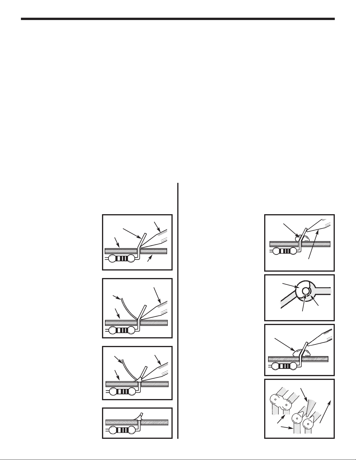
What Good Soldering Looks Like
A good solder connection should be bright, shiny,
smooth, and uniformly flowed over all surfaces.
1. Solder all components from
the copper foil side only.
Push the soldering iron tip
against both the lead and
the circuit board foil.
2. Apply a small amount of
solder to the iron tip. This
allows the heat to leave the
iron and onto the foil.
Immediately apply solder to
the opposite side of the
connection, away from the
iron. Allow the heated
component and the circuit
foil to melt the solder.
3. Allow the solder to flow
around the connection.
Then, remove the solder
and the iron and let the
connection cool. The
solder should have flowed
smoothly and not lump
around the wire lead.
4.
Here is what a good solder
connection looks like.
Component Lead
Foil
Solder
Foil
Solder
Foil
Soldering Iron
Circuit Board
Soldering Iron
Soldering Iron
Types of Poor Soldering Connections
1. Insufficient heat - the
solder will not flow onto the
lead as shown.
2. Insufficient solder - let the
solder flow over the
connection until it is
covered. Use just enough
solder to cover the
connection.
3. Excessive solder - could
make connections that you
did not intend to between
adjacent foil areas or
terminals.
4. Solder bridges - occur
when solder runs between
circuit paths and creates a
short circuit. This is usually
caused by using too much
solder. To correct this,
simply drag your soldering
iron across the solder
bridge as shown.
Rosin
Soldering iron positioned
incorrectly.
Solder
Component Lead
Solder
Soldering Iron
Foil
Gap
Drag
-3-
Page 5
INTRODUCTION
The XK-550K Digital/Analog Trainer is divided into four separate kits: BB-550-A, PS-550-B, AN-550-C and DG550D. Each bag of parts is clearly identified. Open only the kit called for in your procedure. DO NOT open any
other bag at this time. The first kit is the BB-550-A which contains only the bredboard. The bredboard will be
assembled to the front panel of the trainer during the assembly of the PS-550-B Power Supply. Read your
instructions carefully.
Power Supply
The XK-550K has five built-in power supplies which will satify most design needs. This includes two variable
power supplies giving up to +20 volts and –20 volts at .5 amp. Below 15V, the current availableis 1 amp. Three
fixed power supplies give you +12VDC, –12VDC or +5VDC at 1 amp each. These fixed voltages are the most
commonly used voltages for design work. All supplies are regulated to within 150mV. This means that you can
increase the current draw from no load to 0.5 amp and the voltage will change less than 150mV. All supplies
are also short circuit protected by using integrated circuit regulator devices.
Analog Trainer Section Function Generator
The analog trainer contains a complete function generator capable of producing sine, square and triangle
waveforms. The frequency of the generator is continuously variable from one hertz to over 100,000 hertz in five
steps. A fine tuning control makes the selection of any frequency easy. The output voltage amplitude is variable
between 0 to 15Vpp. The output impedance is approximately 330 ohms.
Digital Trainer Section
The digital trainer has the necessary functions to do your digital experiments. They consist of a clock generator,
two no-bounce switches, eight LED indicator lamps and eight data switches.
POWER SUPPLY SPECIFICATIONS
Power Supplies:
• +1.25V to 20VDC @ 0.5 amp (1.25V to 15V @ 1 amp).
• –1.25 to -20VDC @ 0.5 amp (–1.25V to –15V @ 1 amp).
• +12V +5% @ 1 amp.
• –12V +5% @ 1 amp.
• +5V +5% @ 1 amp.
• 30VAC center tapped @ 1 amp.
• Load regulation - all DC supplies less than 0.2V no load to 0.5A.
• Line regulation - all DC supplies less than0.2V 105 to 135V.
• Hum and ripple - all DC supplies less than 0.01V RMS.
• Short protection - all DC supplies-internal IC thermal cutoff.
• Fuse 1.25A 250V.
Variable Resistance (undedicated):
• 1kΩ Potentiometer
• 100kΩ Potentiometer
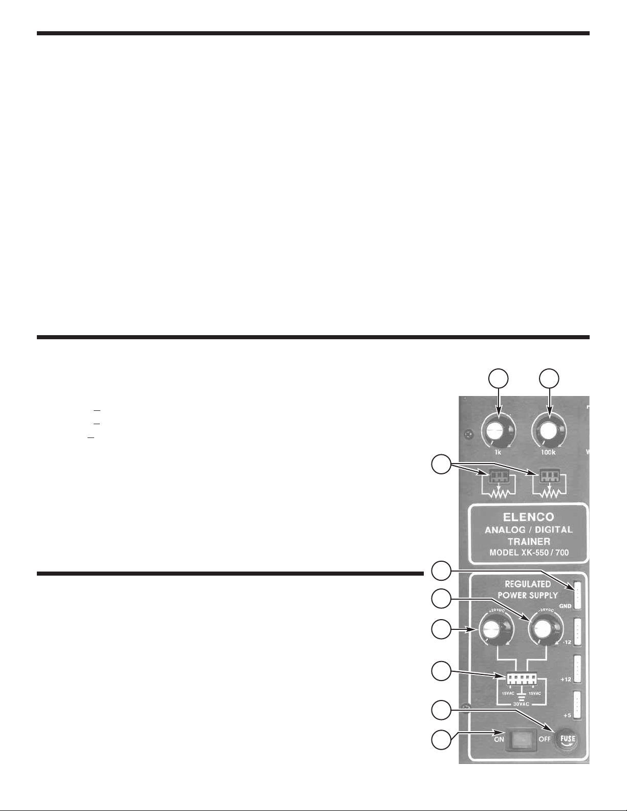
USERS DESCRIPTION OF FRONT PANEL CONTROLS
1) On/Off Switch - Allows power to be applied to all outputs. Switch will
light when on.
2) Fuse Holder - Easy access for replacement of 1.25A fuse.
3) Power Output Terminals - This provides 30VAC center tapped at
15 VAC; also provides output terminal for positive and negative
variable voltages.
4) Variable PositiveVoltage Control - Varies positive voltage from 1.25
to 20V at indicated output connector pin.
5) Variable Negative Voltage Control - Varies negative voltage from
–1.25V to –20V at indicated output connector pin.
6) Power Output Bredblox - Output terminals for GND, –12, +12, and +5.
7) Output terminals for 1k and 100k undedicated potentiometers.
8) 1kΩ undedicated potentiometer.
9) 100kΩ undedicated potentiometer.
8 9
7
6
5
4
3
2
1
-4-
Page 6
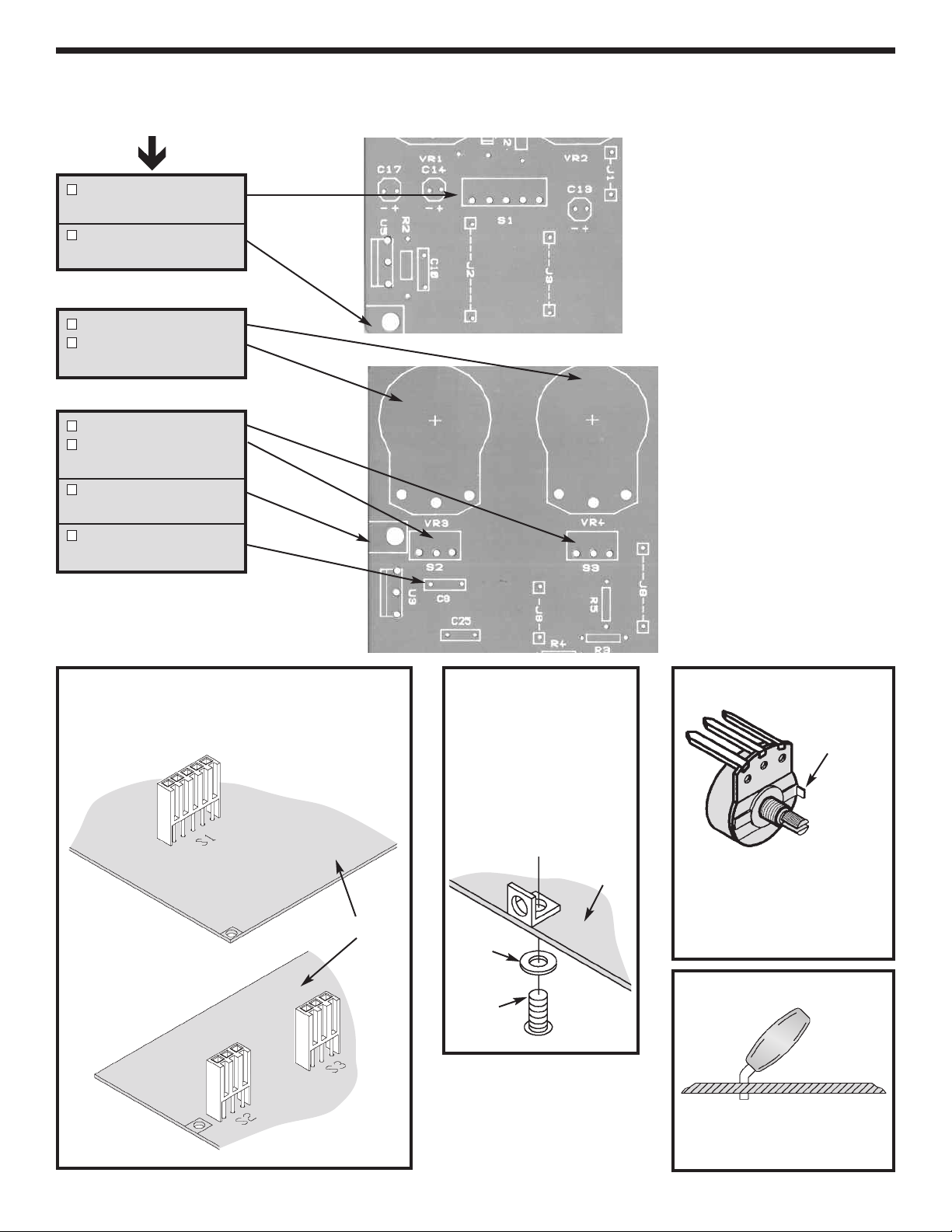
INSTALL COMPONENTS TO PC BOARD
Start Here
S1 - 5-Pin Connector
(see Figure A)
L-Bracket
(see Figure B)
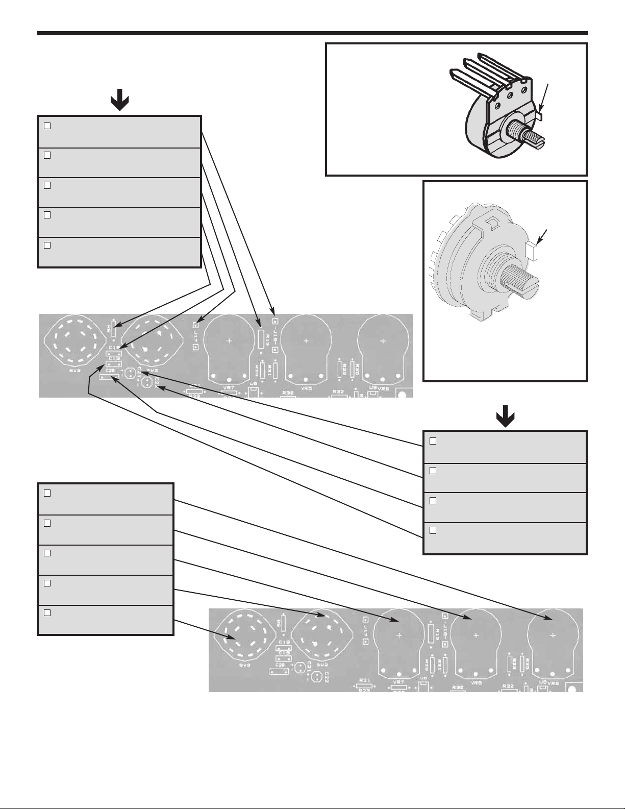
VR4 - 100kΩ Pot
VR3 - 1kΩ Pot
(see Figure C)
S3 - 3-Pin Connector
S2 - 3-Pin Connector
(see Figure A)
L-Bracket
(see Figure B)
C8 - 0.1µF Mylar (104)
(see Figure D)
Bottom Left Corner of PC Board
Top Left Corner of PC Board
Figure A
Mount the connector as shown and solder the
pins of the connector.
PC Board
Figure B
Note: One side of the
bracket is longer. Mount
this side to the PC board.
Mount the bracket to the
top legend side of the PC
board with a 4-40 x 1/4”
screw and fiber washer.
Top Legend
Side of
PC Board
Fiber
Washer
4-40 x 1/4”
Screw
Figure C
Cut off tab
Mount down flush withPCboard. The
value may be marked on the on the
back side of pot.
Cut off excess lead length after
soldering.
Figure D
Bend the capacitor at a 45
angle before soldering. Cut off
excess leads.
O
-5-
Page 7
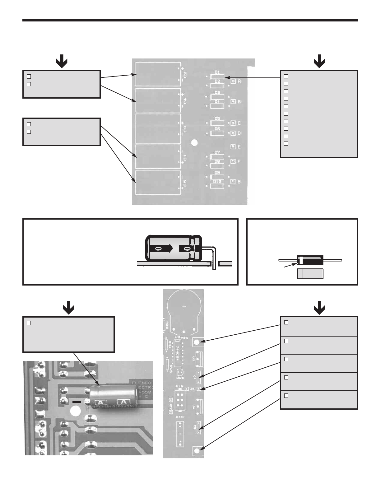
INSTALL COMPONENTS TO PC BOARD
Start Here
C11 - 100µF 25V
(see Figure E)
R1 - 120Ω 5% 1/4W Resistor
(brown-red-brown-gold)
C6 - .1µF Mylar (104)
(see Figure D)
J28 - Jumper Wire
(see Figure F)
J6 - Jumper Wire
(see Figure F)
D12 - 1N4001 Diode
D11 - 1N4001 Diode
(see Figure G)
C14 - 100µF 25V Lytic
C17 - 100µF 25V Lytic
(see Figure E)
C10 - .1µF Mylar (104)
(see Figure D)
Bottom Left Corner of PC Board
R2 - 120Ω 5% 1/4W Resistor
(brown-red-brown-gold)
J2 - Jumper Wire
(see Figure F)
J3 - Jumper Wire
(see Figure F)
These capacitors are polarized. Be
sure to mount them with the “+”
lead in the correct hole as marked
on the PC board. Mount the
capacitor lying flat on the PC board
as shown below.
Figure E
(–)
Figure F
Cut a piece of the #22 bare wire
long enough so that 1/4” of wire
passes through each hole in the
PC board after the wire is formed.
(+)
Figure G
Diodes have polarity. Mount them
with the band as shown on the top
legend.
-6-
Band
Page 8
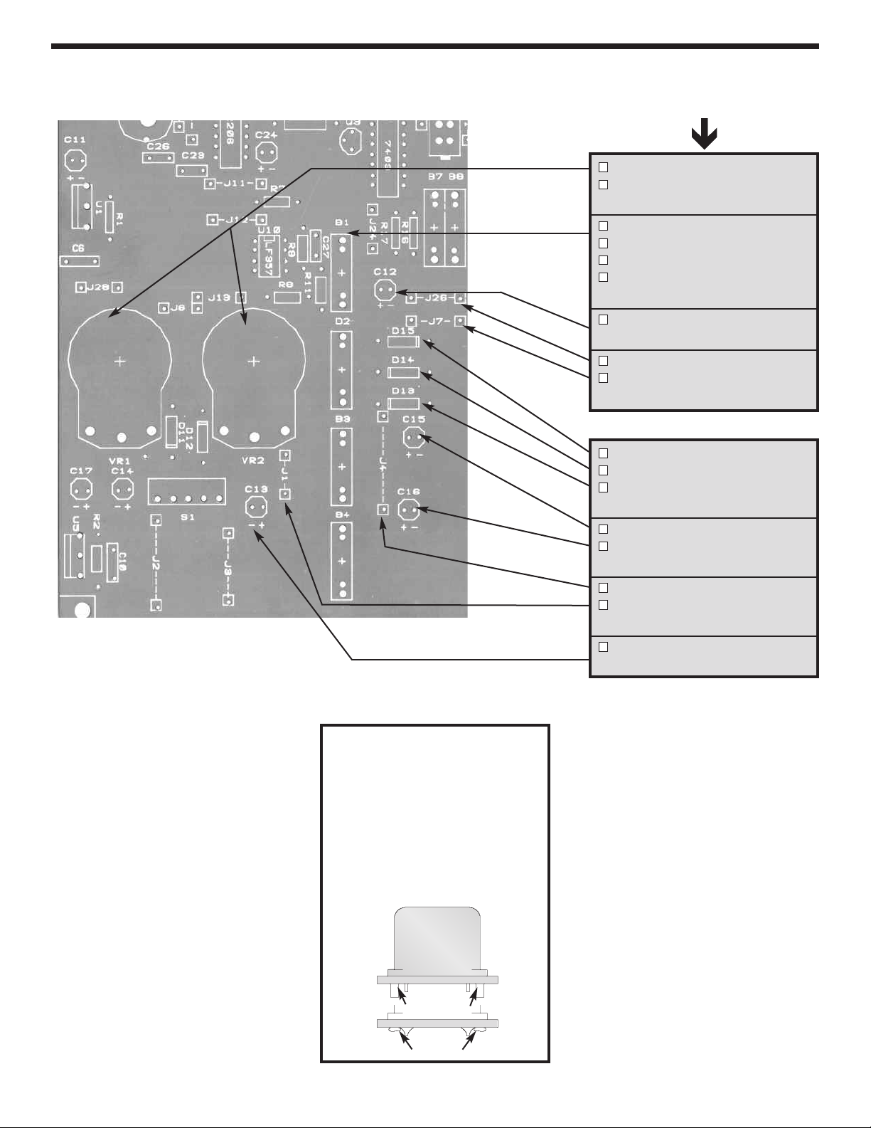
INSTALL COMPONENTS TO PC BOARD
Start Here
VR1 - 2kΩ Pot
VR2 - 2kΩ Pot
(see Figure C)
B1 - 4-Pin Bredblox
B2 - 4-Pin Bredblox
B3 - 4-Pin Bredblox
B4 - 4-Pin Bredblox
(see Figure H)
C12 - 100µF 25V Lytic
(see Figure E)
J26 - Jumper Wire
J7 - Jumper Wire
(see Figure F)
D15 - 1N4001 Diode
D14 - 1N4001 Diode
D13 - 1N4001 Diode
(see Figure G)
Bottom Left Corner of PC Board
C15 - 100µF 25V Lytic
C16 - 100µF 25V Lytic
(see Figure E)
J4 - Jumper Wire
J1 - Jumper Wire
(see Figure F)
C13 - 100µF 25V Lytic
(see Figure E)
Figure H
Hold the bredblock down flush
to the PC board from the top
legend side and solder the
metal pins in place. Then, melt
the plastic pins with your
soldering iron to hold the
plastic blocks in place, as
shown.
Plastic Pins
Melt Pins
-7-
Page 9
INSTALL COMPONENTS TO PC BOARD
Start Here Continue
C2 - 1000µF 35V Lytic
C4 - 1000µF 35V Lytic
(see Figure J)
C1 - 1,000µF 35V Lytic
C5 - 1,000µF 35V Lytic
(see Figure J)
Figure J
These lytics must be mounted
horizontal to the PC board. Bend
the leads at right angles and then
insert the leads into the PC board
with the negative (–) lead and the
positive (+) lead in the correct holes
as marked on the PC board.
Bottom Right Corner of PC Board
D1 - 1N4001 Diode
D2 - 1N4001 Diode
D3 - 1N4001 Diode
D4 - 1N4001 Diode
D5 - 1N4001 Diode
D6 - 1N4001 Diode
D7 - 1N4001 Diode
D8 - 1N4001 Diode
D9 - 1N4001 Diode
D10 - 1N4001 Diode
(see Figure I)
Figure I
Diodes have polarity. Mount them with
the band as shown on the top legend.
Band
Start Here
C3 - 2200µF Lytic
Mount on foil side of PC board
Note the polarity
(see Figure J)
+
-8-
Top Right Corner
of PC Board
Continue
L-Bracket
(see Figure B)
C7 - .1µF Mylar (104)
(see Figure D)
J5 - Jumper Wire *
(see Figure F)
C9 - .1µF (104) Mylar
(see Figure D)
L-Bracket
(see Figure B)
* Leftover wire will be used in
future sections.
Page 10
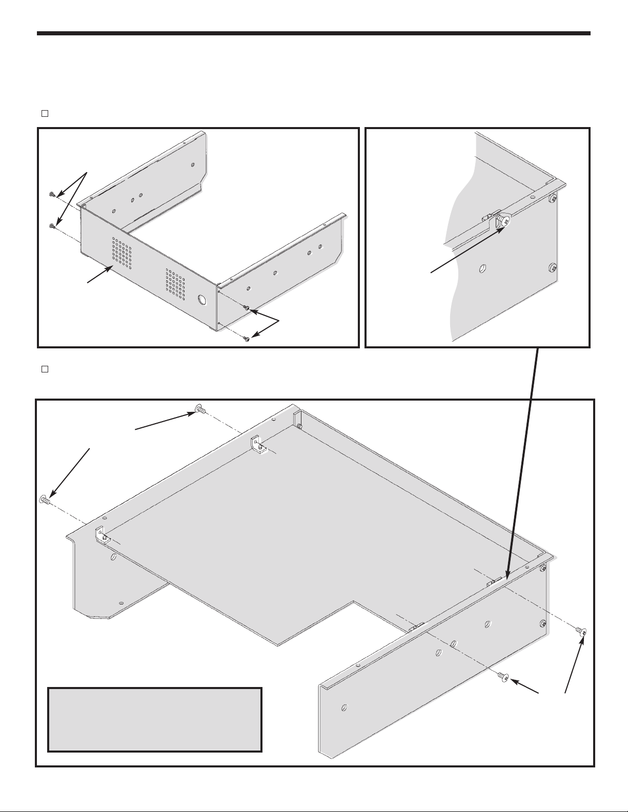
MOUNTING THE PC BOARD
Note: The holes in the two side panels have been punched differently. Be sure that you have the correct side
panel when mounting them to the PC board.
IMPORTANT: Push the PC board up as far as possible before tightening the screws, as shown in Figure La.
Mount the back panel using four 4-40 x 1/4” thread cutting screws (see Figure K).
4-40 x 1/4” Thread
Cutting Screws
Right Side
Left Side
Adjust the PC board
Back Panel
4-40 x 1/4” Thread
Figure K
Cutting Screws
Mount the PC board to the side panels with four 4-40 x 1/4” screws (see Figure L).
Do not tighten the screws.
4-40 x 1/4”
Machine Screws
height with a 4-40 x
1/4” screw
Left Side
Note: From the foil side of the PC board,
inspect the edges to be sure that there
are no component leads shorting against
the side panels.
Top Legend Side
of PC Board
-9-
Right Side
4-40 x 1/4”
Machine Screws
Figure L
Page 11
Place the top panel onto the unit and align the components with the holes in the top panel. Push the PC board up until
the components come through the top panel and tighten the screws.
Figure La
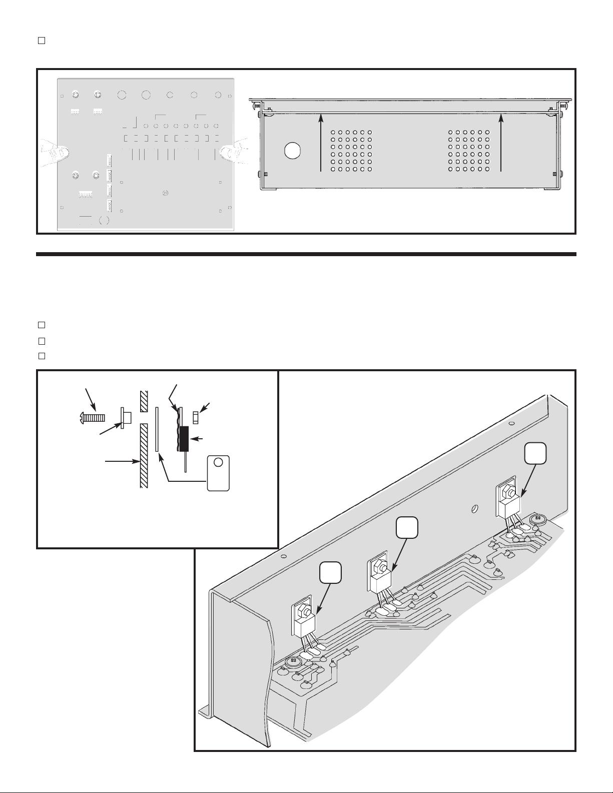
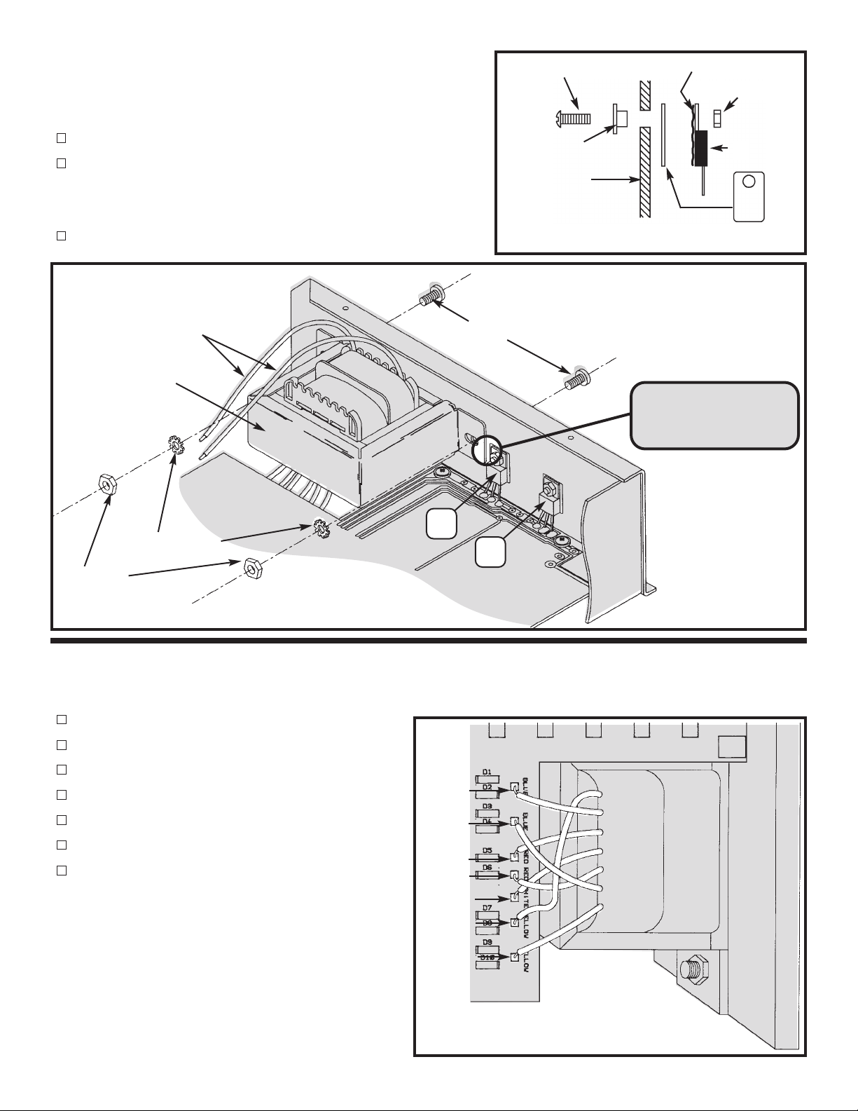
MOUNT COMPONENTS TOTHE SIDE PANELS
Mount U1, U3 and U5 to the left side panel as shown in Figure N. Insert the pins of each IC into the holes of
the PC board. Then, with the hardware shown in Figure M, attach each IC to the side panel. Solder the pins
of the ICs to the PC board.
U3 - LM7805
U1 - LM317
U5 - LM337
6-32 x 5/16” Screw
Insulator Washer
Side Panel
* Take a small amount of silicone grease from the
packet and apply it with a toothpick onto the back of
the ICs.
* Silicone Grease
6-23 Nut
IC
Mica
Figure M
U3
7805
U1
LM317
Left Side
U5
LM337
-10-
Figure N
Page 12
ount U2 and U4 to the right side panel as shown in Figure O.
M
Insert the pins of each IC into the holes in the PC board. Then,
with the hardware shown in Figure MA, attach each IC to the
side panel. Solder the pins of the ICs to the PC board.
6-32 x 5/16” Screw
* Silicone Grease
6-23 Nut
U4 - LM7912
U2 - LM7812
Mount the transformer with the black wires as shown in Figure O.
Use the two 8-32 x 3/8” screws, #8 lockwashers, and 8-32 nuts.
Transformer mounted
Figure O
Black Wires
Transformer
#8 Lockwashers
8-32 Nuts
#8-32 x 3/8” Screws
U4
7912
Insulator Washer
Side Panel
IC
Figure MA
*Take asmallamount of silicone grease fromthepacket and
apply it with a toothpick onto the back of the ICs.
Note: Make sure that
the transformer does
not touch U4.
Right Side
U2
7812
Mica
WIRE THE TRANSFORMER TOTHE PC BOARD
Solder the wires to the PC board starting with the top yellow wire as shown in Figure P.
Yellow wire to point F on the PC board
Blue wire to point A on the PC board
Red wire to point C on the PC board
White wire to point E on the PC board
Red wire to point D on the PC board
Blue wire to point B on the PC board
Yellow wire to point G on the PC board
Blue (A)
Blue (B)
Red (C)
Red (D)
White (E)
Yellow (F)
Yellow (G)
Figure P
Yellow (F)
Blue (A)
Red (C)
White (E)
Red (D)
Blue (B)
Yellow (G)
-11-
Page 13
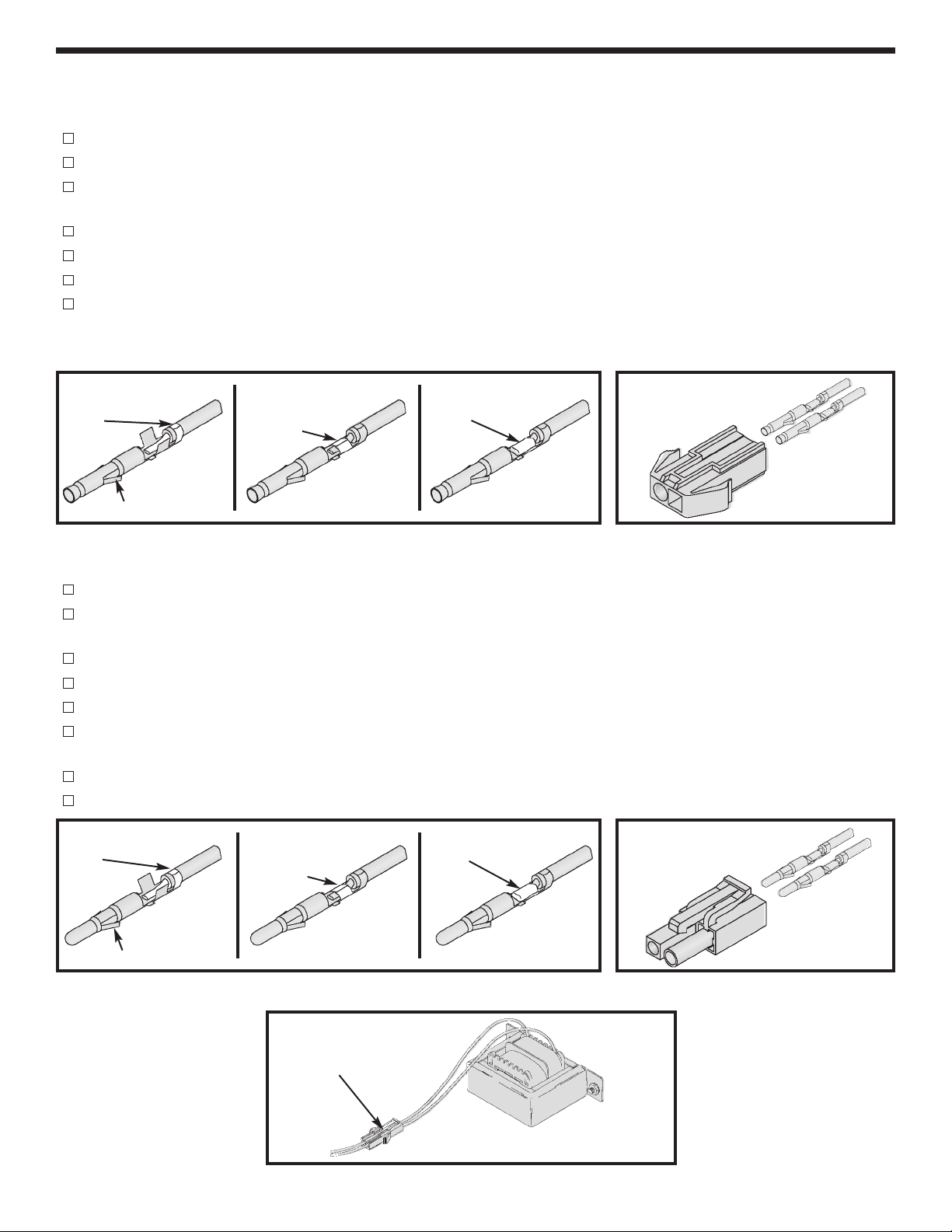
HOW TO INSTALL CONNECTORS ONTO TRANSFORMER WIRES
connector will be placed onto the primary wires of the transformer. This will allow you to remove the top panel
A
from the trainer. Follow the procedures below.
Cut a six inch length off of each black primary wire.
Strip the insulation off of each end of the six inch wires to expose 1/4” of bare wire.
Place one wire onto the female pin and crimp the outer crimp tabs with pliers over the insulation as shown
in Figure 1A.
Crimp the inner tabs with pliers onto the bare wire as shown in Figure 1B.
Solder the wire to the pin as shown in Figure 1C.
Connect the other female pin to the other wire using the same procedures above.
Insert the two pin/wire assemblies into the female housing as shown in Figure 2. Pull on the wire to check
that the pin is inserted all the way in. It should not pull out of the housing. The locking tabs should be bent
outward to hold the pin in the housing.
Female Pin
Crimp Tab
Locking Tab
Inner
Crimp Tab
SolderOuter
AB
C
Female Housing
Figure 1 Figure 2
Transformer Wires
Strip the insulation off of each of the black primary wires to expose 1/4” of bare wire.
Place the wire onto the male pin and crimp the outer crimp tabs with pliers over the insulation as shown in
Figure 3A.
Crimp the inner tabs with pliers onto the bare wire as shown in Figure 3B.
Solder the wire to the pin as shown in Figure 3C.
Connect the other male pin to the other primary wire using the same procedures above.
Insert the two pin/wire assemblies into the male housing as shown in Figure 4. Pull on the wire to check that
the pin is inserted all the way in. It should not pull out of the housing.
Connect the male and female housing as shown in Figure 5. Note that the connector only fits together one way
To detach the connector, push down on the end of the lock arm and pull the two apart.
Male Pin
Crimp Tab
Inner
Crimp Tab
SolderOuter
Male Housing
.
Locking Tab
ABC
Figure 3 Figure 4
Lock Arm
Figure 5
-12-
Page 14
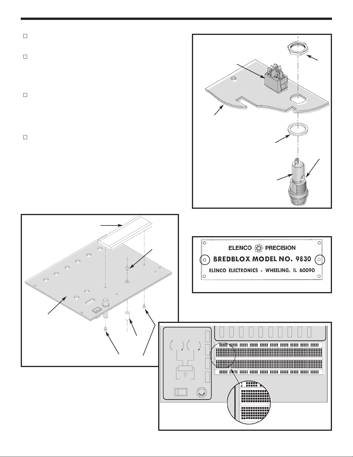
MOUNT COMPONENTS TO PANEL
Push the illuminated switch into the hole in the top
panel with the lugs as shown in Figure Q.
Install the fuse holder with the side lug in the position
shown in Figure Q. Fasten the fuse holder in place
with the nut as shown in Figure Q. Unscrew the cap
and insert the fuse into the holder.
There is a raised area on the back side of the top
panel. Screw the spacer to the raised area by
inserting a 4-40 x 1/4” flat head screw into the hole in
the raised area from the top side of the panel (see
Figure R).
When mounting the bredboard, use the holes shown in
Figure S. Mount the bredboard with two #4 x 1/4” AB
black screws from the back side of the top panel as
shown in Figure R. The negative (blue) stripe should
be on top and the numbers reading from left to right
should start with number 1 (see Figure T). CAUTION:
Do not remove the paper backing from the back of
the bredboards. Do not over-tighten the black
screws.
Back Side - Lower
Right Corner
Illuminated Switch
Top Panel
Plastic Washer
Fuse Holder
Figure Q
Nut
Side Lug
Top Panel
Figure R
Bredboard
Spacer
#4 x 1/4” AB Screws
4-40 x 1/4”
Flat Head
Screw
ON
Figure T
REGULATED
POWER SUPPLY
0
2
+
D
V
15VAC
C
30VAC
–
15VAC
OFF
V
D
0
2
Figure S
C
GND
–12
+12
+5
5
1
j
i
h
g
f
e
d
c
b
a
10
-13-
Page 15
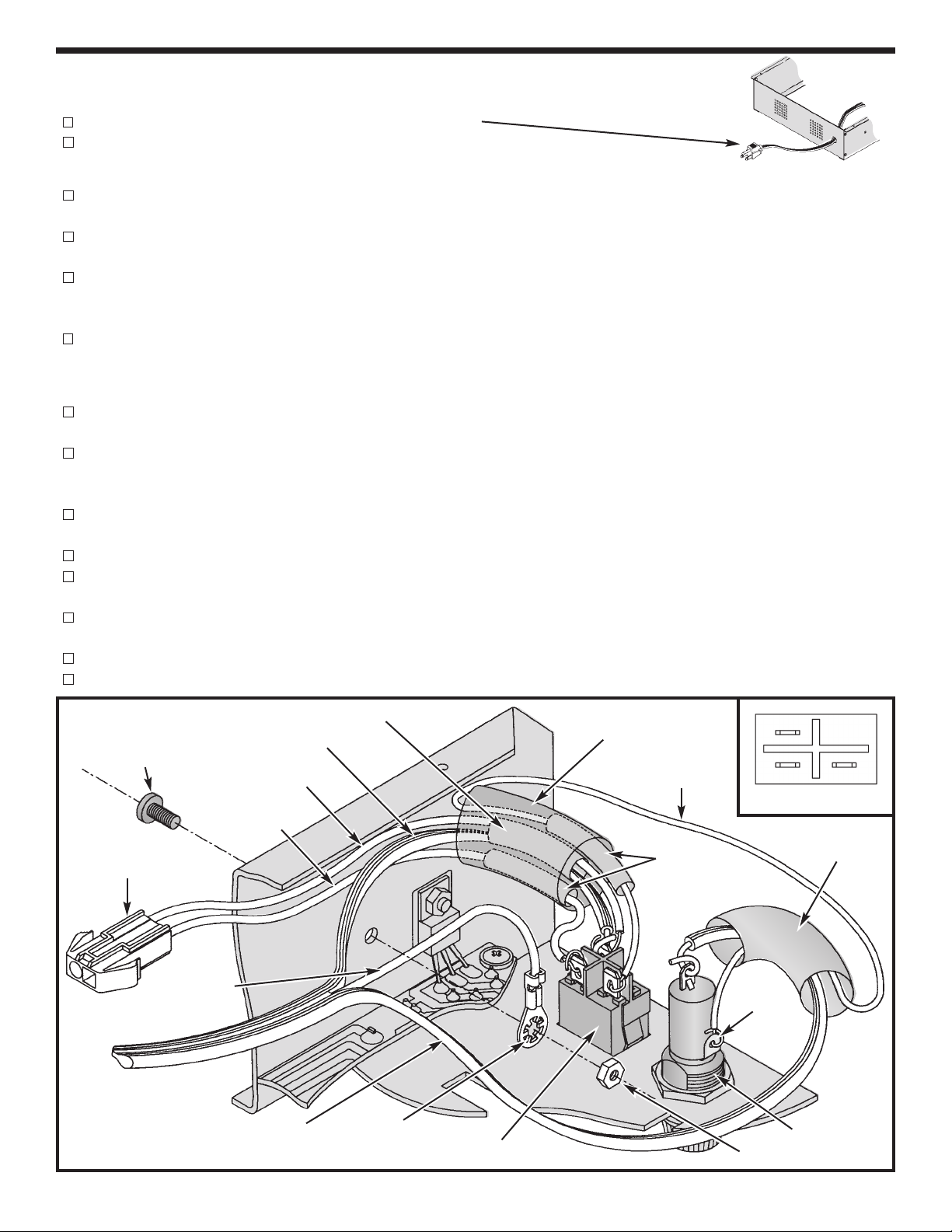
WIRE SWITCH AND FUSE HOLDER (see Figure U)
Line Cord
Slide the line cord through the back panel as shown.
Spread the three line cord wires apart 6” from the end.
Fuse
Strip the insulation off of both ends of the 6” red wire to expose 1/4” of bare wire. Pass the wire through the
1/2” diameter shrink tubing. Attach one end to the side lug on the fuse holder and then solder into place.
Pass the smooth edged line cord wire through the 1/2” diameter shrink tubing and attach to the end lug on
the fuse holder, solder into place.
Slide the shrink tubing over the fuse holder covering both lugs. Shrink the tubing for a snug fit. You may use
a hair dryer, heat gun (at lowest setting or you will melt the tubing) or the heat emitting from your soldering
iron (do not touch the tubing or the wires with the iron).
Mount the solder lug to the side panel using a 6-32 x 5/16” screw and 6-32 nut.
Switch
Disconnect the connector for the transformer.
Pass the 6” strip of red wire (leading from the side lug of the fuse holder), the (A) and (B) black transformer
wire, and the ribbed line cord wire through the 3/4” diameter piece of shrink tubing.
Cut the 2” section of 3/16” diameter shrink tubing in half to create two 1” sections. Slide a 3/16” diameter
piece of shrink tubing over the loose end of the red wire. Attach the red wire to lug 1 on the switch and
then solder into place.
Pass the black transformer wire labeled (B) through a 3/16” diameter piece of shrink tubing. Attach the wire
to lug 2 on the switch and then solder into place.
Slide the shrink tubing over lug 1 and lug 2 on the switch. Shrink the tubing into place.
Strip the insulation off of the black transformer wire (A) and the ribbed edged line cord wire to expose 1/2” of
bare wire. Twist the two bare wires together. Pass the wires through the 1/4” diameter piece of shrink tubing.
Attach the wires to lug 3 on the switch and solder into place. Slide the tubing over the lug. Shrink the tubing
into place.
Slide the 3/4” diameter shrink tubing over the switch and shrink into place.
Reconnect the connector for the transformer.
6-32 x 5/16”
Screw
Female Connector
Green Line
Cord Wire
Figure U
1/4” Dia. Shrink Tubing
Ribbed Line Cord Wire
(A) Black
Transformer Wire
(B) Black
Transformer Wire
Smooth Line
Cord Wire
Solder Lug
Switch
3/4” Dia. Shrink Tubing
6” Red Wire
3/16” Dia.
Shrink Tubing
3
2
Switch Pin-out
Shrink Tubing
Side Lug
6-32 Nut
1
1/2” Dia.
Fuse Holder
-14-
Page 16
RESISTANCE ANALYSIS OF POWER SUPPLY
Static testing of the power supply circuits. Do not plug the power supply into the 120VAC power supply
source until all resistance readings check out. The values given below are approximate.
See Figure V for locations of testing points.
Resistance
From To Circuit Ohms Measured
1 Right Side Panel Earth Ground less than 1Ω
23 On/Off Switch, Fuse Infinite (SW1 Off)
23 On/Off, Fuse 7Ω (SW1 On)
45 12V Secondary 1.5Ω
67 5V Secondary 1.2Ω
89 Variable Voltage 1.6Ω
10 GND 5-pin connector +12V Regulator Input greater than 20kΩ
11
(com)
GND (VΩ)
12 GND (B1) +5V Regulator Input greater than 20kΩ
13 GND (B1) +Variable Regulator Input greater than 20kΩ
14 (com)
25
(com)
GND (VΩ)
GND (VΩ)
26 GND (VΩ)
27 GND (5-pin connector) +5V Regulator GND less than 1Ω
28 GND (5-pin connector) +12V Regulator GND less than 1Ω
29 GND (5-pin connector) –12V Regulator GND less than 1Ω
10 15 +12V Regulator Input less than 1Ω
11 16 –12V Regulator Input less than 1Ω
12 17 +5V Regulator Input less than 1Ω
13 18 +Variable Regulator Input less than 1Ω
14 19 –Variable Regulator Input less than 1Ω
20 GND (5-pin connector) +Variable Regulator Output CCW 100Ω CW 2.12k
20 +20 (5-pin connector) +Variable Regulator Output less than 1Ω
21 GND (5-pin connector) –Variable Regulator Output CCW 100Ω CW 2.12k
21 –20 (5-pin connector) –Variable Regulator Output less than 1Ω
22 GND (5-pin connector) +5V Regulator Output greater than 5kΩ
22 B4 +5V Regulator Output less than 1Ω
23 GND (5-pin connector) +12V Regulator Output greater than 5kΩ
23 B3 +12V Regulator Output less than 1Ω
24 GND (5-pin connector) –12V Regulator Output greater than 5kΩ
24 B2 –12V Regulator Output less than 1Ω
5
4
15VAC (5-pin connector right)
15VAC (5-pin connector left)
(5-pin connector)
(5-pin connector)
(5-pin connector)
(5-pin connector)
–12V Regulator Input greater than 20kΩ
–Variable Regulator Input greater than 20kΩ
Voltage ADJ +20V Regulator
CCW <1Ω CW >1.4kΩ
Voltage ADJ -20V Regulator greater than 1.4kΩ
15VAC less than 1Ω
15VAC less than 1Ω
+30% Note: meter lead polarity CCW - Counter Clockwise CW - Clockwise VR1 & VR2 Adjustment
20A
2A COM VΩ
VΩ
COM
-15-
Page 17

Locations for Testing Points
Plug of line cord
LM-7812 LM-7912
23
28
15
•••
24
16
•••
1
29
3
2
On test points 4 - 14
use the leads of the
diodes.
5
6
8
7
9
4
10
12
11
13
14
Ground
•••
27
17
22
•••
25
20
LM-7805 LM-317
18
Figure V
–20V
+20V
B1
Pot
5-pin connector right
5-pin connector –20
GND
5-pin connector +20
5-pin connector left
Pot
•••
26
21
19
LM-337
-16-
Page 18

VOLTAGE ANALYSIS OF POWER SUPPLY
roceed with the voltage analysis only if the resistance readings were satisfactory.
P
Place the top panel on the unit. If any capacitors are inserted backwards, the panel will shield you if
they explode. Make sure that the ON/OFF switch is in the OFF position. Plug the line cord into the 120VAC
power source. Turn the unit on and let it sit for a few minutes. Turn OFF the ON/OFF switch and remove the
top panel, placing it along the left side of the trainer. Turn ON the ON/OFF switch and measure the voltage point
as listed in the chart below. The values given are approximate.
See Figure O for locations of the testing points.
From To Circuit Volts Volts Measured
15 GND +12V Regulator Input +21V
B3 GND +12V Regulator Output +12V
16 GND –12V Regulator Input –21V
B2 GND –12V Regulator Output –12V
17 GND +5V Regulator Input +12.5V
B4 GND +5V Regulator Output +5V
18 GND +20V Regulator Input +28V
25 GND Voltage ADJ +20V Regulator CCW 0V CW +18V
+20
5-pin connector
GND +20V Output
19 GND –20 Regulator Input –28V
26 GND Voltage ADJ -20V Regulator CCW 0V CW –18V
–20
5-pin connector
GND –20V Output CCW –1.25V CW –20V
15VAC 15VAC 30VAC 30VAC
5-pin 5-pin
connector connector
left right
CCW +1.25V CW +20V
+30% CCW - Counter-Clockwise CW - Clockwise
Turn unit off.
Place the top panel on top of the unit.
FUSE REPLACEMENT
1. Turn the trainer off and unplug it from 120VAC power source.
2. Unscrew fuse holder cap and remove fuse.
3. Use only a 1.25A fuse. Larger fuses or other fuse bypass will void the
warranty of the trainer.
4. Place the new fuse into the fuse holder cap and screw it back into the holder.
5. Plug trainer into 120VAC power source and turn the unit on.
-17-
Page 19

POWER SUPPLY TESTING
lug the trainer into a 120VAC outlet and switch to the “ON” position (the power switch should light). With a
P
digital voltmeter, measure the voltage outputs at the power blocks. The +12V should measure between 11.4
and 12.6 volts. The 5V supply should read between 4.75 and 5.25 volts. The –12V supply should read between
–11.4 and 12.6 volts.
Do not short the 15VAC output to ground.
Short the +12V, –12V and +5V supply to ground. They should turn off and recover when the short is removed.
If you have a 25Ω 10 watt resistor, place it across the output terminal (2 watt resistor will work, but use it only
for a few seconds). The output of the 12V supply should not change more than 0.20 volts. Do the same on the
5V supply using a 10Ω 5 watt resistor. Again, the output should not change more than 0.20 volts. In making
this test, the voltmeterleads should be clipped to the terminal directly and no to the load leads. This is to prevent
errors due to voltage drop from contact resistance of the load.
Check the variable voltage supplies in the same manner. Set the output voltage between 10-15 volts. Place
the 25Ω 10 watt resistor across the output terminal. The voltage should stay within 0.20 volts of the no load
voltage.
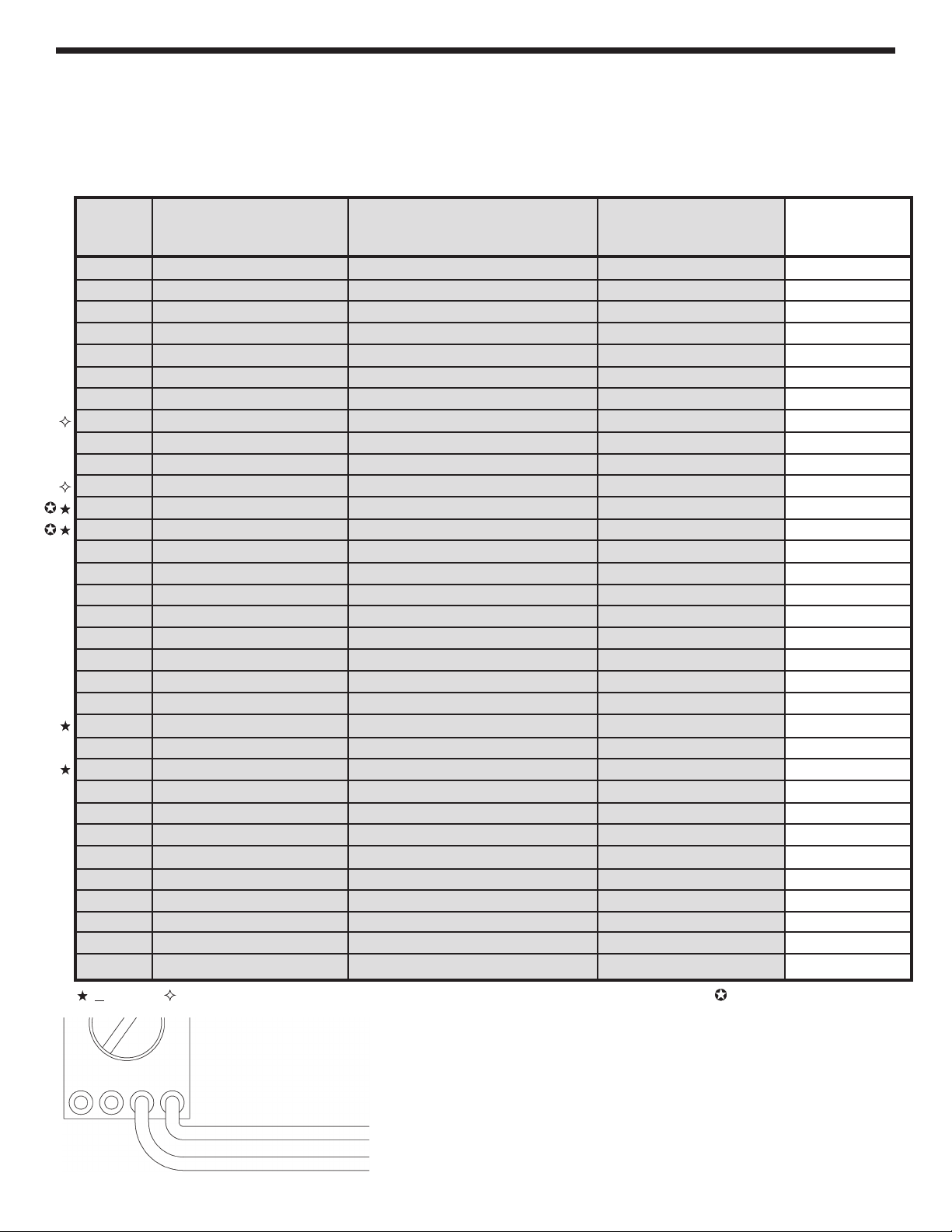
TROUBLESHOOTING CHART
This chart lists the condition and possible causes of several malfunctions. If a particular part is mentioned as
a possible cause, check that part to see if it was installed correctly. Also, check it and the parts connected to it
for good solder connections. Note: The values given in this troubleshooting chart are an approximation.
PROBLEM POSSIBLE CAUSE
Switch doesn’t light. 1. Check fuse and line cord.
Fuse blows when the unit is turned on. 1. Voltage supply shorted to GND. Use resistance analysis
chart to find short.
No or low voltage at positive variable 1. Measure for an AC voltage of 18VAC at anode of D7 & D9.
output. A. Transformer and/or secondary connection to PC
board defective
2. Measure for a DC voltage of 28VDC at pin 3 of U1 LM317.
A. Diodes D7, D9 in backwards or defective, check
capacitor C1.
3. Set the voltage for minimum 1.25VDC and measure pin 2
of U1.
A. Voltage adjusts only from 7.8 - 9.8V R1 open or
defective.
B. Voltage 27V, check VR1 connections.
No or low voltage at positive variable 1. Check that capacitor C1 1000µF is inserted in the correct
output with load. polarity.
2. Check ripple on pin 3 of U1. 8VP-P Max.
A. Capacitor C1, and/or diodes D7, D9 defective.
-18-
Page 20

PROBLEM POSSIBLE CAUSE
No voltage at negative variable output. 1. Measure for an AC voltage of 18VAC at cathode of D8, D10.
A. Transformer and/or secondary connection to PC board
defective.
2. Measure DC voltage of –28VDC at pin 2 of U5 LM337.
Set voltage for minimum –1.25VDC and measure pin 3 of U5.
3.
A. Voltage adjusts only from –7.8 to –9.8V R2 open or
defective.
B. Voltage –27V, check VR2 connections.
No or low voltage at negative variable 1. Check to see if capacitor C5 1000µF is inserted in the
output with load. correct polarity.
2. Check ripple on pin 2 of U5. 6VP-P max.
A. Capacitor C5 and/or diodes D8, D10 defective.
No +12V at output. 1. Measure an AC voltage of 15VAC at anode of D1, D3.
A. Transformer and/or secondary connection to PC board
defective.
2. Measure for a DC voltage of 21VDC at pin 1 of U2 LM7812.
A. Diodes D1, D3 in backwards or defective, check
capacitor C1.
3. Measure for a DC voltage of 12VDC on pin 3 of U2.
A. U2 LM7812 defective or open ground.
No +12V at output with load. 1. Check capacitor C2 1000µF is inserted in the correct
polarity.
2. Check ripple on pin 1 of U2. 7VP-P Max.
A. Capacitor C2 or diodes D1, D3 defective.
No –12V at output. 1. Measure an AC voltage of 15VAC at anode of D2, D4.
A.Transformer and/or secondary connection to PC board
defective.
2. Measure for a DC voltage of -21VDC at pin 2 of U4 LM7912.
A. Diodes D2, D4 in backwards or defective, check
capacitor C4.
3. Measure for a –12VDC voltage on pin 3 of U4.
A. U4 LM7912 defective or open ground.
No –12V at output with load. 1. Check capacitor C4 is inserted in the correct polarity.
2. Check ripple on pin 2 of U3. 7VP-P Max.
A. Capacitor C4 and/or diodes D1, D3 defective.
No +5VDC at output 1. Measure an AC voltage of 9VAC at anode of D5, D6.
A. Transformer and/or secondary connection to PC board
defective.
2. Measure for a DC voltage of 12VDC at pin 1 of U3 LM7805.
A. Diodes D5, D6 in backwards or defective, check
capacitor C3.
3. Measure for a 5VDC voltage on pin 3 of U3 LM7805.
A. U3 LM7805 defective or open ground.
No +5VDC at output with load. 1. Check that capacitor C3 is inserted in the correct polarity.
2. Check ripple on pin 1 of U3. 4VP-P Max.
A. Capacitor C3 and/or diodes D5, D6 defective.
-19-
Page 21

FINAL ASSEMBLY
If you are immediately going to build the remaining sections, do not continue with the instructions on
this page and proceed to page 22.
Fasten the front panel in
place with four #6 x 3/8”
thread cutting screws, as
shown in Figure W.
Knobs
Nuts 7mm
Fasten the PC board to the
spacer on the front panel
with a fiber washer and a
4-40 x 1/4” screw (from
Power Supply Section)
from the foil side of the PC
board, in the location
shown in Figure X.
Fasten the pots to the front
panel with an 8mm washer
and a 7mm nut, as shown
in Figure W.
Turn the shafts on the two
switches fully counterclockwise. Push the knobs
onto the shafts so that the
line on the knob is in line with
the end of the circle on the
front panel (see Figure Y). If
the knob is loose on the
shaft, insert a screwdriver
into the slot and expand the
slot slightly (see Figure Z).
Washers 8mm
Nuts 7mm
Washers 8mm
#6 x 3/8” Thread
Cutting Screws
#6 x 3/8” Thread
Cutting Screws
Figure W
4-40 x 1/4” Screw
Figure X
Fiber Washer
-20-
FigureY
Figure Z
Page 22

INSTALL COMPLETED UNIT INTO CASE
Latch the case lid down. Remove the protective backing from the case label. Stick the label in the depression
in the middle of the case lid.
Tie a knot in the line cord 12” from the switch. See Figure AA for the location of the line cord hole in the case.
Insert the line cord into the hole through the slot. To open up the slot, press down on one side of the slot
(see Figure BB). Insert the bushing into the hole and pull on the line cord until the knot is snug against the
bushing.
O
Insert the unit into the case at a 45
screws in the corner holes of the panel.
The line can be neatly stored in the bin shown in Figure AA. Gather up the line cord and insert it into the bin.
Insert the line cord fastener into the slots to the hole in place, as shown in Figure CC.
angle, bottom edge first. Secure into place with four 6 x 3/8” chrome
Figure AA
Figure BB
Figure CC
-21-
Page 23

CIRCUIT DESCRIPTION
he power supply features two variable output voltages and three fixed 12V, –12V and 5V variable output voltages
T
are 1.25V to 20V and –1.25 to –20V at up to 1 ampere maximum current. All supplies are regulated to better than
0.2V when going from no load to full load. Varying the input AC voltage from 105 to 135V will have practically no effect
on the output voltages. This is because of the specially designed ICs used in the XK-700 Digital/Analog Trainer.
Severe overloading or even shorting the output circuits will not damage the supplies. Special turn-off circuits in the
ICs sense the overload and turn off the output.
THE POSITIVE 1.25 TO 20V POWER SUPPLY
Figure 1 shows a simplified circuit diagram of the positive supply. It consists of a power transformer, a DC
rectifier stage and the regulator stage.
120VAC
Input
Transformer
120V to 17V
TRANSFORMER
The transformer T1 serves two purposes. First, it reduces the 120VAC input
to 17VAC to allow the proper voltage to enter the rectifier stages. Second,
it isolates the power supply output from the 120VAC line. This prevents the
user from dangerous voltages should he or she be standing in a grounded
area.
ACTO DC CONVERTER
The AC to DC converter consists of diodes D1, D3 and capacitor C1.
Transformer T1 has two secondary windings which are 180 degrees out of
phase. The output at each winding is shown in Figure 2A and 2B.
Diodes are semiconductor devices that allow current to flow in only one
direction. The arrow in Figure 3 points to the direction that the current will
flow. Only when the transformer voltage is positive will current flow through
the diodes. Figure 3 shows the simplest possible rectifier circuit. This circuit
is known as a half-wave rectifier. Here the diode conducts only half of the
time when the AC wave is positive as shown in Figure 2C. Use of this circuit
is simple but inefficient. The big gap between cycles require much more
filtering to obtain a smooth DC voltage.
17VAC 20VDC 1.25 - 15V
Simplified diagram of positive power supply
AC to DC
Converter
Voltage
Regulator
Regulated
Figure 1
Voltage Waveform for Supply
F) Output of capacitor C1
Ripple depends on load
current (expanded).
Figure 2
Output
A) Transformer
Winding AB
B) Transformer
Winding BC
C) Output of
diode D1.
D) Output of
diode D2.
E) Total of diodes
D1 & D2.
20V
By the addition of a second diode and transformer winding we can fill in the
gap between cycles as shown in Figure 4. This circuit is called full-wave
rectification. Each diode conducts when the voltage is positive. By adding the
two outputs, the voltage presented to capacitor C1 is more complete, thus
easier to filter, as shown in Figure 2E. When used in 60 cycles AC input
power, the output of a full wave rectifier will be 120 cycles.
Capacitor C1 is used to store the current charges, thus smoothing the DC
voltage. The larger the capacitor, the more current is stored. In this design,
1000µF capacitors are used, which allows about 5 volts AC ripple when one
amp is drawn.
-22-
Half Wave Rectifier
Figure 3
Full Wave Rectifier
Figure 4
Page 24

n practice, the current through the diodes is not as shown in Figure 2C.
I
Because capacitor C1 has a charge after the first cycle, the diode will not
conduct until the positive AC voltage exceeds the positive charge in the
capacitor. Figure 5 shows a better picture of what the current flow looks
like assuming no loss in the diode. It takes a few cycles for the voltage to
build up on the capacitor. This depends on the resistance of the winding
and the diode. After the initial start-up, there will be a charge and
discharge on the capacitor depending on the current drawn by the output
load. Remember, current only flows through the diode when the anode is
more positive than the cathode. Thus, current will flow in short bursts as
A) Transformer
Winding
B) Voltage C1
C) Current
through diodes
Figure 5
0V
2
Peak
20V
shown in Figure 5.
The DC load current may be one ampere, but the peak diode current may be three times that. Therefore, the
diode rating must be sufficient to handle the peak current. The 1N4001 has a peak current rating of 10 amps.
REGULATOR CIRCUIT
The regulator circuit in the power supply consists of a LM-317 integrated circuit.
This IC is specially designed to perform the regulation function. Figure 6 shows
a simplified circuit of how the LM-317 IC works.
Current
ource
S
Equalized
to 1 Meg.
Q2
Q3
Q5
4
Q
2V
Output
R1
Transistors Q1 and Q2 form a circuit known as a differential amplifier. The base
1.5V
Q1
R2
of transistor Q1 is connected to a stable 1.5V reference voltage. The base of
Q2 is connected to the regulator output circuit through a voltage divider
Divider
network. The collector of transistor Q2 is connected to a current source. This
basically is a PNP transistor biased to draw about 1mA of current. Transistor
Q2 sees the current source as a very high resistor of about 1 meg ohms. Thus,
Figure 6
the gain of transistor Q2 is extremely high.
Transistor Q5 is called the pass transistor. It controls the current reaching the output. Transistor Q3 and Q4 are
emitter followers. Their function is to raise the impedance of the pass transistor. Note that transistors Q2, Q3,
Q4, Q5 and resistor R1 form a closed loop. Also, note that the feedback to the base of Q2 is negative, that is,
when the base of Q2 goes positive, the output at emitter Q5 goes negative. Now if the 2 volt output voltage
goes down because of current drain at the output, the base of Q2 will drop, forcing the collector voltage to go
higher. This will bring the output voltage back to 2 volts. This is the basis of all negative feedback regulators.
Another feature of the LM-317 regulator if to protect the IC against overload and output shorts. If the IC is
overloaded, the junction of an overload transistor will overheat. A transistor will sense this overheating and shut
down transistor Q5.
The LM-317 IC is basically a 1.25 volt regulator. To be able to vary the output
from 1.25V to 20V, we stack the IC on the a DC voltage as shown in Figure 7.
When VR1 equals 0, the output voltage is 1.25 volts as determined by the LM317 IC. Note that the voltage across VR1 will equal the 1.25 volts across R1,
therefore the output voltage will be 2.5 volts. When VR1 is 5 times R1, the
LM-317
1.25 - 15V
R1
VR1
output voltage is 6.25 volts. As you can see, varying resistor VR1 will vary the
voltage from 1.25 volts to 20 volts.
THE NEGATIVE VOLTAGE REGULATOR
Figure 7
The theory of the negative regulator is the same as the previously discussed positive regulator. The basic
difference is that diodes D1 and D3 are reversed, producing a negative voltage across capacitor C1. The LM317 IC is designed to operate from a negative supply.
-23-
Page 25

SCHEMATIC DIAGRAM - POWER SUPPLY SECTION
REV-F
22
20
26
25
18
19 21
10
11
27
17
2200µF
25V
23
28
15
12
24
29
16
14
13
8
4
6
7
5
9
Test Point
#
3
1
2
-24-
Page 26

QUIZ - POWER SUPPLY SECTION
INSTRUCTIONS - Complete the following examination and check your answers carefully.
. AC voltage is supplied to the rectifier stages by the . . .
1
A. step-up transformer.
B. step-down transformer.
C. 1 to 1 transformer.
D. AC to DC transformer.
2. The secondary windings of the transformer are . . .
3. Diodes allow current to flow . . .
4. What circuit is more efficient for rectifying AC to DC?
5. The DC voltage is smoothed by using a . . .
6. An inefficient rectification circuit usually contains . . .
7. The maximum current that a diode can handle is determined by . . .
8. The LM-317 will shut down when . . .
9. The LM-317 regulator contains . . .
10. The LM-317 is basically . . .
O
A. 90
out of phase.
B. 180Oout of phase.
O
C. 270
out of phase.
D. 320Oout of phase.
A. when the anode is more negative than the cathode.
B. when the cathode is more positive than the anode.
C. in one direction.
D. when a negative or positive voltage is on the anode.
A. Hartley oscillator.
B. Half-walf.
C. Schmitt trigger.
D. Full wave.
A. half-wave rectification circuit.
B. small value capacitor with a high voltage value.
C. Large value capacitor.
O
D. 90
out of phase.
A. large gaps between cycles.
B. twice the AC voltage needed.
C. more diodes.
D. all of the above.
A. the transformer’s current rating.
B. the amount of AC ripple.
C. three times the diode rating.
D. peak current rating.
A. the output voltage is too high.
B. no current is being drawn.
C. the junction overheats.
D. the output voltage drops to 1.25V.
A. a pass transistor.
B. a constant current source.
C. a differential amplifier.
D. all of the above.
A. a 1.25V regulator.
B. a 6.25V regulator.
C. a 2.5V regulator.
D. a negative voltage regulator.
Answers: 1. B; 2. B; 3. C; 4. D; 5. C; 6. D; 7. D; 8. C; 9. D; 10. A
-25-
Page 27

AN-550-C
XK-550 ANALOG KIT (AN-700-C) PARTS LIST
RESISTORS
Qty. Symbol Value Color Code Part #
2 R14, R44 100Ω 5% 1/4W brown-black-brown-gold 131000
1 R5 200Ω 5% 1/4W red-black-brown-gold 132000
2 R46, R47 330Ω 5% 1/4W orange-orange-brown-gold 133300
1 R12 1kΩ 5% 1/4W brown-black-red-gold 141000
1 R49 2kΩ 5% 1/4W red-black-red-gold 142000
2 R7, R11 4.7kΩ 5% 1/4W yellow-violet-red-gold 144700
1 R3 6.8kΩ 5% 1/4W blue-gray-red-gold 146800
1 R13 8.2kΩ 5% 1/4W gray-red-red-gold 148200
1 R10 10kΩ 5% 1/4W brown-black-orange-gold 151000
1 R6 12kΩ 5% 1/4W brown-red-orange-gold 151200
3 R4, R45, R48 22kΩ 5% 1/4W red-red-orange-gold 152200
1 R9 47kΩ 5% 1/4W yellow-violet-orange-gold 154700
1 R8 51kΩ 5% 1/4W green-brown-orange-gold 155100
1 VR8 100kΩ Trim Pot 191610
1 VR5 10kΩ Pot 192531
2 VR6, VR7 100kΩ Pot 192612
CAPACITORS
Qty. Symbol Value Description Part #
1 C27 5pF (5) Discap 205010
1 C26 22pF (22) Discap 212210
1 C23 100pF (101) Discap 221017
1 C18 .001µF (102) Mylar 231017
1 C25 .0022µF (222) Discap 232216
1 C19 .01µF (103) Mylar 241017
1 C20 .1µF (104) Mylar 251017
1 C21 1µF 50V Electrolytic 261047
2 C22, C24 10µF 25V Electrolytic 271045
SEMICONDUCTORS
Qty. Symbol Value Description Part #
2 D16, D17 1N4148 Diode 314148
2 Q1, Q3 2N3904 Transistor PNP 323904
1 Q2 2N3906 Transistor NPN 323906
1 U10 LF357 Integrated Circuit 330357
1 U6 XR2206 Integrated Circuit 332206
MISCELLANEOUS
Qty. Symbol Description Part #
1 SW2 Switch Rotary 12-pin 542206
1 SW3 Switch Rotary 16-pin 542405
5 Knob Push-on 622009
3 Nut 7mm 644101
2 Nut 9mm 644102
3 Washer Flat 8mm 645101
2 Washer Flat 9mm 645103
1 U10 IC Socket 8-Pin 664008
1 U6 IC Socket 16-Pin 664016
2 B5, B6 4-Pin Bredblox 665204
1 Solder 9ST4A
-26-
Page 28

INTRODUCTION - ANALOG SECTION
The Analog Section of your trainer contains a complete function generator capable of producing sine, square,
and triangle waveforms. The frequency of this generator can be continuously varied from 1 hertz to over
100,000 hertz in five steps: 10, 100, 1k, 10k, and 100k. A fine frequency control makes selection of any
frequency in between easy. The amplitude of the waveforms are adjustable from 0-15Vpp. A waveform of
function generator capable of producing sine, square and triangle waveform outputs has a wide range of
applications in electrical measurements and laboratory instrumentation. This complete function generator
system is suitable for experimentation and applications by the student. The entire function generator is
comprised of a single XR-2206 monolithic IC and a limited number of passive circuit components.
SPECIFICATIONS
Waveforms - Sine, square, triangle and complementary square.
Frequency - 1Hz to 100kHz in 5 steps continuously variable.
Fine frequency adjust - 10:1 approximate.
Amplitude variable 0-15 Vpp.
Output impedance 330 ohms: short protected.
DC offset change 10V from zero crossing.
1
6
7
2 3 4 5
USERS DESCRIPTION OF FRONT PANEL CONTROLS
1. WAVEFORM - Selects square, triangle or sine waveform at the FREQ output.
2. COURSE FREQUENCY - Selects five ranges of frequencies 10, 100, 1k, 10k and 100k hertz.
3. FINE FREQUENCY - Allows easy selection of desired frequency according to the frequency range.
4. AMPLITUDE - Controls the amplitude of the FREQ output signal from 0-15Vpp.
5. DC OFFSET - Controls the DC level of the FREQ output signal. The DC level may be varied 10 volts from
zero level.
6. CLK - A 4-pin output block for function generator’s square wave. The amplitude of the signal is 5Vpp and
frequency is dependent on WAVEFORM selection.
7. FREQ - A 4-pin output block for function generator’s signals, output is dependent on WAVEFORM selection
and frequency is set by COURSE FREQ control. The amplitude of the output is variable from 0-15Vpp.
-27-
Page 29

INSTALL COMPONENTS TO PC BOARD
Start Here
J9 - Jumper Wire
(see Figure A)
C25 - .0022µF (222) Discap
J10 - Jumper Wire
J25 - Jumper Wire
(see Figure A)
VR8 - 100kΩ Trim Pot
(see Figure E)
C26 - 22pF (22) Discap
C23 - 100pF (101) Discap
J11 - Jumper Wire
J12 - Jumper Wire
J13 - Jumper Wire
(see Figure A)
U10 - IC socket 8-pin
U10 - LF357 IC
(see Figure B)
R8 - 51kΩ 5% 1/4W Resistor
(green-brown-orange-gold)
R11 -
4.7kΩ
5%
1/4W Resistor
(yellow-violet-red-gold)
C27 - 5pF (5) Discap
Continue
R5 - 200Ω 5% 1/4W Resistor
(red-black-brown-gold)
J8 - Jumper Wire
(see Figure A)
R3 - 6.8kΩ 5% 1/4W Resistor
(blue-gray-red-gold)
R4 - 22kΩ 5% 1/4W Resistor
(red-red-orange-gold)
U6 - IC socket 16-pin
U6 - XR2206 IC
(see Figure B)
R49 - 2kΩ 5% 1/4W Resistor
(red-black-red-gold)
Q3 - 2N3904 Transistor
(see Figure C)
R10 - 10kΩ 5% 1/4W Resistor
(brown-black-orange-gold)
C24 - 10µF 25V Lytic
(see Figure D)
R7 - 4.7kΩ 5% 1/4W Resistor
(yellow-violet-red-gold)
R9 - 47kΩ 5% 1/4W Resistor
(yellow-violet-orange-gold)
Figure A
Cut a piece of bare wire long
enough so that 1/4” of wire
passes through each hole in
the PC board after the wire is
formed (provided in the
second package).
Figure B
IC
Notch
Socket
Insert the IC socket into the PC
board with the notch in the
direction shown on the top
legend. Solder the IC socket
into place. Insert the IC into the
socket with the notch in the
same direction as the notch on
the socket.
-28-
Figure C
Flat
Mount the
transistor with
the flat side in
the direction
shown on the
top legend.
Figure D
Electrolytics have a polarity
marking on them indicating the
negative (–) lead. The PC board
is marked to show the lead
positions.
Mount the
capacitors
horizontal to the PC
board. Bend the
leads at right
angles and then
insert the leads into
the PC board.
Polarity
Mark
(–)
(+)
Page 30

INSTALL COMPONENTS TO PC BOARD
Start Here
B6 - 4-pin Bredblox
(see Figure F)
D16 - 1N4148 Diode
(see Figure G)
R14 - 100Ω 5% 1/4W Resistor
(brown-black-brown-gold)
B5 - 4-pin Bredblox
(see Figure F)
R12 - 1kΩ 5% 1/4W Resistor
(brown-black-red-gold)
R44 - 100Ω 5% 1/4W Resistor
(brown-black-brown-gold)
D17 - 1N4148 Diode
see Figure G)
(
J23 - Jumper Wire
(see Figure A)
Continue
R48 - 22kΩ 5% 1/4W Resistor
(red-red-orange-gold)
Q1 - 2N3904 Transistor
(see Figure C)
R47 -
330Ω5%1/4W Resistor
(orange-orange-brown-gold)
R46 - 330Ω 5% 1/4W Resistor
(orange-orange-brown-gold)
R45 - 22kΩ 5% 1/4W Resistor
(red-red-orange-gold)
J16 - Jumper Wire
J15 - Jumper Wire
J14 - Jumper Wire
(see Figure A)
Q2 - 2N3906 Transistor
(see Figure C)
Figure E
Mount the trim pot to the PC board as
shown below.
Figure EA
Bend the capacitors at a 45oangle before
soldering it to the PC board.
Figure F
Hold the bredblox down flush
to the PC board from the top
legend side and solder the
metal pins in place. Then,
melt the plastic pins with your
soldering iron to hold the
bredblox down as shown. Retin the solder tip afterwards.
Plastic Pins
Melt Pins
Figure G
Diodes have polarity. Mount with
band in the direction shown on the
PC board.
Band
-29-
Page 31
INSTALL COMPONENTS TO PC BOARD
Figure H
Start Here
J18 - Jumper Wire
(see Figure A)
R13 -
8.2kΩ
5%
1/4W Resistor
(gray-red-red-gold)
J17 - Jumper Wire
(see Figure A)
C18 - .001µF (102) Mylar
(see Figure EA)
R6 - 12kΩ 5% 1/4W Resistor
(brown-red-orange-gold)
Mount down flush with
PC board. The value
may be marked on the
back side of pot.
Cut off excess lead
length after soldering.
Potentiometers
Mount down flush with PC board.
Note: SW2 has 12 pins and SW3
has 16 pins.
Cut off
tab
Switches
Cut off
tab
Figure I
VR6 - 100kΩ Pot
(see Figure H)
VR5 - 10kΩ Pot
(see Figure H)
VR7 - 100kΩ Pot
(see Figure H)
SW2 - SW Rotary 12-Pin
(see Figure I)
SW3 - SW Rotary 16-Pin
(see Figure I)
Continue
C21 - 1µF 50V Electrolytic
(see Figure D)
C22 - 10µF 25V Electrolytic
(see Figure D)
C20 - .1µF (104) Mylar
(see Figure EA)
C19 - .01µF (103) Mylar
(see Figure EA)
-30-
Page 32

RESISTANCE ANALYSIS OF ANALOG SECTION
tatic testing of the analog circuits. Do not plug in the power supply into 120VAC power source until all
S
resistance readings check out. The values given below are approximated.
SET SW3 TO SQUARE WAVE (refer to top panel)
From To Circuit Ohms Resistance Measured
Pin 11 (U6) Pin 3 (U10) Square Wave VR5 CCW 12.3kΩ
Pin 11 (U6) Pin 3 (U10) Square Wave VR5 CW 6.7kΩ
SET SW3 TO TRIANGLE WAVE
From To Circuit Ohms Resistance Measured
Pin 2 (U6) Pin 3 (U10) Triangle Wave VR5 CCW 14.7kΩ
Pin 2 (U6) Pin 3 (U10) Triangle Wave VR5 CW 4.7kΩ
Pin 13 (U6) Pin 14 (U6) Triangle Wave Greater than 1kΩ
SET SW3 TO SINE WAVE
From To Circuit Ohms Resistance Measured
Pin 2 (U6) Pin 3 (U10) Sine Wave VR5 CCW 14.7kΩ
Pin 2 (U6) Pin 3 (U10) Sine Wave VR5 CW 4.7kΩ
Pin 13 (U6) Pin 14 (U6) Sine Wave 200Ω
Pin 3 (U6) GND (B1) Mult VR8 CCW < 10Ω
Pin 3 (U6) GND (B1) Mult VR8 CW 100kΩ
Pin 4 (U6) +12V (B3) VCC Less than 3Ω
Pin 7 (U6) –12V (B2) Fine Freq Adj VR7 CCW 108.2kΩ
Pin 7 (U6) –12V (B2) Fine Freq Adj VR7 CW 8.2kΩ
Pin 12 (U6) –12V (B2) GND Less than 3Ω
30% CCW - Counter-Clockwise CW - Clockwise
VR8
U10
1
2
3
4
8
7
6
5
U6
1
16
15
2
3
14
13
4
12
5
11
6
7810
9
-31-
Page 33

VOLTAGE ANALYSIS OF ANALOG SECTION
roceed with the voltage analysis only if the resistance readings were satisfactory. The values given below
P
are approximate.
The following measurements will be taken from the copper side of the PC board. Turn the unit on and place it
upside down.
See Figure J for locations of the testing points.
From To Circuit Volts Volts Measured
Pin 4 (U6) GND (B1) U6 Vcc +12V
Pin 12 (U6) GND (B1) U6 GND –12V
Pin 7 (U10) GND (B1) U10 Vcc +12V
Pin 4 (U10) GND (B1) U10 Vcc– –12V
U6
1
16
15
2
3
14
13
4
12
5
11
6
7810
9
12
4
U10
7
GND
1
8
2
7
3
6
4
5
4
Turn unit right side up. Figure J
TESTING THE FUNCTION GENERATOR
Note: Use the knobs when turning the switches.
TESTING THE SINE WAVE
1. Set your meter to the 200mV DC range.
2. Connect the red meter lead to the 4-pin breadblock marked FREQ and the black lead wire to the 4-pin
breadblock marked GND.
3. Set the WAVEFORM knob to SINE, COARSE FREQUENCY knob to 1k and the FINE ADJ and AMPLITUDE
knobs fully clockwise.
4. Set the DC offset to the middle position. Then, turn on the trainer.
-32-
Page 34

. Set VR8 fully counter-clockwise.
5
6. Adjust the DC OFFSET knob until the meter reads 0 volts DC.
7. Set the meter to the 20 volts AC range and slowly turn VR8
clockwise until the meter reads 5.8 volts AC.
Note: Adjusting the DC offset will affect the VAC readings.
TESTING THE TRIANGLE WAVEFORM
1. Switch the WAVEFORM knob to its triangle wave setting.
2. With the meter set to the 20 volts AC range, you should read about
6.3 volts AC.
TESTING THE SQUARE WAVEFORM
1. Switch the WAVEFORM knob to its square wave setting.
2. Set your meter to the 20 volts AC range, you should now read about 12.5 volts AC.
Turn the unit off and unplug it from the AC outlet.
Trim Pot Adjustment
TROUBLESHOOTING CHART
This chart lists the condition and possible causes of several malfunctions. If a particular part is mentioned as
a possible cause, check that part to see if it was installed correctly. Also, check it and the parts connected to it
for good solder connections.
PROBLEM POSSIBLE CAUSE
No wave form at FREQ 1. Check voltage at pins 4 (+12V) and 12 (–12V) of U6.
2. Check for wave forms at pin 2 of U6 and pin 3 of U10.
A. Check R3-4, R7, R13, C18-22, C24, SW2-3, VR5 & VR7.
3. Measure voltage at pins 7 (+12V) and 4 (–12V) of U10.
4. Check R8, R9, R11, R14, R44-48, D16, D17, Q1 and Q2.
No sine, triangle or low amplitude 1. Check U6 pin 2 for wave form.
A. Check VR8, voltage to IC.
Saw wave in sine position 1. R5 wrong value.
Wave forms clip top or bottom 1. Measure voltage at pins 7 (+12V) and 4 (–12V).
2. Adjust VR8.
3. Check R7, R9, R11, R14, R44-49, D16-17 and Q2-3.
No CLK wave output or low amplitude 1.Check pin 11 of U6 for square wave.
A. Check Q2 shorted to ground.
B. Check R10, R12 and Q3.
C. Defective IC.
No square wave or low amplitude 1.Check pin 11 of U6 for square wave.
(FREQ output) A. Check Q2 shorted to ground.
B. Check R3, R49, SW3.
C. Defective IC.
Outputs wrong frequency 1. Check C18-22, C24, R13, SW2 and VR7.
DC offset not working 1. Check voltage on VR6 for +12V and –12V; check R8.
-33-
Page 35

FINAL ASSEMBLY
If you are immediately going to build the remaining section, do not continue with the instructions on
this page, proceed to page 35.
Fasten the front panel in
place with four #6 x 3/8”
thread cutting screws, as
shown in Figure K.
Fasten the PC board to the
spacer on the front panel
with a fiber washer and a 440 x 1/4” screw from the foil
side of the PC board, in the
location shown in Figure L.
Fasten the pots to the front
panel with an 8mm washer
and a 7mm nut, as shown
in Figure K.
Turn the shafts on the two
switches fully counterclockwise. Push the knobs
onto the shafts so that the
line on the knob is in line
with the “Squarewave” on
the waveform control and
“10” on the Coarse
Frequency control (see
Figure M).
If the knobs are loose on
the shafts, insert a
screwdriver into the slot
and expand the slot slightly
(see Figure O).
Nuts 7mm
Washers 8mm
Figure K
Knobs
#6 x 3/8” Thread
Cutting Screws
Nuts 8mm
Washers 9mm
Nut 7mm
Washer 8mm
#6 x 3/8” Thread
Cutting Screws
Turn the shafts on the pots fully counter-clockwise. Push the knobs onto the shafts so that the line on the
knob is in line with the end of the circle on the front panel, as shown in Figure N.
If the knobs are loose on the shafts, insert a screwdriver into the slot and expand the slot slightly (see Figure O).
4-40 x 1/4” Screw
Fiber Washer
100
10
WAVE FORM COARSE FREQ
10k
100k
1k
Figure M
AMPLITUDE
Figure L
Figure N
Figure O
-34-
Page 36

CIRCUIT DESCRIPTION
he function generator frequencies are produced by an XR2206
T
integrated circuit. This IC is capable of producing high quality sine,
square and triangle waveforms of high stability and accuracy. The
output waveform can be both amplitude and frequency modulated
by an external voltage. Figure P shows the block diagram of the
XR2206 IC.
Functional Block Diagram
M Input
A
Sine/Saw
utput
O
ult. Out
M
1
+1
2
3
V+
4
ultiplier
M
S
haper
S
nd
a
ine
16
15
14
13
Symmetry
ADJ.
aveform
W
ADJ.
The XR2206 is comprised of four functions blocks, a voltage
controlled oscillator (VCO), an analog multiplier and sine shaper, a
unity gain buffer amplifier, and a set of current switches.
The VCO actually produces an output frequency proportional to an
input current. Across pins 5 and 6, a timing capacitor is switched
Timing
Capacitor
iming
T
esistor
R
5
CO
V
6
7
urrent
C
Switches
8
12
11
10
9
Ground
Sync
utput
O
Bypass
FKS
nput
I
in to give 5 different ranges of frequencies via COARSE FREQ
switch. On pin 7, the FINE FREQ ADJ variableresistor controls the
Figure P
actual frequency output. These two components form the RC time constants for the oscillator frequency.
TheVCO produces a square wave signal. This square waveis sent to a shaper and converted into a sine wave.
QUIZ - ANALOG SECTION
INSTRUCTIONS: Complete the following examination and check your answers carefully.
1. The analog multiplier is part of . . .
A. the voltage controlled oscillator.
B. unity gain buffer amplifier.
C. four function blocks.
D. timing capacitor circuit.
2. Increasing the current of the VCO will effect the . . .
A. amplitude.
B. DC offset.
C. AM modulation.
D. frequency.
3. The RC time constant is determined by . . .
A. pins 5 and 6.
B. voltage controlled oscillator.
C. pin 7 and a variable resistor.
D. components on pins 5, 6, and 7.
4. What pins on the 2206 IC are used to change the
sine wave to a saw wave?
A. 5, 6
B. 15, 16
C. 13, 14
D. 4, 12
5. Adjusting P4 from +12V to –12V effects . . .
A. sine wave amplitude.
B. modulation.
C. frequency stability.
D. DC offset.
6. Coarse frequency is set by . . .
A. P6.
B. capacitor C11 through C15.
C. C21.
D. P1 and SW9.
7. A 1 volt DC level on the FM input will . . .
A. shift the frequency 1kHz.
B. shift the frequency to DC.
C. have no effect.
D. shift the frequency 1MHz.
8. The square wave and CLK output are 180
O
out
of phase because . . .
A. Q2 inverts the CLK output.
B. Q1 inverts the square wave output.
C. a negative voltage is applied to P5.
D. pin 12 is tied to –12V.
9. Clipping of the sine wave outputs can be
corrected by . . .
A. P5.
B. the DC offset pot.
C. lowering the +5V power supply.
D. none of the above.
10. The sync output produces . . .
A. a sine wave.
B. a saw wave.
C. voltage spikes.
D. a square wave.
-35-
Answers: 1. C; 2. D; 3. D; 4. C; 5. D; 6. B; 7. C; 8. A; 9. D; 10. D
Page 37

SCHEMATIC DIAGRAM - ANALOG SECTION
-36-
Page 38
DG-550-D
XK-550 DIGITAL KIT (DG-550-D) PARTS LIST
RESISTORS
Qty. Symbol Value Color Code Part #
8 R36 - R43 120Ω 5% 1/4W brown-red-brown-gold 131200
1 R15 220Ω 5% 1/4W red-red-brown-gold 132200
4 R16 - R19 1kΩ 5% 1/4W brown-black-red-gold 141000
16 R20 - R35 100kΩ 5% 1/4W brown-black-yellow-gold 161000
SEMICONDUCTORS
Qty. Symbol Value Description Part #
1 U7 SN7403 IC 337403
8 D18 - D25 LED Diode (red) 350002
2 U8, U9 74HC04 IC 39HC04
MISCELLANEOUS
Qty. Symbol Description Part #
10 SW4 - SW13 Slide Switch SPDT 541009
2 S4, S5 Connector 4-pin 591042
8 Spacer 1/4” #8 624124
2 Screw 642430
3 U7 - U9 Socket IC 14-Pin 664014
12 B7 - B18 Bredboard 665204
1 Bredblox 99426
INTRODUCTION
The Digital Section is the fourth package of the XK-550K kit that you are building. The Digital Section of your
trainer contains all of the necessary functions to do your digital designs. They consist of a clock generator, two
no bounce logic switches, 8 LED indicator lamps and 8 data switches. We have also added a 730 tie point
Bredblox to your already existing 830 tie points, giving you a total of 1560 tie points to handle complex circuit
designs.
SPECIFICATIONS
• Data switches, eight DPDT, Hi 5V, low 0V.
• Logic switches, two no bounce with complementary output.
“On” voltage level 2.8V min., “Off” voltage level 1V max.
Input impedance 100kΩ.
• Eight LED readouts, 100kΩ input impedance.
• Clock frequency, 1Hz to 100kHz in 5 steps continuously variable.
• Clock amplitude, 5Vpp squarewave.
• Clock rise time, better than 100 nsec.
• Bredboard 730 tie points.
-37-
Page 39

USERS DESCRIPTION OF FRONT PANEL
1
2
3
4
5
6
7
1. Output Terminals - For all functions as stated. 4 pins per block.
2. Two Logic Switches - These are no bounce logic switches. Give one signal state change per movement
of switch.
3. Input Terminals for Logic Indicator LEDs - “A” input corresponds with “A” lamp, etc.
4. Logic Indictators - Eight LEDs.
5. Eight Data Switches - Lets output of 5V or 0V depending on position.
6. Output Terminal - For all functions as stated. 4 pins per block.
7. Bredboard - One bredboard containing 730 tie points.
-38-
Page 40

INSTALL COMPONENTS TO PC BOARD
Start Here
R34 - 100kΩ 5% 1/4W Resistor
(brown-black-yellow-gold)
R35 - 100kΩ 5% 1/4W Resistor
(brown-black-yellow-gold)
R33 - 100kΩ 5% 1/4W Resistor
(brown-black-yellow-gold)
R32 - 100kΩ 5% 1/4W Resistor
(brown-black-yellow-gold)
R28 - 100kΩ 5% 1/4W Resistor
(brown-black-yellow-gold)
R27 - 100kΩ 5% 1/4W Resistor
(brown-black-yellow-gold)
R30 - 100kΩ 5% 1/4W Resistor
(brown-black-yellow-gold)
R31 - 100kΩ 5% 1/4W Resistor
(brown-black-yellow-gold)
R29 - 100kΩ 5% 1/4W Resistor
(brown-black-yellow-gold)
R26 - 100kΩ 5% 1/4W Resistor
(brown-black-yellow-gold)
R20 - 100kΩ 5% 1/4W Resistor
(brown-black-yellow-gold)
R22 - 100kΩ 5% 1/4W Resistor
(brown-black-yellow-gold)
R24 - 100kΩ 5% 1/4W Resistor
(brown-black-yellow-gold)
R21 - 100kΩ 5% 1/4W Resistor
(brown-black-yellow-gold)
R23 - 100kΩ 5% 1/4W Resistor
(brown-black-yellow-gold)
R25 - 100kΩ 5% 1/4W Resistor
(brown-black-yellow-gold)
-39-
Page 41

INSTALL COMPONENTS TO PC BOARD
Start Here
R43 - 120Ω 5% 1/4W Resistor
(brown-red-brown-gold)
R42 - 120Ω 5% 1/4W Resistor
(brown-red-brown-gold)
S5 - 4-pin connector
(see Figure A)
R41 - 120Ω 5% 1/4W Resistor
(brown-red-brown-gold)
R40 - 120Ω 5% 1/4W Resistor
(brown-red-brown-gold)
R39 - 120Ω 5% 1/4W Resistor
(brown-red-brown-gold)
R38 - 120Ω 5% 1/4W Resistor
(brown-red-brown-gold)
S4 - 4-pin connector
(see Figure A)
R37 - 120Ω 5% 1/4W Resistor
(brown-red-brown-gold)
R36 - 120Ω 5% 1/4W Resistor
(brown-red-brown-gold)
Figure A
Mount the connector as shown and solder the
pins of the connector.
PC Board
-40-
Page 42
INSTALL COMPONENTS TO PC BOARD
Start Here
U9 - IC socket 14-pin
U9 - 74HC04 IC
(see Figure D)
Continue
U8 - 14-pin IC socket
U8 - 74HC04 IC
(see Figure D)
J19 - Jumper Wire
(see Figure C)
R15 -
220Ω
5% 1/4W
(red-red-brown-gold)
J22 - Jumper Wire
(see Figure C)
J21 - Jumper Wire
(see Figure C)
J20 - Jumper Wire
(see Figure C)
R18 - 1kΩ 5% 1/4W Resistor
(brown-black-red-gold)
Resistor
Continue
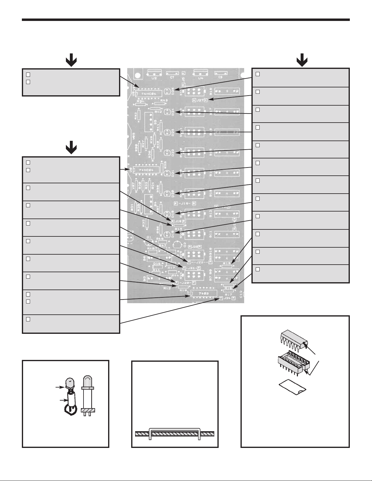
D25 - LED and Spacer
(see Figure B)
J27 - Jumper Wire
(see Figure C)
D24 - LED and Spacer
(see Figure B)
D23 - LED and Spacer
(see Figure B)
D22 - LED and Spacer
(see Figure B)
D21 - LED and Spacer
(see Figure B)
D20 - LED and Spacer
(see Figure B)
D19 - LED and Spacer
(see Figure B)
D18 - LED and Spacer
(see Figure B)
R19 - 1kΩ 5% 1/4W Resistor
(brown-black-red-gold)
R16 - 1kΩ 5% 1/4W Resistor
(brown-black-red-gold)
R17 - 1kΩ 5% 1/4W Resistor
(brown-black-red-gold)
U7 - IC socket 14-pin
U7 - 7403 IC
(see Figure D)
J24 - Jumper Wire
(see Figure C)
Figure B
Flat
Spacer
Mount with the flat side of the
LED as shown on the top
legend side of the PC board.
Figure C
Cut a piece of bare wire long
enough so that 1/4” of wire
passes through each hole in
the PC board after the wire is
formed (provided in the
second package).
-41-
Figure D
IC
Notch
Socket
Insert the IC socket into the PC board
with the notch in the direction shown
on the top legend. Solder the IC
socket into place. Insert the IC into the
socket with the notch in the same
direction as the notch on the socket.
Page 43
INSTALL COMPONENTS TO PC BOARD
SW4 - Slide Switch SW7 - Slide Switch SW10 - Slide Switch
Start Here
Continue
SW5 - Slide Switch SW8 - Slide Switch SW11 - Slide Switch
SW6 - Slide Switch SW9 - Slide Switch SW12 - Slide Switch
B7 - 4-pin Bredblox B11 - 4-pin Bredblox B15 - 4-pin Bredblox
B8 - 4-pin Bredblox B12 - 4-pin Bredblox B16 - 4-pin Bredblox
B9 - 4-pin Bredblox B13 - 4-pin Bredblox B17 - 4-pin Bredblox
B10 - 4-pin Bredblox B14 - 4-pin Bredblox B18 - 4-pin Bredblox
(see Figure F) SW13 - Slide Switch
(see Figure E)
Figure E
Hold the bredblox down flush to the PC
board from the top legend side and
solder the metal pins into place. Then,
melt the plastic pins with your soldering
iron to hold the plastic blocks in place as
shown.
Plastic Pins
Melted Pins
Mount the switch onto the legend side
of the PC board as shown. Flip the
board over and solder the part into
place. Be sure to keep the three
soldered sets of leads separate as
shown.
Figure F
Foil side of
PC board
Solder
Switch
Legend side
of PC board
INSTALL COMPONENTS TO FRONT PANEL
Interlock the bredboard to the bottom edge of the existing bredboard on the top panel as shown in Figure H.
Fasten the bredboards in place with two #4 x 1/4” AB black screws from the back side of the panel. Use the
holes on the 9426 bredboard as shown in Figure G. CAUTION: Do not remove the paper backing from the
bredboard.
Figure G
Bredboards
Use these
holes
Figure H
9426
9830
Note: The 9418 and the power strip 9408 make
up the 9426 bredboard.
Top Panel
#4 x 1/4” Screws
-42-
Page 44

RESISTANCE ANALYSIS OF DIGITAL SECTION
lace the top panel onto the unit. Static testing of the digital section circuits. Do not plug the power supply into
P
a 117 volt power source until all of the resistance readings check out. The values given below are
approximate.
From To Switch Position Ohms Resistance Measured
SW1 GND In down position less than 1Ω
SW2 GND In down position less than 1Ω
SW3 GND In down position less than 1Ω
SW4 GND In down position less than 1Ω
SW5 GND In down position less than 1Ω
SW6 GND In down position less than 1Ω
SW7 GND In down position less than 1Ω
SW8 GND In down position less than 1Ω
SW1 GND In up position greater than 3kΩ
SW2 GND In up position greater than 3kΩ
SW3 GND In up position greater than 3kΩ
SW4 GND In up position greater than 3kΩ
SW5 GND In up position greater than 3kΩ
SW6 GND In up position greater than 3kΩ
SW7 GND In up position greater than 3kΩ
SW8 GND In up position greater than 3kΩ
SW1 +5V In up position less than 300Ω
SW2 +5V In up position less than 300Ω
SW3 +5V In up position less than 300Ω
SW4 +5V In up position less than 300Ω
SW5 +5V In up position less than 300Ω
SW6 +5V In up position less than 300Ω
SW7 +5V In up position less than 300Ω
SW8 +5V In up position less than 300Ω
LOGIC SW
XX
YY
DATA SWITCHES
SW1 SW2 SW3 SW4 SW5 SW6 SW7 SW8
-43-
Page 45
VOLTAGE ANALYSIS OF DIGITAL SECTION
lug the power supply into a 117 volt power source. The values given below are approximate.
P
From To Switch Position Volts Volts Measured
X GND In up position 5V
X GND In up position less than 1V
Y GND In up position 5V
Y GND In up position less than 1V
SW1 GND In up position 5V
SW2 GND In up position 5V
SW3 GND In up position 5V
SW4 GND In up position 5V
SW5 GND In up position 5V
SW6 GND In up position 5V
SW7 GND In up position 5V
SW8 GND In up position 5V
X GND In down position less than 1V
X GND In down position 5V
Y GND In down position less than 1V
Y GND In down position 5V
SW1 GND In down position less than 1V
SW2 GND In down position less than 1V
SW3 GND In down position less than 1V
SW4 GND In down position less than 1V
SW5 GND In down position less than 1V
SW6 GND In down position less than 1V
SW7 GND In down position less than 1V
SW8 GND In down position less than 1V
High Positions
XX
YY
LOGIC SW
XX
YY
SW1-8
DATA SWITCHES
SW1 SW2 SW3 SW4 SW5 SW6 SW7 SW8
-44-
Page 46

TESTING THE DIGITAL SECTION
TESTING THE LOGIC INDICATOR FUNCTION
here are eight logic indicators which you will be checking out. Put a wire to the 5V power supply and touch
T
the “A” logic indicator test pin. The “A” LED should light up. Remove the wire and the LED should go out. Do
the same for the B, C, D, E, F, G and H pins.
TESTING THE LOGIC SWITCHES
There are two logic switches and four conditions to be checked out. Connect a wire from the “X” test pin to the
“A” logic indicator test pin. Connect another wire to the “X” test pin to the “B” test pin.
Apply power and note that the “A” LED indicator should be lit when the logic switch is in the “X” position and the
“B” LED should light and the “A” LED not light. Check the “Y” logic switch in the same manner.
TESTING THE DATA SWITCHES
There are eight data switches to be checked. The output of the switches are 5V or ground depending on the
position. Connect a wire to the SW1 test pin and the “A” test pin. The “A” LED should light when the switch is
placed toward the top of the case. Repeat the same test on SW2, SW3, SW4, SW5, SW6, SW7 and SW8.
Unplug the unit from the AC outlet.
DIGITAL TROUBLESHOOTING CHART
PROBLEM POSSIBLE CAUSE
No +5V on data switch terminals. 1. Measure for a DC voltage of +5V across R15.
A. Check R15, J19, J23 and J13.
B. Switch shorted to ground.
LED doesn’t light 1. Check that the LED is in correctly.
2. Check the input and output resistors.
3. Measure input for +5V and output at ground.
A. Short to ground or defective IC.
LED always on 1.Measure for zero voltage voltage at input pin.
A. Pin shorted or defective IC
2. Measure voltage to output pin for +5V.
A. Pin shorted or defective IC.
Logic switch terminal always high 1. Check that input resistor is grounded.
A. Bad ground connection or switch.
2. Measure for +5V on R16 - R19.
A. Check resistor.
3. Defective IC.
-45-
Page 47

FINAL ASSEMBLY
Fasten the front panel in
place with four #6 x 3/8”
thread cutting screws, as
shown in Figure I.
Knobs
Nuts 8mm
Figure I
Washers 9mm
Nut 7mm
Fasten the PC board to
the spacer on the front
panel with a fiber washer
and a 4-40 x 1/4” screw
(from Power Supply
Section) from the foil side
of the PC board, in the
location shown in Figure J.
Fastenthe pots to the front
panel with an 8mm washer
and a 7mm nut, as shown
in Figure I.
Turn the shafts on the two
switches fully counterclockwise. Push the
knobs onto the shafts so
that the line on the knob is
in line with the
“Squarewave” on the
waveform control and “10”
on the Coarse Frequency
control (see Figure K).
If the knobs are loose on
the shafts, insert a
screwdriver into the slot
and expand the slot
slightly (see Figure M).
Washer 8mm
Nuts 7mm
Washers 8mm
#6 x 3/8” Thread
Cutting Screws
#6 x 3/8” Thread
Cutting Screws
Turn the shafts on the pots fully counter-clockwise. Push the knobs onto the shafts so that the line on the
knob is in line with the end of the circle on the front panel, as shown in Figure L.
If the knobs are loose on the shafts, insert a screwdriver into the slot and expand the slot slightly (see Figure M).
4-40 x 1/4” Screw
Fiber Washer
100
10
WAVE FORM COARSE FREQ
10k
100k
1k
Figure K
Figure J
Figure L
Figure M
-46-
Page 48

INSTALL COMPLETED UNIT INTO CASE
Tie a knot in the line cord 12” from the switch location. Feed the line cord between the cross bracket and the
PC board.
Locate the line cord hole in the case (see Figure N). Insert the line cord into the hole through the slot. To
open up the slot, press down on one side of the slot (see Figure O). Insert the bushing into the hole and
pull on the line cord until the slot is snug against the bushing.
O
Insert the unit into the case at a 45
x 1/2” black screws in the corner holes of the panel.
The line can be neatly stored in the bin shown in Figure N. Gather up the line cord and insert it into the bin.
Insert the line cord fastener into the slots to the hole in place, as shown in Figure P.
Place the label on the front of the case with the top of the label facing away from the handle, as shown in
Figure Q.
angle with the bottom edge first. Secure the unit into place with four 8
Figure N
Figure Q
Figure O
Figure P
-47-
Page 49

CIRCUIT DESCRIPTION - DIGITAL SECTION
THE DATA SWITCHES
here are eight data switches labeled SW1 through SW8. The circuit is very simple. To perform the desired
T
functions, there is a double throw double pole switch, wired as a single pole double throw. One end is connected
to the 5V, the other to ground and the center lug is connected to the output.
THE LOGIC SWITCHES
The logic switches are also DPDT switches wired as SPST switches. The logic switches perform the same
function as the data switches. That is, they produce high or low states. But there is one big difference. When
switching the data switches, many pulses may be produced due to bouncing of the contacts.
In the logic switches, only one pulse is produced at the IC output no
matter how many times the contacts bounce. This is extremely
important if you are producing pulses for counting circuits. Figure R
shows the wiring of the logic switch. The two NAND gates are connected
so that when the X input is grounded, the X output goes high. Opening
and closing the ground at X will not change the output. Only when X is
grounded will the output change to low. Thus, only one output change is
produced with one movement of the X switch. There are two outputs
from each logic switch, X and X or Y and Y.
THE LOGIC INDICATORS
There are eight logic indicators. Figure S shows the circuit. It consists of
a 74HC04 IC. When the input is over 2.8V, the output of the IC will be low,
drawing current through the LED indicator. The 120Ω resistor limits the
current in the LED to less than 20mA. When there is no connection to the
input of the logic indicators, the two 100kΩ resistor bias the input to GND.
This insures that the LED will be off.
X
X
100k
1
IC7
2
IC7
4
5
3
6
Figure R
100k 120
74HC04
Figure S
LED
X
X
5V
-48-
Page 50

SCHEMATIC DIAGRAM
-49-
Page 51

QUIZ - DIGITAL SECTION
NSTRUCTIONS: Complete the following examination, check your answers carefully.
I
1.The logic switches consist of . . .
A. two NAND gates and an SPST switch.
B. three OR gates.
C. two NAND gates and a DPDT switch.
D. one OR gate.
2.When the logic switch is thrown . . .
A. the contacts do not bounce.
B. a single transition is produced at the NAND gate output.
C. a multiple transition is produced at the NAND gate output.
D. none of the above.
3. If the X output is high, opening and closing the ground at X switch will . . .
A. cause the X output to go low.
B. cause the X output to go high.
C. cause the X output to go from high to low.
D. none of the above.
4.The logic indicator LED lights up when . . .
A. input voltage is 2V.
B. input voltage is greater than 2.8.
C. the IC output is high.
D. all of the above.
5.The logic switches use . . .
A. single pole single throw switches.
B. double pole double throw switches wires as single pole double throw switches.
C. two pole 5 position rotary switches.
D. 4 pole 3 position rotary switches.
6.The 100kΩ resistor on the logic indicator input . . .
A. divides the input voltage in half.
B. bias the input to +5V.
C. bias the input to GND.
D. turn on the LED.
7. When the logic switch is in the X position . . .
A. X is high, X is low.
B. X is high, X is high.
C. X is low, X is high.
D. X is low, X is low.
8. When the data switch is up and connected to the logic indicator . . .
A. the switch output is greater than 2.8V.
B. the switch output is GND.
C. the LED will be out.
D. none of the above.
9.The +5VDC power for the digital section comes from a . . .
A. 7805 IC.
B. 7905 IC.
C. 5V battery.
D. 7812 IC.
10. If pin 4 on U7B is high . . .
A. pin 3 is low.
B. pin 1 is low.
C. pin 2 and 6 are high.
D. pin 5 is high.
Answers: 1. C; 2. B; 3. D; 4. B; 5. B; 6. C; 7. A; 8. A; 9. A; 10. B
-50-
Page 52

Elenco®Electronics, Inc.
150 Carpenter Avenue
Wheeling, IL 60090
(847) 541-3800
Web site: www.elenco.com
e-mail: elenco@elenco.com
 Loading...