

Page 1

DIGITAL / ANALOG TRAINER
MODEL XK-150
A COMPLETE MINI-LAB FOR BUILDING,TESTING
AND PROTOTYPING ANALOG AND DIGITAL CIRCUITS
Elenco Electronics, Inc.
Instruction Manual
Copyright © 1998 Elenco Electronics, Inc. Revised 2001 REV-C 753273
Page 2
Qty Description Part #
1 Transformer 440111
1 PC Board digital 514000
1 PC Board analog 514001
2 PC Board 1k, 100k POT 514002
1 Fuse .25A 531005
9 Switch Slide 2P2T (SW5 - 13) 541023
1 Switch Slide 2P3T (SW4) 541208
1 Switch Rocker (SW1) 541209
7 Connector 4-pin 591104
1 Connector 3-pin 596032
3 Heat Sink 615005
8 Spacer Nylon 624117
1 Socket IC 8-pin 664008
2 Socket IC 14-pin 664014
1 Socket IC 16-pin 664016
5 Knob Push-on 622017
1 Plastic Case top/bottom 623027
1 Bushing Strain 624002
Qty Description Part #
2 Binding Post Black 625031
6 Nut Binding Post 625031HN
6 Lockwasher Binding Post 625031LW
2 Binding Post Red 625032
2 Binding Post Yellow 625034
6 Screw M3 x 10mm 642358
13 Screw #4 x 5/16” AB Phil 642442
5 Nut Pot 7mm 644101
5 Nut 3mm x .5 644104
2 Washer Flat #4 645000
5 Washer Flat 7mm x 12mm 645111
2 Lockwasher #4 INT 646401
4 Feet Rubber 662003
1 Fuse Holder Assembly 663005,LB,UB,W,N
1 Label XK-150 Case 723100
1 Line Cord 862105
2 Switch Slide 2P2T (SW2 - 3) 920000
Qty Symbol Description Part #
9 D1 - 9 1N4001 Diode 314001
2 ZD1 - 2 Zener Diode 1N5234B 315235
9 Q1 - 9 2N3904 Transistor 323904
1 IC2 LM317 IC 330317
1 IC3 LM337 IC 330337
Qty Symbol Description Part #
1 IC7 555 IC 330555
1 IC4 XR2206 332206
1 IC1 LM7805 IC 337805
9 LD1 - 9 LED Red 350002
2 IC5, IC6 74LS03 IC 37LS03
-1-
PARTS LIST
RESISTORS
Qty Symbol Description Color Code Part #
11 R15, 23, 26, 29, 32, 35, 38, 43, 46, VR6-7 150Ω 5% 1/4W brown-green-brown-gold 131500
1 R9 200Ω 5% 1/4W red-black-brown-gold 132000
1 R22 470Ω 5% 1/4W yellow-violet-brown-gold 134700
2 R4, R2 470Ω 5% 1/2W yellow-violet-brown-gold 134701
8 R8, 12, 13, 14, 16, 18, 19, 17 1kΩ 5% 1/4W brown-black-red-gold 141000
1 R1 2.2kΩ 5% 1/4W red-red-red-gold 142200
1 R3 2.7kΩ 5% 1/4W red-violet-red-gold 142700
1 R20 15kΩ 5% 1/4W brown-green-orange-gold 151500
17 R7, 24, 25, 27, 28, 30, 31, 33, 34, 18kΩ 5% 1/4W brown-gray-orange-gold 151800
36, 37, 39-42, 44, 45
1 R10 43kΩ 5% 1/4W yellow-orange-orange-gold 154300
1 R11 47kΩ 5% 1/4W yellow-violet-orange-gold 154700
1 R21 62kΩ 5% 1/4W blue-red-orange-gold 156200
1 VR4 1kΩ POT 192439
2 VR1, VR2 2kΩ POT 192438
1 VR5 100kΩ POT 192638
1 VR3 1MΩ POT 192738
CAPACITORS
Qty Symbol Description Part #
1 C17 10pF (10) Discap 211011
1 C12 68pF (68) Discap 216816
1 C7 470pF (470) Mylar 224717
1 C8 .0047µF (472) Mylar 234717
1 C13 .01µF (103) Mylar 241017
2 C9, 15 .1µF (104) Discap 251010
5 C4, 5, 6,10,11 10µF 25V Electrolytic Radial 271045
4 C1, 2, 3, 14 1,000µF 25V Electrolytic Radial 291045
SEMICONDUCTORS
MISCELLANEOUS
Page 3

GENERAL SPECIFICATIONS FOR MODEL XK-150
Power Supplies:
• +1.25V to 15VDC @ .25 amp
• -1.25 to -20VDC @ .25 amp
• +5V +
5% @ .5 amp
• 30V AC center tapped at 15VAC @ .25 amp.
• Load regulator all DC supplies less than .2V no load to .25A
• Line regulator all DC supplies less than .2V 105 to 135V
• Hum and ripple all DC supplies less than .01V RMS
• Short protection all DC supplies-Inter nal IC ther mal cutoff
• Fuse - .25A 250V
Function Generator Analog Section:
• Waveforms sine, square, complimentary square
• Frequency - adjustable from 200 - 40kHz in 2 ranges
• Amplitude - sine wave 4Vpp
square wave 12Vpp
• Output impedance 600Ω:
Digital Section:
• Data switches, eight DPDT, Hi 5V, low 0V
• Logic switches, two no bounce with complimentary output
“On” voltage level 2.8V min., “Off” voltage level 1V max.
Input impedance 100kΩ.
• Eight LED readouts, 100kΩ input impedance
• Clock frequency, 1Hz,1kHz, 100kHz, 60Hz
• Clock amplitude, 5Vpp squarewave
• Clock rise time, better than 100nsec.
Bredboards Section:
• One bredboards containing 830 tie points including to bus strips
Variable Resistance (undedicated):
• 1kΩ Potentiometer
• 100kΩ Potentiometer
-2-
Page 4
-3-
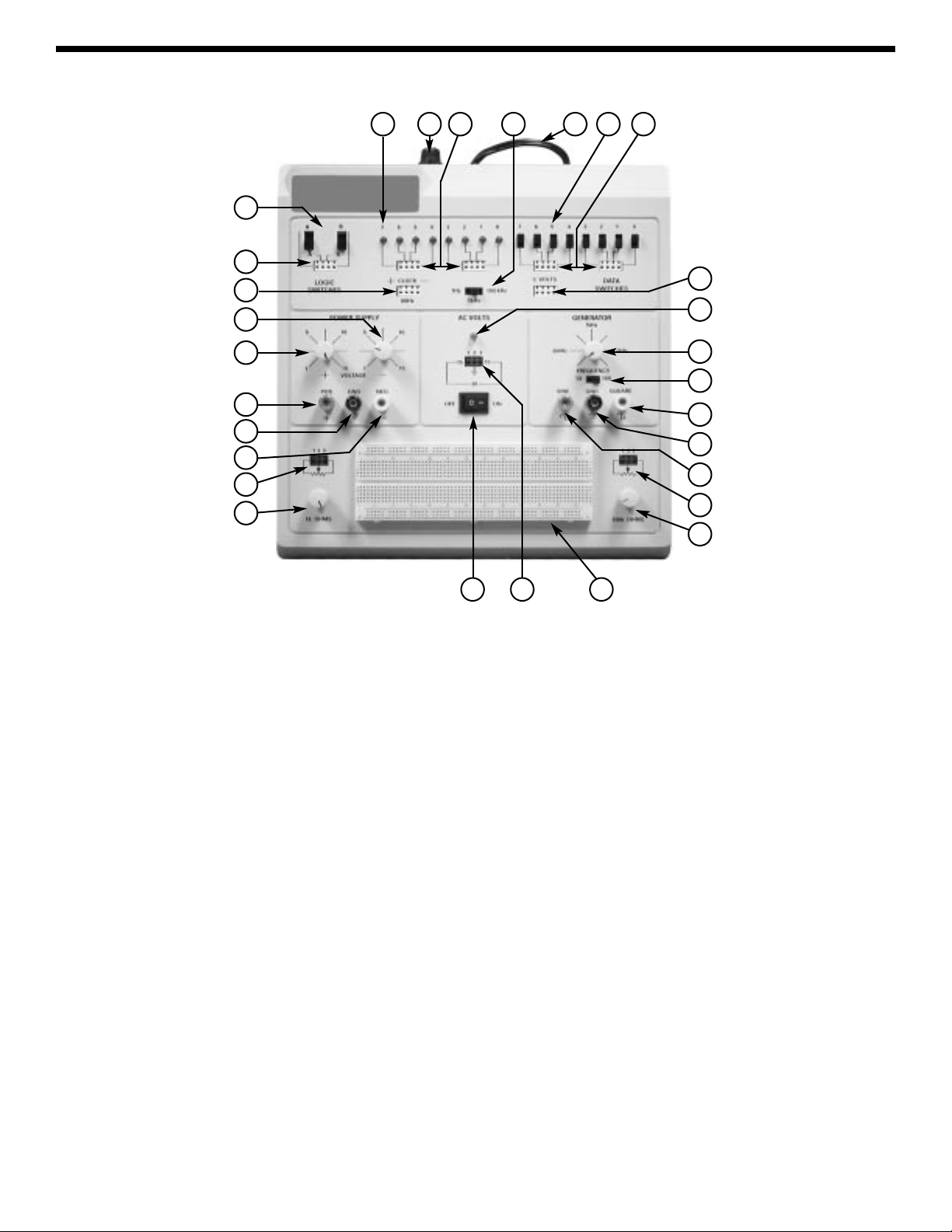
USERS DESCRIPTION OF FRONT PANEL CONTROL
1) 1kΩ undedicated potentiometer.
2) Output Terminals for 1kΩ undedicated potentiometers.
3) Output Terminals for -15V power supply.
4) Gnd Terminals for the +/-15 variable power supply.
5) Output Terminals for +15V power supply.
6) Variable Positive Voltage Control - Varies positive voltage from 1.25 to 15V at indicated output terminal.
7) Variable Negative Voltage Control - Varies negative voltage from -1.25 to -15V at indicated output connector pin.
8) Output Terminals for the Clock frequencies.
9) Output Terminals for the logic switches.
10)
Two Logic Switches - These are no bounce logic switches. Give one signal state change per movement of switch.
11) Logic Indicators LEDs, total eight.
12) Fuse Holder - Easy access for replacement of .25A 250V fuse.
13) Input Points For Logic Indicator LEDs. “0” input corresponds with 0 lamp, etc.
14) Selects CLOCK frequency range 1Hz,1kHz, and 100kHz.
15) Power Cord.
16) Eight Data Switches - Lets output of 5V or 0V depending on position.
17) Output Terminals For the DATA Switches 0-1.
18) Output Terminal for +5V power supply.
19) Power ON LED, Lights When Unit is ON.
20) Frequency Control - allows easy selection of desired function generator frequency.
21) Frequency Multiplier Switch. range from X1 (200 to 2,000Hz) or X100 (2,000 to 20,000Hz).
22) Output Terminals for SQUARE wave.
23) Gnd Terminals for SINE and SQUARE wave.
24) Output Terminals for SINE wave.
25) Output Terminals for 100kΩ undedicated potentiometers.
26) 100kΩ undedicated potentiometer.
27) One Bredboard containing a total of 830 tie points including 2 independent bus lines.
28) Power Output Terminals - This provides 30VAC center tapped at 15VAC -
29) ON-OFF Switch - Allows power to be applied to all outputs. LED will light when on.
9
10
8
7
6
5
4
3
1
2
11 12 13 14 15 16 17
18
19
20
21
22
24
25
26
23
27
2829
Page 5

-4-
INTRODUCTION
Congratulations on your purchase of the Elenco Model XK-150 Digital / Analog Trainer. This trainer is designed
to simplify designing of digital and analog circuits. It contains most of the necessary test equipment needed to
build and test these circuits.
Your XK-150 has four basic trainers in a single package. They are, 4 independent power supplies, an analog
trainer, a digital and a bredblock assembly trainer. We shall proceed in describing each trainer in the following
sections.
POWER SUPPLY
Model XK-150 has four built-in power supplies which will satisfy most design needs. There are two variable power
supplies giving up to +15 volts and -15 volts at .25 amp. The two other supplies consists of a fixed +5V at .25 amp,
and a 30VAC center-tapped at 15VAC at .25 amp. All the DC supplies are regulated to within 150mV. This means
that you can increase the current draw from no load to .25 amp and the voltage will change less than 150 millivolts.
The supplies are also short circuit protected by using integrated circuit regulator devices.
ANALOG TRAINER SECTION FUNCTION GENERATOR
The analog trainer contains a function generator capable of producing sine and square waveform. The frequency of
this generator is variable in two ranges from 200 hertz to 20,000 hertz.The output voltage amplitude for the sine w a v e
is 4Vpp and the square wave at 12Vpp. The output impedance is approximately 600 ohms.
DIGIT AL TRAINER SECTION
The digital trainer has the necessary functions to do your digital designs. They consist of a clock generator, two
no bounce logic switches, 8 LED indicator lamps and 8 data switches. These functions will make it easy to do
your digital experiments.
Page 6

-5-
TESTING THE XK-150 DIGITAL ANALOG TRAINER
The following paragraphs give detailed instructions on testing the digital / analog trainer.
Note that in the XK-150 trainer there are five major functions, (1) Power Supply (2) Logic Indicators (3) Function
Generator (4) Logic Switches and (5) Data Switches. We shall proceed in testing out each section.
POWER SUPPLY TESTING
Plug the trainer into 120VAC outlet and set the power switch to the “ON” position. The red LED will light when
the unit is on. Set the the knobs for the +15 and --15 volts fully counter clock wise. Obtain a digital voltmeter
and measure the voltage at POS (+15V) binding post. The voltage should be approximately 1.25 volts .Measure
the voltage at the NEG (--15V) binding post. The voltage should be approximately --1.25 volts. Then turn both
knobs fully clockwise and measure the outputs again. The outputs voltage should be between 14.5 to 16 volts.
Short the POS binding post or the NEG binding post to the GND binding post. DO NOT short the positive and
negative posts together. The voltage regulators will turn off and the voltage drops to zero. Remove the shorts
and voltage should recover.
Set the +15 volt supply to 15 volt.If you have a 60 ohm 4 watt resistor, place it across the POS and GND binding
posts. The output of the 15V supply should not change more than .15 volts. In making this test, the voltmeter
leads should be clipped to the terminal directly and not to the load leads. This is to prevent errors in voltage drop
due to contact resistance of the load. Do the same for the -15V output, connecting the resistor between the NEG
and GND binding posts.The output should not change more than .15 volts.
Measure the voltage at the +5V output.The voltage should read between 4.75 and 5.25 volts. Short the output
to the GND binding post.
The voltage regulators will turn off and the voltage drops to zero. Remove the short
and voltage should recover.
Place
a 20Ω, 2 watt resistor from the output to the GND binding post and measure
the voltage. Again, the output should not change more than .15 volts.
Set you meter to measure AC volts. Measure the AC voltage across the 1 and 3 terminal of the ac output. The
voltage should be about 30VAC. Move one of the leads to the 2 terminal the the voltage should be about 15VAC.
WARNING!! DO NOT SHORT THE AC OUTPUT TO GND.
TESTING THE FUNCTION GENERATOR
To test the function generator, you will need an oscilloscope. Connect the scope to the SINE wave binding post
and the ground clip to the GND binding post. Set the switch the to 1X position. Your scope should show a sine
wave with an output of about 4Vpp. Turn the frequency control, the frequency should vary between 200 and
2000 hertz. Turn the switch to 10X and vary the frequency control. The frequency should vary between 2,000
and 20,000 hertz. Check the square wave output in the same manner. The amplitude of should be 12Vpp.
TESTING THE CLOCK
If your scope is a dual trace, connect one probe to the +CLOCK terminal and the other to the --CLOCK terminal.
Set the switch the 1kHz. You will note the two frequencies are 180 degrees out of phase. Check the 1kHz and
100kHz settings. Check the 60Hz terminal a for 60Hz square wave signal.
If no scope is available, connect a wire from the +CLOCK terminal to the “7” LED logic indicator terminal.
Connect another wire from the --CLOCK terminal to the “6” LED logic indicator. Set the clock frequency switch
to 1 hertz. The two LEDs should blink alternately. In the 1kHz and 100kHz position, both LEDs will be on.
Remove the wire from the +CLOCK terminal and connect it to the 60Hz terminal. The LED should be on.
Page 7

-6-
TESTING THE LOGIC INDICATOR FUNCTION
There are eight logic indicators which you will be testing. Place a wire to the 5V terminal and touch the “0” LED
logic indicator terminal. The “0”LED should light up. Remove the wire and the LED should go out. Do the same
for the 1, 2, 3, 4, 5, 6 and 7 logic terminals.
TESTING THE LOGIC SWITCHES
There are two logic switches and four conditions to be tested. Connect a wire from the “A” terminal to the “7” LED
logic indicator terminal. Connect another from the “A” ter minal to the “6” LED logic indicator terminal.
Note that the “7” LED logic indicator should be lit when the logic switch is in the “A” positions and the “6” LED
is not lit. Moving the logic switch to “A” should reverse the indicator LEDs, that is the “6” LED should light and
the “7” LED not light. Check the B logic switch in the same manner.
TESTING THE DA TA SWITCHES
There are eight data switches to be tested. When the switch is in the up position, the output is at 5V. When the
switch is in the down position, the output is at ground. Place all the switches in the down position. Connect a
wire from the SW0 terminal and the “0” LED terminal. The “0” LED should light when the switch is placed toward
the top case. Repeat the same test on SW1, SW2, SW3, SW4, SW5, SW6 and SW7.
This completes the testing of the trainer.
CIRCUIT DESCRIPTION
The XK-150 Power Supply features two variable output voltages and a fixed 5V. The variable voltages are 1.25V
to 15V and --1.25 to --15V at up to .25 ampere maximum current. All supplies are regulated to better than .2V when
going from no load to full load. Varying the input AC voltage from 105 to 135V will have practically no effect on the
output voltages. This is because of the specially designed IC circuits used in the XK-150 circuits. Severe
overloading or even shorting the output circuits will not damage the supplies. Special tur n-off circuits in the IC
sense the overload and turn off the output.
THE POSITIVE 1.25 TO 15V POWER SUPPLY
Figure 1 shows a simplified circuit diagram of the positive supply. It consists of a power transformer, a DC
rectifier stage and the regulator stage.
TRANSFORMER
The transformer T1 serves two purposes. First, it reduces the 120VAC input to 34VAC to allow the proper
voltage to enter the rectifier stages. Second, it isolates the power supply output from the 120VAC line. This
prevents the user from dangerous voltage shock should he or she be standing in a grounded area.
Figure 1
Simplified diagram of positive power supply
120VAC
Input
17VAC 20VDC
1.25 - 15V
Regulated
Output
Transformer
120V to 17V
AC to DC
Converter
Voltage
Regulator
Page 8

AC T O DC CONVERTER
The AC to DC converter consists of diodes D1, D2 and capacitor C1. Transformer T1 has two secondary
windings which are 180 degree out of phase. The AC output at each winding is shown in Figure 2A and 2B.
Diodes are semiconductor devices that allow current to flow in one direction. The arrow in Figure 3 points to the
direction current will flow. Only when the transformer voltage is positive will current flow through the diodes. Figure
3 shows the simplest possible rectifier circuit. This circuit is known as a half-wave rectifier . Here the diode conducts
only half of the time when the AC wave is positive as shown in 2C. Use of this circuit is simple but inefficient. The
big gap between cycles require much more filtering to obtain a smooth DC voltage.
By the addition of a second diode and transformer
winding we can fill in the gap between cycles as
shown in Figure 4. This circuit is called full-wave
rectification. Each diode conducts when the voltage is
positive. By adding the two outputs, the voltage
presented to capacitor C1 is more complete, thus
easier to filter, as shown in Figure 2E. When used in
60 cycles AC input power, the output of a full wave
rectifier will be 120 cycles.
Capacitor C1 is used to store the current charges,
thus smoothing the DC voltage. The larger the
capacitor, the more current is stored. In this design
1000µF capacitors are used, which allows about 1
volt AC ripple when .25A is drawn.
In practice, the current through the diodes is not as
shown in Figure 2C. Because capacitor C1 has a
charge after the first cycle, the diode will not conduct
until the positive AC voltage exceeds the positive
charge in the capacitor. Figure 5 shows a better
picture of what the current flow looks like assuming
no loss in the diode.
It takes a few cycles for the voltage to build up on the capacitor . This depends on the
resistance of the winding and diode. After the initial start-up, there will be a charge
and discharge on the capacitor depending on the current drawn by the output load.
Remember, current only flows through the diodes when the anode is more positive
than the cathode. Thus, current will flow in shor t bursts as shown in Figure 5.
The DC load current may be .25A but the peak diode current may be three times
that. Therefore, the diode rating must be sufficient to handle the peak current.
The IN4001 has peak current rating of 10 amps.
REGULATOR CIRCUIT
The regulator circuit in the Model XK-150 power supply consists of a LM-317
integrated circuit. This IC is specially designed to perform the regulation
function. Figure 6 shows a simplified circuit of how the LM-317 IC works.
Transistors Q1 and Q2 form a circuit known as a differential amplifier. Transistor
Q1 base is connected to a stable 1.5V reference voltage. The base of Q2 is
connected to the regulator output circuit through a voltage divider network. The
collector of transistor Q2 is connected to a current source. This basically is a PNP
transistor biased to draw about 1mA current. Transistor Q2 sees the current
source as a very high resistor of about 1 meg ohms. Thus, the gain of transistor
Q2 is extremely high.
Figure 2
Figure 3
Figure 4
Figure 5
Figure 6
-7-
Voltage Waveform for Supply
A) Transformer
Winding AB
B) Transformer
Winding BC
C) Output of
diode D1.
D) Output of
diode D2.
E) Total of diodes
D1 & D2.
20V
F) Output of capacitor C1
Ripple depends on load
current (expanded).
Half Wav e Rectifier
Full Wav e Rectifier
A) Transformer
Winding
B) Voltage C1
C) Current
through diodes
20V
Peak
20V
2V
Output
R1
R2
Divider
Q1
Q2
1.5V
Q3
Q4
Q5
Current
Source
Equalized
to 1 Meg.
Page 9

-8-
Transistor Q5 is called the pass transistor. It controls the current reaching the output. Transistor Q3 and Q4 are
emitter followers. Their function is to raise the impedance of the pass transistor .Note that transistor Q2, Q3, Q4,
Q5 and resistor R1 form a close loop. Also note that the feedback to the base of Q2 is negative, that is, when
the base of Q2 goes positive, the output at emitter Q5 goes negative. Now if the 2V output voltage goes down
because of current drain at the output, the base of Q2 will drop forcing the the collector v oltage of Q2 to go higher .
This will bring the output voltage back to 2V. This is the basis of all negative feedback regulators.
Another feature of the LM-317 regulator is to protect the IC against overload and output shorts. If the IC is
overloaded, the junction of an ov erload transistor will overheat. A transistor will sense this overheating and shut
down transistor Q5.
The LM-317 IC is basically a 1.25 regulator. To be able to vary the output
1.25 to 15V we stack the IC on a DC voltage as shown in Figure 6A. When
VR1 equals 0, the output voltage is 1.25V as determined by the LM-317 IC.
Note that the voltage across R1 is always 1.25 volts. When R1 equals VR1,
the voltage across VR1 will equal the 1.25 volts across R1, therefore the
output voltage will be 2.5 volts. When VR1 is 5 times R1, the output voltage
is 6.25 volts. As you can see, varying resistor VR1 will vary the voltage from
1.25 to 15V.
THE NEGATIVE VOLTAGE REGULATOR
The theory of the voltage regulator is the same as the previously discussed positive regulator. The basic
difference is that diodes D1 and D2 are reversed producing a negative v oltage across capacitor C1. The LM-337
IC is designed to operate from a negative supply.
THE DATA SWITCHES
There are eight data switches labeled “0” to “7”. The circuit is very simple. To perform the desired functions
there is a double throw-double pole switch. One end is connected to the 5V, the other to ground and the center
lug is connected to the output.
THE LOGIC SWITCHES
The logic switches perform the same function as the data switch, that is, they produce high or low states. But
there is one big difference. When switching the data switches, many pulses may be produced due to bouncing
of the contacts.
In the logic switches, only one pulse is produced, no matter how many
times the contacts bounce. This is extremely important if you are
producing pulses for counting circuits. Figure 7 shows the wiring of the
logic switch. The two NAND gates are connected so that when A input
is grounded the output A goes high. Opening and closing the ground
at A will not change the output. Only when A is grounded will the
output change to low. Thus, only one output change is produced with
one movement of the A switch. There are two outputs from logic
switch, A and A or B and B.
THE FUNCTION GENERATOR
The function generator frequencies are produced by an XR-2206 integrated circuit. This IC is capable of
producing high quality sine and square waveform of high stability and accuracy. Figure 8 shows the block
diagram of the XR-2206 IC.
Figure 6A
Figure 7
1.25 - 15V
R1
VR1
LM-317
A
A
A
A
6
5
4
1
2
3
Page 10

The XR-2206 is comprised of four functional blocks, a voltage
controlled oscillator (VCO), an analog multiplier & sine shaper, a
unity gain buffer amplifier and a set of current switches.
The VCO actually produces an output frequency proportional to
an input current. Across pins 5 and 6, two timing capacitor are
switched between to give different frequency ranges. On pin 7,
the 1MΩ variable resistor controls the actual frequency output.
These two components form the RC time constants for the
oscillator frequency.
The VCO produces a square wave signal. This square wave is
sent to a shaper and converted into a sine wave.
THE LOGIC INDICATORS
There are eight logic indicators. Figure 9 shows the circuit. It consists of a
transistor, LED, and three resistors. The two 18kΩ resistors form a voltage divider.
When the input is over 1.4V, the transistor will turn on allowing current to flow
through the LED to ground, thus turning it on. The 150Ω resistor limits the current
in the LED to about 30mA.
Figure 9
-9-
WARRANTY POLICY
Your XK-150 Digital / Analog Trainer has been tested and conforms to our rigid requirements on performance and durability. It is
guaranteed to be free of defects in workmanship, materials and construction for a period of 2 years. If this product should fail during
normal use within the first 3 months from the date of purchase, Elenco will repair or replace the unit at no cost. For the remainder of the
warranty period, a nominal service charge is required to cover shipping and handling.
When returning merchandise for repair, please include proof of purchase, a brief letter of explanation of problem and sufficient packing
material. Before returning any merchandise, please call our service department at (847) 541-3800 to obtain a return authorization
number (RA).
Elenco Electronics, Inc. Service Department
150 W. Carpenter Avenue Wheeling, IL 60090
Input
Vcc
150
LED
18k
18k
1
16
215
314
413
512
611
710
89
Symmetry
ADJ.
Waveform
ADJ.
Ground
Sync
Output
Bypass
FKS
Input
Timing
Resistor
Timing
Capacitor
V+
Mult. Out
Sine/Saw
Output
AM Input
+1
Multiplier
and
Sine
Shaper
VCO
Current
Switches
Figure 8
Page 11

-10-
SCHEMATIC DIAGRAM
Page 12

Elenco Electronics, Inc.
150 W. Carpenter Avenue
Wheeling, IL 60090
(847) 541-3800
http://www.elenco.com
e-mail: elenco@elenco.com
 Loading...