

Page 1

MULTI-NETWORK CABLE TESTER KIT
MODEL TCT-255K
Copyright © 2013, 2001 by ELENCO®All rights reserved. REV-D 753089
No part of this book shall be reproduced by any means; electronic, photocopying, or otherwise without written permission from the publisher.
ELENCO
®
Assembly and Instruction Manual
Page 2

GENERAL DISCUSSION
You can see a block diagram of the TCT-255 in Figure 1 below.
The TCT-255 Cable Tester has five basic blocks:
1. Power Supply
It powers all of the circuits of the tester (not including the terminator). The power supply has a low battery
indicator (less than 7.5V) and a circuit to disconnect power 30 - 50 seconds after the last push on the
test switch.
2. Oscillator
Uses a 555 timer IC with two resistors and one capacitor. They control the free running frequency and
duty cycle.
3. Step Pulses with Counter
The outputs change by the positive pulses from the test button switch.
4. Switches and LED Indicator
It includes eight electronic switches for operating the indicators (16 LEDs).
5. Terminator
Connected to cable under test. Identifies the polarity signals.
Cable Tester TCT-200 Termina tor LD-10 0
Figure 1
COUNTER SWITCHES
INPUT & OUTPUT
CONNECTORS
INPUT & OUTPUT
CONNECTORS
STEP PULSES
OSCILLATOR
LED
INDICATOR
CIRCUIT
IDENTIFY
POLARITY
POWER
SUPPLY
-1-
The TCT-255 Cable Tester is a convenient
instrument for testing different unshielded wiring
schemed communication cable with RJ-11 and RJ45 connectors and coax cable. This tester can be
used for testing cables before and/or after they are
installed. The tester offers easy operation by having
to push only one button. Testing status is indicated by
multiple LEDs and an auto power-off function
maximizes battery life.
The unique design of the TCT-255 allows you to
place the parts over their corresponding symbol in
the schematic drawing on the surface of the PC
board during assembly. This technique maximizes
the learning process while keeping the chances of
an assembly error at a minimum. It is very
important, however, that good soldering practices
are used to prevent bad connections.
The actual assembly is broken into SEVEN
SECTIONS. After each assembly, you will be
instructed to make certain tests and measurements
to prove that each section is functioning properly.
The theory for each section, or stage, should be
read before the test is started. This will provide the
student with an understanding of what that stage
has been designed to accomplish, and how it
actually works. If a test fails to produce the proper
results, a troubleshooting guide is provided to help
you correct the problem. For testing you need to
have only a voltmeter for measuring DC and AC.
INTRODUCTION
Page 3

-2-
Warning:
If the capacitor is
connected with
incorrect polarity, it
may heat up and
either leak, or
cause the capacitor
to explode.
IDENTIFYING RESISTOR VALUES
Use the following information as a guide in properly identifying the value of resistors.
BANDS
METRIC UNITS AND CONVERSIONS
Abbreviation Means Multiply Unit By Or
p Pico .000000000001 10
-12
n nano .000000001 10
-9
µ micro .000001 10
-6
m milli .001 10
-3
– unit 1 10
0
k kilo 1,000 10
3
M mega 1,000,000 10
6
1. 1,000 pico units = 1 nano unit
2. 1,000 nano units = 1 micro unit
3. 1,000 micro units = 1 milli unit
4. 1,000 milli units = 1 unit
5. 1,000 units = 1 kilo unit
6. 1,000 kilo units = 1 mega unit
IDENTIFYING CAPACITOR VALUES
Capacitors will be identified by their capacitance value in pF (picofarads), nF (nanofarads), or µF (microfarads).
Most capacitors will have their actual value printed on them. Some capacitors may have their value printed in
the following manner. The maximum operating voltage may also be printed on the capacitor.
Electrolytic capacitors have a positive
and a negative electrode. The
negative lead is indicated on the
packaging by a stripe with minus
signs and possibly arrowheads. Also,
the negative lead of a radial
electrolytic is shorter than the positive
one.
Polarity
marking
BAND 1
1st Digit
Color Digit
Black 0
Brown
1
Red 2
Orange 3
Yellow 4
Green 5
Blue 6
Violet 7
Gray 8
White 9
BAND 2
2nd Digit
Color Digit
Black 0
Brown 1
Red 2
Orange 3
Yellow 4
Green 5
Blue 6
Violet 7
Gray 8
White 9
Multiplier
Color Multiplier
Black 1
Brown 10
Red 100
Orange 1,000
Yellow 10,000
Green 100,000
Blue 1,000,000
Silver 0.01
Gold 0.1
Resistance
Tole rance
Color Tol eran ce
Silver ±10%
Gold ±5%
Brown ±1%
Red ±2%
Orange ±3%
Green ±0.5%
Blue ±0.25%
Violet ±0.1%
1
2 Multiplier Tolerance
Multiplier
For the No. 0 1 2 3 4 5 8 9
Multiply By 1 10 100 1k 10k 100k .01 0.1
(+)
(–)
(+)
(–)
Axial
Radial
Second digit
First digit
Multiplier
Tolerance*
Note: The letter “R” may be used at times
to signify a decimal point; as in 3R3 = 3.3
The letter M indicates a tolerance of +20%
The letter K indicates a tolerance of +10%
The letter J indicates a tolerance of +5%
Maximum working voltage
(may or may not appear
on the cap)
The value is 10 x 10 =
100pF, +10%, 50V
*
CERAMIC DISC MYLAR
First digit
Second digit
Multiplier
Tolerance*
2A222J
100V
The value is 22 x 100 =
2,200pF or .0022µF, +5%, 100V
101K
50V
Page 4

-3-
CONSTRUCTION
Introduction
The most important factor in assembling your TCT-255 Multi-Netwok Cable Tester Kit is good
soldering techniques. Using the proper soldering iron is of prime importance. A small pencil
type soldering iron of 25 - 40 watts is recommended. The tip of the iron must be kept clean
at all times and well tinned.
Solder
For many years leaded solder was the most common type of solder used by the electronics
industry, but it is now being replaced by lead-free solder for health reasons. This kit contains
lead-free solder, which contains 99.3% tin, 0.7% copper, and has a rosin-flux core.
Lead-free solder is different from lead solder: It has a higher melting point than lead solder, so
you need higher temperature for the solder to flow properly. Recommended tip temperature is
approximately 700OF; higher temperatures improve solder flow but accelerate tip decay. An
increase in soldering time may be required to achieve good results. Soldering iron tips wear
out faster since lead-free solders are more corrosive and the higher soldering temperatures
accelerate corrosion, so proper tip care is important. The solder joint finish will look slightly
duller with lead-free solders.
Use these procedures to increase the life of your soldering iron tip when using lead-free
solder:
• Keep the iron tinned at all times.
• Use the correct tip size for best heat transfer. The conical tip is the most commonly used.
• Turn off iron when not in use or reduce temperature setting when using a soldering station.
•
Tips should be cleaned frequently to remove oxidation before it becomes impossible to remove.
Use Dry Tip Cleaner (Elenco®#SH-1025) or Tip Cleaner (Elenco®#TTC1). If you use a sponge to
clean your tip, then use distilled water (tap water has impurities that accelerate corrosion).
Safety Procedures
• Always wear safety glasses or safety goggles to protect your eyes when
working with tools or soldering iron, and during all phases of testing.
• Be sure there is adequate ventilation when soldering.
•
Locate soldering iron in an area where you do not have to go around it or reach over it. Keep
it in a safe area away from the reach of children.
• Do not hold solder in your mouth. Solder is a toxic substance. Wash hands thoroughly
after handling solder.
Assemble Components
In all of the following assembly steps, the components must be installed on the top side of the
PC board unless otherwise indicated. The top legend shows where each component goes.
The leads pass through the corresponding holes in the board and are soldered on the foil side.
Use only rosin core solder.
DO NOT USE ACID CORE SOLDER!
Heat Sinking
Electronic components such as transistors,
IC’s, and diodes can be damaged by the heat
during soldering. Heat sinking is a way of
reducing the heat on the components while
soldering. Dissipating the heat can be
achieved by using long nose pliers, an alligator
clip, or a special heat dissipating clip. The heat
sink should be held on the component lead
between the part and the solder joint.
Heat Sink (this can be ordered as part of Elenco
®
’s Solder
Ease Kit Model SE-1).
Soldering Iron
Solder
Heat Sensitive
Component (Diode)
PC Board
Figure 6
Page 5

-4-
A poorly soldered joint can greatly affect small current flow in circuits and can cause equipment failure. You can damage
a PC board or a component with too much heat or cause a cold solder joint with insufficient heat. Sloppy soldering can
cause bridges between two adjacent foils preventing the circuit from functioning.
TROUBLESHOOTING
1. One of the most frequently occurring problems is poor
solder connections.
a) Tug slightly on all parts to make sure that they
are indeed soldered.
b) All solder connections should be shiny.
Resolder any that are not.
c) Solder should flow into a smooth puddle rather
than a round ball. Resolder any connection that
has formed into a ball.
d) Have any solder bridges formed? A solder
bridge may occur if you accidentally touch an
adjacent foil by using too much solder or by
dragging the soldering iron across adjacent foils.
Break the bridge with your soldering iron.
Solder
Soldering Iron
Foil
Solder
Soldering Iron
Foil
Component Lead
Soldering Iron
Circuit Board
Foil
Rosin
Soldering iron positioned
incorrectly.
Solder
Gap
Component Lead
Solder
Soldering Iron
Drag
Foil
1. Solder all components from the
copper foil side only. Push the
soldering iron tip against both the
lead and the circuit board foil.
2. Apply a small amount of solder to
the iron tip. This allows the heat
to leave the iron and onto the foil.
Immediately apply solder to the
opposite side of the connection,
away from the iron. Allow the
heated component and the circuit
foil to melt the solder.
1. Insufficient heat - the solder will
not flow onto the lead as shown.
3. Allow the solder to flow around
the connection. Then, remove
the solder and the iron and let the
connection cool. The solder
should have flowed smoothly and
not lump around the wire lead.
4.
Here is what a good solder
connection looks like.
2. Insufficient solder - let the
solder flow over the connection
until it is covered.
Use just enough solder to cover
the connection.
3. Excessive solder - could make
connections that you did not
intend to between adjacent foil
areas or terminals.
4. Solder bridges - occur when
solder runs between circuit paths
and creates a short circuit. This is
usually caused by using too
much solder.
To correct this, simply drag your
soldering iron across the solder
bridge as shown.
What Good Soldering Looks Like
A good solder connection should be bright, shiny, smooth, and uniformly
flowed over all surfaces.
Types of Poor Soldering Connections
Page 6

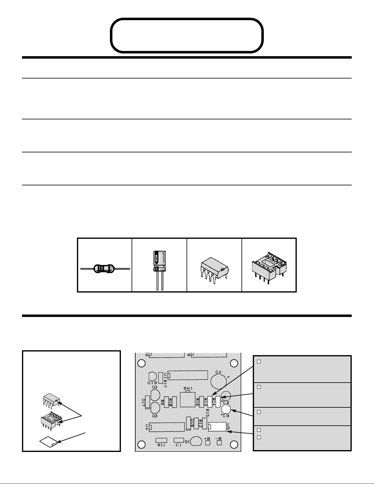
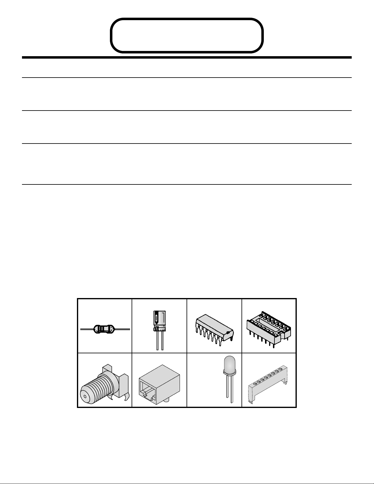
PARTS LIST - SECTION A
RESISTORS
Qty. Symbol Description Color Code Part #
! 2 R12, R17 1kΩ 5% 1/4W brown-black-red-gold 141000
! 1 R16 5.6kΩ 5% 1/4W green-blue-red-gold 145600
! 1 R15 12kΩ 5% 1/4W brown-red-orange-gold 151200
! 1 R9 3.3MΩ 5% 1/4W orange-orange-green-gold 173300
CAPACITORS
Qty. Symbol Value Description Part #
! 1 C2 22µF Electrolytic Radial 272244
SEMICONDUCTORS
Qty. Symbol Value Description Part #
! 1 D17 1N4001 Silicon Diode 314001
! 1* 1N4736 Zener Diode 6.8V 1W 314736
! 1 D18 1N5235 Zener Diode 6.8V 0.5W 315235
! 2 Q2, Q3 2N3904 Transistor NPN 323904
! 1 Q1 2N3906 Transistor PNP 323906
! 1 D19 LED Red 350003
! 1 U4 40106 Integrated Circuit (IC) Hex Inverter 330106
MISCELLANEOUS
Qty. Symbol Description Part #
! 1 PC Board Tester TCT-200 517041
! 1 SW1 Switch Push Button DPDT 540203
! 1 Battery 9V 590009
! 1 Battery Snap 9V 590098
! 1 Spacer 624018
! 1 U4 Socket IC 14-pin 664014
! 1 Tubing #20 1/2” 890020
! 1 Solder Tube, Lead-free 9LF99
* Packaged in a separate bag, used for testing only.
SECTION A
Power Supply
PARTS IDENTIFICATION
Integrated Circuit (IC)
-5-
Resistor DiodesElectrolytic Transistor LED
IC Socket 14-pin
PC Board (Tester)
Switch Push Button
Epoxy
Zener
Battery Snap
Spacer
Tubi ng
Page 7

Figure B
Mount the LED with the tubing and
plastic spacer to the PC board as
shown. Note the flat side of the
LED and the PC board marking.
ASSEMBLE THE FOLLOWING COMPONENTS TO THE PC BOARD
In all of the following steps the components must be installed on the top legend side of the PC board. The
board is turned to solder the component leads on the foil side.
R17 - 1kΩ 5% 1/4W Resistor
(brown-black-red-gold)
(see Figure A)
D19 - LED Red
Tubing
Spacer
(see Figure B)
R9 - 3.3MΩ 5% 1/4W Resistor
(orange-orange-green-gold)
(see Figure A)
Q2 - 2N3904 Transistor NPN
(see Figure C)
D17 - 1N4001 Diode (epoxy)
(see Figure D)
Q3 - 2N3904 Transistor NPN
(see Figure C)
U4 - 14-pin IC Socket
U4 - 40106 IC Hex Inverter
(see Figure E)
SW1 - Push Button Switch
(see Figure F)
R16 - 5.6kΩ 5% 1/4W Resistor
(green-blue-red-gold)
(see Figure A)
C2 - 22µF Electrolytic
(see Figure G)
R15 - 12kΩ 5% 1/4W Resistor
(brown-red-orange-gold)
(see Figure A)
R12 - 1kΩ 5% 1/4W Resistor
(brown-black-red-gold)
(see Figure A)
D18 - 1N5235 Zener Diode 0.5W
(see Figure D)
Battery Snap
(see Figure H)
Q1 - 2N3906 Transistor PNP
(see Figure C)
Figure A
Mount the resistor
flat against the PC
board as shown.
Figure D
Diodes have polarity. Mount the
diodes in the direction marked on
the PC board as shown.
Polarity
Marking
Polarity
Marking
Epoxy
Zener
-6-
Figure F
IMPORTANT!!! Mount the push button
switch as shown. The circle MUST be
facing the other direction from the marking
“SW1” on the PC board.
Figure G
Electrolytic capacitors have polarity. Be sure
to mount them with the negative (–) lead
(marked on the side) in the correct hole.
Flat Side
Spacer
LED
Tubing
Figure C
Mount the
transistor to
the PC board
noting the flat
side.
Flat Side
Figure E
Insert the IC socket into the PC board with the
notch in the direction shown on the top
legend. Solder the IC socket into place.
Insert the IC into the socket with the notch in
the same direction as the notch on the socket.
Notch
Notch
Marking
Figure H
Mount the battery
snap as shown.
The black (–) lead
goes to –B and
the red (+) lead
goes to +B.
Circle
Red Lead
Black Lead
(–) (+)
1/8”
Warning:
If the capacitor is connected
with incorrect polarity, it may
heat up and either leak, or
cause the capacitor to
explode.
Polarity Marking
Page 8

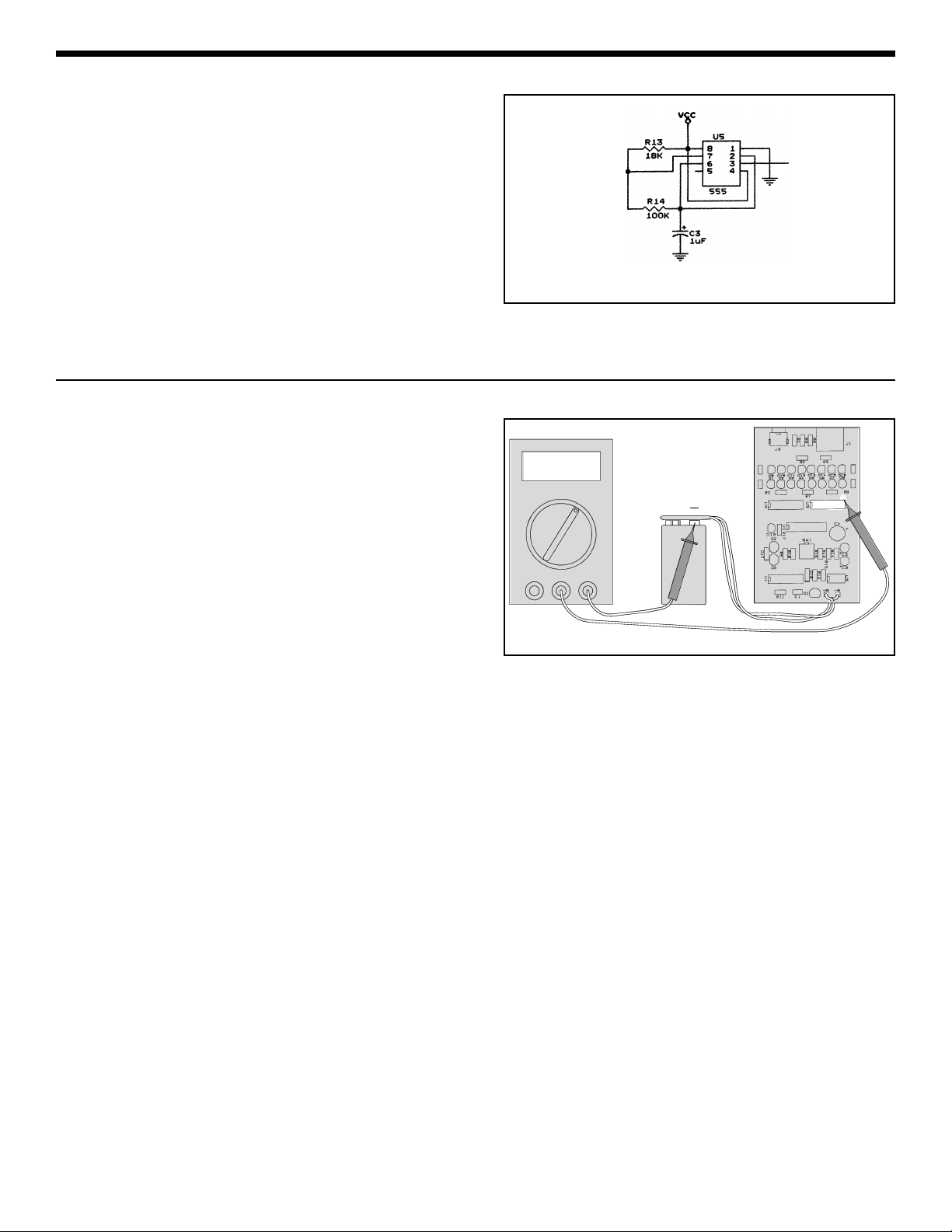
SECTION A - POWER SUPPLY
When the SW1 (test button) is pushed, capacitor C2
(see schematic diagram, Figure 1) is charged to the
battery voltage. Transistor Q1 turns on and all of the
circuits in the tester are powered. If you don’t push
SW1, capacitor C2 begins discharging. When the
voltage on C2 is less than 0.7V, transistor Q1 and
the power turn off after 30-50 seconds.
When the voltage of the battery is less than 7.5V,
transistors Q2 and Q3 turn on and LED D19 (Low
Battery) lights. The diode D17 protects the tester
from wrong polarity input voltage.
-7-
! 1. Connect the battery to the battery snap.
! 2. Set the voltmeter to read 20VDC and connect
the COM lead to the negative (–) side of the
battery and the V lead to the positive (+) side
of the battery as shown in Figure 2. The meter
should indicate 9-10VDC. Push switch SW1.
! 3. Remove the V lead from the positive (+) side
of the battery and move to pad of pin 4 of IC
U5. The meter should indicate the same
voltage, but after 30-50 seconds, the voltage
should drop to 0V.
! 4. Push the switch SW1 again. The meter should
indicate the same voltage as in step 2. If not:
a) Check that the battery snap is connected
with the the right polarity as shown in the
assembly instructions.
b) Check that the transistor Q1 is 2N3906
and mounted with the emitter, base and
collector leads as shown in the assembly
instructions.
c) Check that R9, R12 and C2 are the
correct values.
d) Check that D17, D18, C2, U4 and SW1
are installed as shown in the assembly
instructions.
! 5.
Bend the zener diode 1N4736 (6.8V 1W,
located in a separate bag) as shown in Figure 3.
P
ush the switch SW1 again and short the
battery by the zener diode for 1-2 seconds (the
side with the band should be touching the “+”
terminal of the battery, see Figure 2). LED D19
(Lo Batt.) should be lit. Remove the zener diode
and the LED should turn off. If not:
a) Check that the transistors Q2 and Q3
are 2N3904 and mounted as shown in
the assembly instructions.
b) Check zener diode D18 and LED D19.
Be sure that they are installed as shown
in the assembly instructions.
c) Check that resistors R15, R16 and R17
are the correct values.
Remove the battery from the battery snap and
the leads from the tester.
TESTING
Figure 1
Figure 3
0.5” - 0.6”
V
COM
VDC
+
9V
Figure 2
1
8
Page 9
PARTS LIST - SECTION B
RESISTORS
Qty. Symbol Description Color Code Part #
! 1 R13 18kΩ 5% 1/4W brown-gray-orange-gold 151800
! 1 R14 100kΩ 5% 1/4W brown-black-yellow-gold 161000
CAPACITORS
Qty. Symbol Value Description Part #
! 1 C3 1µF Electrolytic Radial 261047
SEMICONDUCTORS
Qty. Symbol Value Description Part #
! 1 U5 555 Integrated Circuit (IC) 555 Timer 330555
MISCELLANEOUS
Qty. Symbol Description Part #
! 1 U5 Socket IC 8-pin 664008
SECTION B
Oscillator
PARTS IDENTIFICATION
-8-
Resistor
Integrated Circuit (IC)
Electrolytic IC Socket 8-pin
Figure I
Insert the IC socket into the PC board with the
notch in the direction shown on the top
legend. Solder the IC socket into place.
Insert the IC into the socket with the notch in
the same direction as the notch on the socket.
ASSEMBLE THE FOLLOWING COMPONENTS TO THE PC BOARD
In all of the following steps the components must be installed on the top legend side of the PC board. The
board is turned to solder the component leads on the foil side.
R13 - 18kΩ 5% 1/4W Resistor
(brown-gray-orange-gold)
(see Figure A)
R14 - 100kΩ 5% 1/4W Resistor
(brown-black-yellow-gold)
(see Figure A)
C3 - 1µF Electrolytic Radial
(see Figure G)
U5 - 8-pin IC Socket
U5 - 555 IC Timer
(see Figure I)
Notch
Notch
Marking
Page 10
! 1. Connect the battery to the battery snap.
! 2. Set the voltmeter to read 20VAC and connect
the COM lead to the negative (–) side of the
battery and the V lead to pad of pin 8 of IC U3
as shown in Figure 5. The meter should
indicate 0V. Push switch SW1. The meter
should indicate 3-5VAC.
If not:
a) Check U5 and C3 to be sure that they
are installed as shown in the assembly
instructions.
b) Check R13 and R14 are the correct
values.
Remove the battery from the battery snap and
the leads from the tester.
-9-
SECTION B - OSCILLATOR
The oscillator section consists of a 555 timing
circuit, resistors R13, R14, and capacitor C3. The
555 IC is configured as an astable or free-running
oscillator. The values of the resistor R14 and
capacitor C3 set the output frequency at 8Hz. The
IC will produce a continuous 8Hz square wave from
pin 3 as long as it is powered.
TESTING
Figure 4
To Switches
Figure 5
V
COM
VAC
+
9V
1
14
Page 11
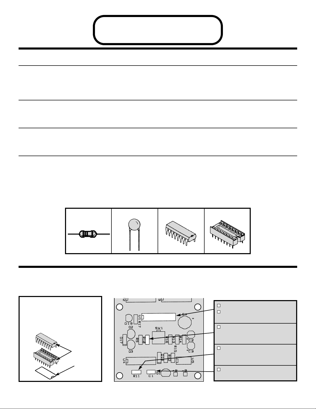
Figure J
Insert the IC socket into the PC board with the
notch in the direction shown on the top
legend. Solder the IC socket into place.
Insert the IC into the socket with the notch in
the same direction as the notch on the socket.
-10-
PARTS LIST - SECTION C
RESISTORS
Qty. Symbol Description Color Code Part #
! 1 R11 680kΩ 5% 1/4W blue-gray-yellow-gold 166800
! 1 R10 1.2MΩ 5% 1/4W brown-red-green-gold 171200
CAPACITORS
Qty. Symbol Value Description Part #
! 1 C1 .001µF Discap (102 or .001) 231035
SEMICONDUCTORS
Qty. Symbol Value Description Part #
! 1 U1 4017 Integrated Circuit (IC) Decade Counter 334017
MISCELLANEOUS
Qty. Symbol Description Part #
! 1 U1 Socket IC 16-pin 664016
SECTION C
Step Pulses with Counter
PARTS IDENTIFICATION
Resistor
Integrated Circuit (IC)
Capacitor
IC Socket 16-pin
102
ASSEMBLE THE FOLLOWING COMPONENTS TO THE PC BOARD
In all of the following steps the components must be installed on the top legend side of the PC board. The
board is turned to solder the component leads on the foil side.
U1 - 16-pin IC Socket
U1 - 4017 IC Decade Counter
(see Figure J)
R10 - 1.2MΩ 5% 1/4W Resistor
(brown-red-green-gold)
(see Figure A)
R11 - 680kΩ 5% 1/4W Resistor
(blue-gray-yellow-gold)
(see Figure A)
C1 - .001µF Discap
(102 or .001)
Notch
Notch
Marking
Page 12
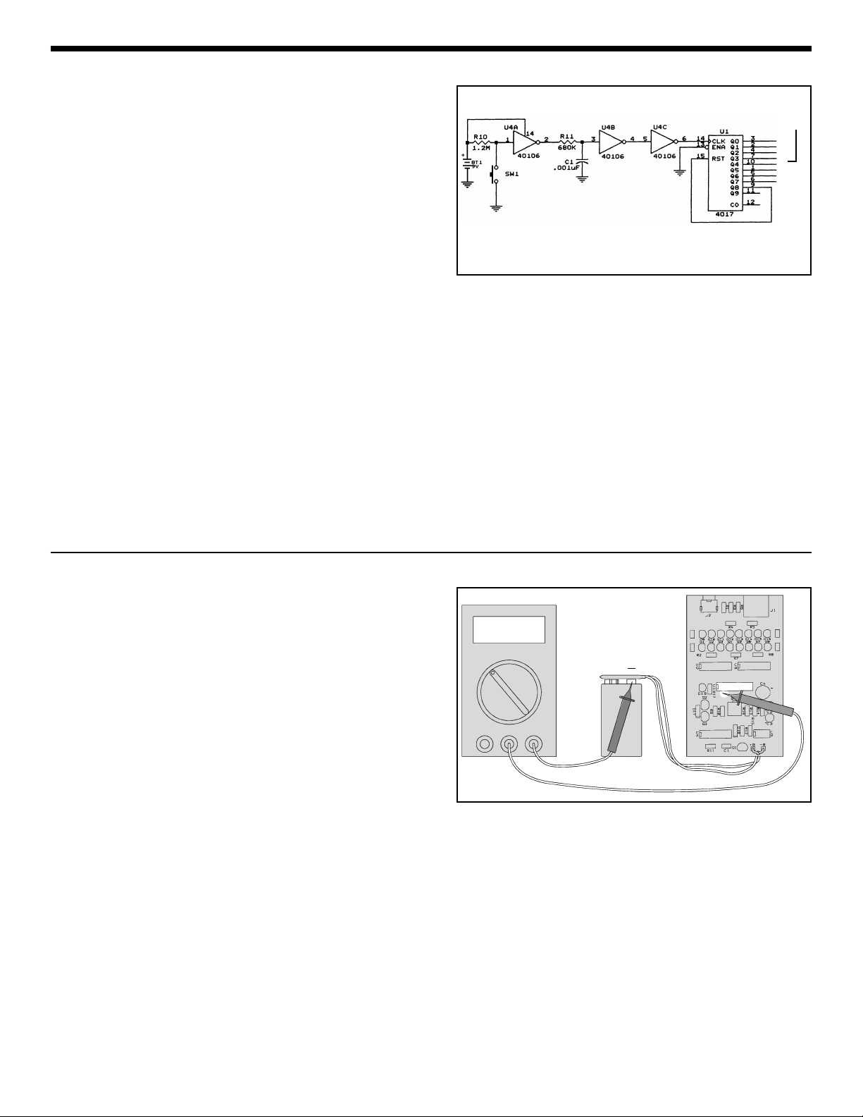
! 1. Connect the battery to the battery snap.
! 2. Set the voltmeter to read 20VDC and connect
the COM lead to the negative (–) side of the
battery and the V lead to pin 3 of IC U1 as
shown in Figure 7.
! 3.
Push switch SW1 until the voltmeter
indicates 9-10VDC.
! 4. Move the V lead of the voltmeter to pin 2. The
voltmeter should indicate 0V. Push SW1
again. The voltmeter should indicate 8-9VDC.
In the same manner, test the outputs of the
counter (pins 4, 7, 10, 1, 5, and 6).
If the test results are not satisfactory, then:
a) Check U1. Be sure that it is installed as
shown in the assembly instructions.
Remove the battery from the battery snap and
the leads from the tester.
SECTION C - STEP PULSES WITH COUNTER
In this section, a 4017 counter IC and a 40106
inverter IC are used to control eight electronic
switches. A short positive pulse must be generated
and applied to the clock input of the 4017 IC
whenever switch SW1 is depressed. This is done by
wiring three inverters in series. When switch SW1 is
depressed, the voltage at pin 1 of the 40106 is
pulled to ground. This low condition is then inverted
three times to produce a positive pulse to the CLK
pin of the 4017.
The 4017 IC is a five-stage Johnson decade
counter. The IC has 10 outputs, but only one output
will be driven high at any given time, the other nine
will be low. For each pulse at the clock (CLK) input,
the output will move one position. In this design,
only eight outputs are used, the ninth output is wired
to the reset (RST) pin. When the reset pin goes
high, it sets the Q0 output high again. The clock
enable (ENA) pin is tied to ground, so every clock
pulse will move the output.
TESTING
Figure 6
-11-
To Switches
}
1
16
VDC
9V
+
V
COM
Figure 7
Page 13
-12-
PARTS LIST - SECTION D
RESISTORS
Qty. Symbol Description Color Code Part #
! 8 R1-R8 200Ω 5% 1/4W red-black-brown-gold 132000
CAPACITORS
Qty. Symbol Value Description Part #
! 1 C4 470µF 16V Electrolytic Radial 284744
SEMICONDUCTORS
Qty. Symbol Value Description Part #
! 16 D1-D16 LED Red 350003
! 2 U2, U3 74HC4066 Integrated Circuit (IC) Quad Analog Switch 394066
MISCELLANEOUS
Qty. Symbol Description Part #
! 1 J2 F-Connector 590500
! 1 J1 Modular Jack RJ-45 621028
! 2 Spacer 624006
! 2 U2, U3 IC Socket 14-pin 664014
SECTION D
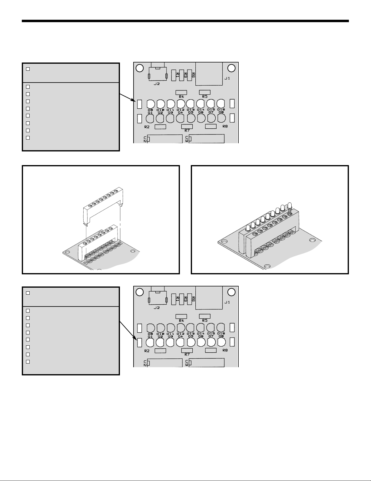
Switches and LED Indicator
PARTS IDENTIFICATION
Resistor
Integrated Circuit (IC)
Electrolytic IC Socket 14-pin
F-Connector Modular Jack LED
Spacer
Page 14

ASSEMBLE THE FOLLOWING COMPONENTS TO THE PC BOARD
In all of the following steps the components must be installed on the top legend side of the PC board. The
board is turned to solder the component leads on the foil side.
R6 - 200Ω 5% 1/4W Resistor
(red-black-brown-gold)
(see Figure A)
R3 - 200Ω 5% 1/4W Resistor
(red-black-brown-gold)
(see Figure A)
R1 - 200Ω 5% 1/4W Resistor
(red-black-brown-gold)
(see Figure A)
J2 - F-Connector
(see Figure K)
R4 - 200Ω 5% 1/4W Resistor
(red-black-brown-gold)
(see Figure A)
R2 - 200Ω 5% 1/4W Resistor
(red-black-brown-gold)
(see Figure A)
R7 - 200Ω 5% 1/4W Resistor
(red-black-brown-gold)
(see Figure A)
U2 - 14-pin IC Socket
U2 - 74HC4066 IC
(see Figure E)
J1 - Modular Jack RJ-45
(see Figure L)
R5 - 200Ω 5% 1/4W Resistor
(red-black-brown-gold)
(see Figure A)
R8 - 200Ω 5% 1/4W Resistor
(red-black-brown-gold)
(see Figure A)
U3 - 14-pin IC Socket
U3 - 74HC4066 IC
(see Figure E)
C4 - 470µF Electrolytic Radial
(see Figure G)
-13-
Figure K
Mount and solder the F-connector to the PC board in the
location shown. Note: The connector must be
soldered in straight.
Figure L
Mount and solder the modular jack to the PC board as
shown.
Page 15
-14-
ASSEMBLE THE FOLLOWING COMPONENTS TO THE PC BOARD (cont.)
Spacer
(see Figure M)
D9 - LED
D10 - LED
D11 - LED
D12 - LED
D13 - LED
D14 - LED
D15 - LED
D16 - LED
(see Figure N)
Figure M
Mount the spacer to the PC board as shown.
Figure N
Mount the LEDs onto the spacer as shown. Note the flat
side of the LED in relation to the marking on the PC
board. Solder and cut off the excess leads.
Spacer
(see Figure M)
D1 - LED
D2 - LED
D3 - LED
D4 - LED
D5 - LED
D6 - LED
D7 - LED
D8 - LED
(see Figure N)
Page 16

! 1. Connect the battery to the battery snap.
! 2. Push the switch SW1. Two vertical LEDs
should be blinking at a frequency of
approximately 8Hz.
! 3. Test the other pairs of LEDs by pushing switch
SW1. For every step, there should be only two
vertical blinking LEDs. If not, then:
a) Check U2, U3, C4 and diodes D1-D16.
Be sure that they are installed as shown
in the assembly instructions.
b) Check that the resistors R1-R8 installed
are the correct values.
c) Check the soldering on the modular jack
and F-connector.
TESTING
Figure 10
SECTION D - SWITCHES AND LED INDICATOR
In this section, two quad analog switches
(74HC4066) and 16 LEDs are used to indicate
which pins are being tested and the type of cable.
Figure 8 shows the logic diagram for each switch.
Each switch contains an input, output and a control
pin. The inputs are connected to the oscillator
section and the outputs to two LEDs and connector.
The control pins connect to the outputs of the 4017
IC (see Figure 10).
When switch A is closed, capacitor C charges and
discharges at the oscillator frequency. This causes
LEDs D1 and D2 to blink at the same rate (see
Figure 9a).
Connecting a straight cable, LED D3 will light only
during the charging cycle. The diode in the
terminator only allows the current flow in one
direction (see Figure 9b).
Connecting a cross-pinning cable, LED D4 will light
only during the discharging cycle (see Figure 9c).
Figure 8
Without Terminator
Figure 9a
ON/OFF Control
Analog
Input/Output
Analog
Output/Input
-15-
{
From
Counter
From Oscillator
Charge
Discharge
Straight Cable
Figure 9b
Cross-Pinning Cable
Figure 9c
A
B
A
B
A
B
Page 17

-16-
PARTS LIST - SECTION E
SEMICONDUCTORS
Qty Symbol Value Description Part #
! 4 D1-D4 1N4148 Diode 314148
MISCELLANEOUS
Qty Symbol Description Part #
! 1 PC Board Terminator LD-100 510005
! 1 J2 F-Connector 590500
! 1 J1 Modular Jack RJ-45 621028
SECTION E
Terminato r
PARTS IDENTIFICATION
F-Connector Modular Jack Diode PC Board
ASSEMBLE THE FOLLOWING COMPONENTS TO THE PC BOARD
In all of the following steps the components must be installed on the top legend side of the PC board. The
board is turned to solder the component leads on the foil side.
D4 - 1N4148 Diode
D3 - 1N4148 Diode
D2 - 1N4148 Diode
D1 - 1N4148 Diode
(see Figure D)
Note: R1 is not used.
Modular Jack (RJ-45)
(see Figure L)
J2 - F-Connector
Note: The connector must be
soldered in straight.
(see Figure K)
IMPORTANT: Cut off the excess
leads after soldering the FConnector to the PC board.
Page 18
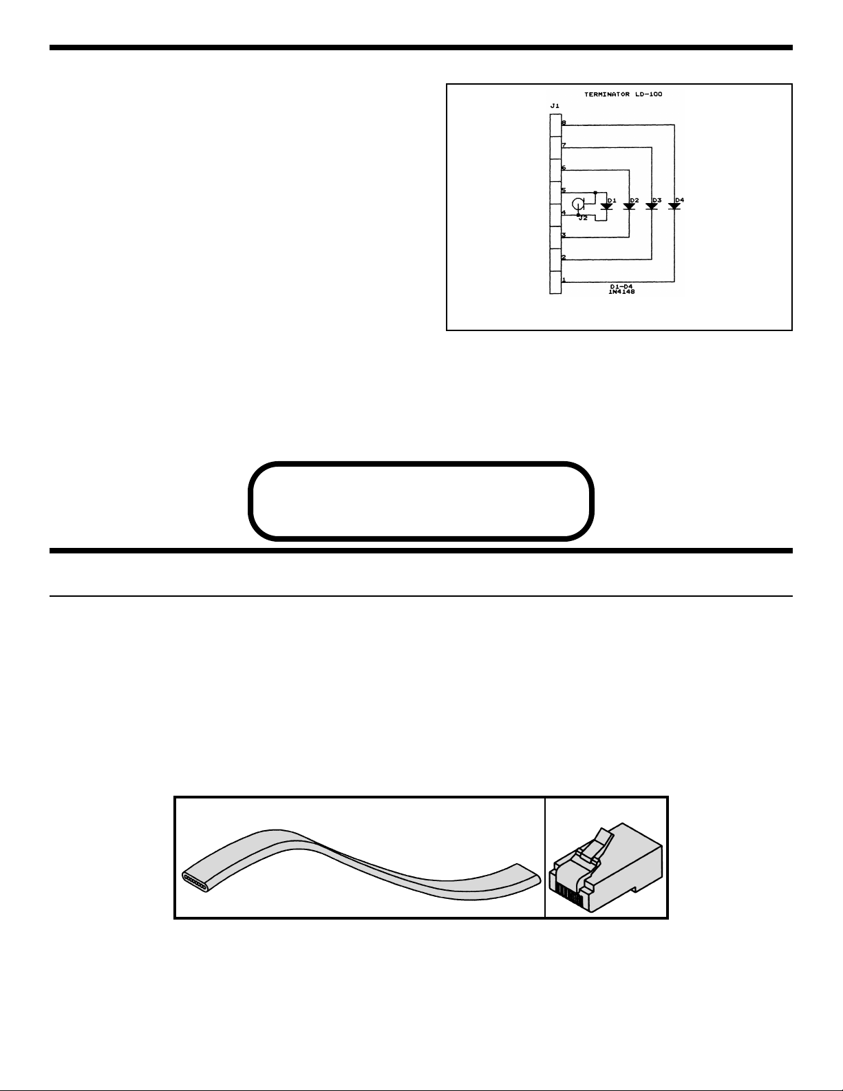
SECTION E - TERMINATOR
The terminator uses four diodes to identify the
polarity of the input signals. The diodes are placed
in series with wires 1-8, 2-7, 3-6, and 4-5 (see
Figure 11).
Figure 11
PARTS LIST - SECTION F
MISCELLANEOUS
Qty. Symbol Description Part #
! 4 Plug RJ-45 621032
! 2’ Cable Flat 8 Wires 870984
SECTION F
Assemble Telecom Cables
PARTS IDENTIFICATION
Plug RJ-45
8 Wire Flat Cable
-17-
Page 19

-18-
ASSEMBLE THE TELECOM CABLES
For testing and troubleshooting the tester, you need to assemble straight and cross-pinning cables.
For cutting, stripping, and crimping, use a standard tool for RJ-45 plugs (flat cable).
ELENCO®has modular crimping tools Models ST-500 and HT-568.
! Cut the 2’ telecom cable in half (see Figure 12).
! Using the instructions for your tool, make two
cables (straight and cross-pinning) as shown in
Figures 13 - 15. Make sure that you make a
clean cut on the cable.
Figure 12 Cutting Figure 13 Stripping
Figure 15 Crimping
Figure 14
(BL) 1
(OR)2
(BK) 3
(R) 4
(G) 5
(Y) 6
(BN) 7
(S) 8
1
2
3
4
5
6
7
8
(BL) 1
(OR)2
(BK) 3
(R) 4
(G) 5
(Y) 6
(BN) 7
(S) 8
1
2
3
4
5
6
7
8
Straight Cable
Cross-Pinning Cable
Note the orientation of the
RJ-45 plug for each cable.
Page 20

-19-
PARTS LIST - SECTION G
MISCELLANEOUS
Qty. Symbol Description Part #
! 2 F to BNC Adapter 596020
! 1 Button Cap 622006
! 1 Case Top Tester 623114
! 1* Case Top Terminator 623115
! 1 Case Bottom Tester 623211
! 1* Case Bottom Terminator 623212
! 1 Cover Battery 623401
! 1 Velcro Hook and Loop Set 628002
! 2 Screw 2.6 x 8mm Thread Cutting Phillips Pan Head 642109
! 4 Screw 3 x 12mm Thread Cutting Phillips Flat Head 643104
! 1 Screw M3 x 10mm Machine Phillips Flat Head 643105
! 1* Screw 2.6 x 10mm Thread Cutting Phillips Flat Head 643107
! 1* Label Terminator 727050
! 1 Label Tester 727051
* Used for the assembly of the terminator.
SECTION G
Final Test and Assembly
PARTS IDENTIFICATION
Button Cap Case Top Terminator
Case Top Tester Case Bottom Tester
Case Bottom Terminator Cover Battery
Velcro Hook & Loop Set Screws (actual size) Label Tester Label Terminator
2.6 x 8mm Thread
Cutting Phillips Pan Head
3 x 12mm Thread Cutting
Phillips Flat Head
2.6 x 10mm Thread
Cutting Phillips Flat Head
Hook
Loop
F to BNC
Adapter
M3 x 10mm Machine
Phillips Flat Head
Page 21

Straight Cable
! 1.
Connect one end of the straight cable to the
modular jack on the PC board of the terminator
and the second end to the PC board of the
cable tester as shown in Figure 16a.
! 2. Push switch SW1 until the two vertical LEDs
D1 and D9 are blinking alternately and LED
D16 should be blinking too.
! 3.
Check the other LEDs by pressing switch SW1
and referring to Table 1 below. The single
blinking LED should always be on the top row.
If the LEDs are not functioning properly, then:
a) Check the cable using a master tester.
b) Check the ICs U2, U3 and LEDs D1-D16
on the PC board of the tester. They
should be mounted as shown in the
assembly instructions.
c)
Check that resistors R1-R8 on the PC board
of the tester are the correct values (200Ω).
d) Check diodes D1-D4 on the PC board of
the terminator. Be sure that the diodes
are installed as shown in Figure D in the
assembly instructions.
Cross-Pinning Cable
! 1. Remove the straight cable and connect the
cross-pinning cable to the modular jacks on
the PC boards of the tester and terminator.
! 2. Push switch SW1 until the two vertical LEDs
D1 and D9 are blinking alternately and LED
D8 should be blinking too.
! 3.
Check the other LEDs by pressing switch SW1
and referring to Table 2 below. The single LED
should always be on the bottom row. If not, then:
a) Check the cable using the master tester.
b) Check diodes D1-D4 on the PC board of
the terminator. Be sure that the diodes
are installed as shown in Figure D in the
assembly instructions.
Short Test
! 1. Push switch SW1 until the two vertical LEDs
D4 and D12 are blinking alternately and LED
D5 is blinking too.
! 2.
Using a short piece of wire or a discarded lead from
one of the components, short the F-connector on
the terminator PC board as shown in Figure 16b.
The LED D13 should be blinking too. Remove the
jumper and LED D13 should turn off. If not, then:
a) Check the F-connector on the terminator PCB.
!3.Short the F-connector on the tester PC board. The
LED D13 should be blinking again. If not, then:
a) Check the F-connector on the terminator PCB.
! 4. Remove the cable from the modular jacks on
the PC board and proceed to the final
assembly.
-20-
SECTION G - FINAL TEST
Two Ver t ical Straight Cable
# Blinking LEDs Single Blinking
LED on Top Row
1 D1 and D9 D16
2 D2 and D10 D15
3 D3 and D11 D14
4 D4 and D12 D13
5 D5 and D13 D12
6 D6 and D14 D11
7 D7 and D15 D10
8 D8 and D16 D9
Figure 16b
Figure 16a
Two Ver t ical Cross-Pinning Cable
# Blinking LEDs Single Blinking
LED on Bottom Row
1 D1 and D9 D8
2 D2 and D10 D7
3 D3 and D11 D6
4 D4 and D12 D5
5 D5 and D13 D4
6 D6 and D14 D3
7 D7 and D15 D2
8 D8 and D16 D1
Table 1
Table 2
Page 22

-21-
SECTION G - FINAL ASSEMBLY OF TESTER
!
Push the button cap onto the switch as shown in Figure O.
! Mount the PC board to the top case, as shown in
Figure P, with two 2.6 x 8mm phillips screws.
Note: The button cap should be centered in the
top case hole. Make sure that the Lo Batt LED
goes through the hole in the case.
! Wrap the wires from the battery snap around the
battery housing as shown in Figure Q.
! Mount the bottom case to the front case, as
shown in Figure Q, using four 3 x 12mm flat
phillips screws. Be sure that the battery snap is
through the battery compartment hole as shown.
! Connect the 9V battery to the battery snap and
place it into the case. Slide the battery cover onto
the case as shown in Figure R.
Figure O
Figure P Figure R
2.6 x 8mm Screws
PC Board
Top Case
Battery Cover
9V Battery
Button Cap
Bottom Case
3 x 12mm Screws
Figure Q
Page 23

-22-
M3 Phillips
Screw
! Insert the M3 x 10mm machine phillips screw into
the battery cover hole, as shown in Figure S, and
tighten.
! Peel the backing off of the label and stick it onto
the front case as shown in Figure T. Use the hole
in the middle to line up the label. Note: Be very
careful when applying this label. The adhesive is
very sticky and when the label is on, it’s on!
Figure S
Figure U
Figure T
FINAL ASSEMBLY OF TESTER (cont.)
! Before assembling, check that the excess leads
from the F-connector are cut off (see page 16).
! Assemble the terminator as shown in Figure U.
Insert the 2.6 x 10mm flat phillips screw and
tighten down.
!
Peel the backing off of the terminator label and
carefully place it onto the unit as shown in Figure V.
Note: Be sure that the terminator has been
tested and is in working order before you apply
the label.
FINAL ASSEMBLY OF TERMINATOR
2.6 x 10mm Flat
Phillips Screw
Top Load Case
Load PC Board
Bottom Load Case
Label
Figure V
Load Label
Page 24

-23-
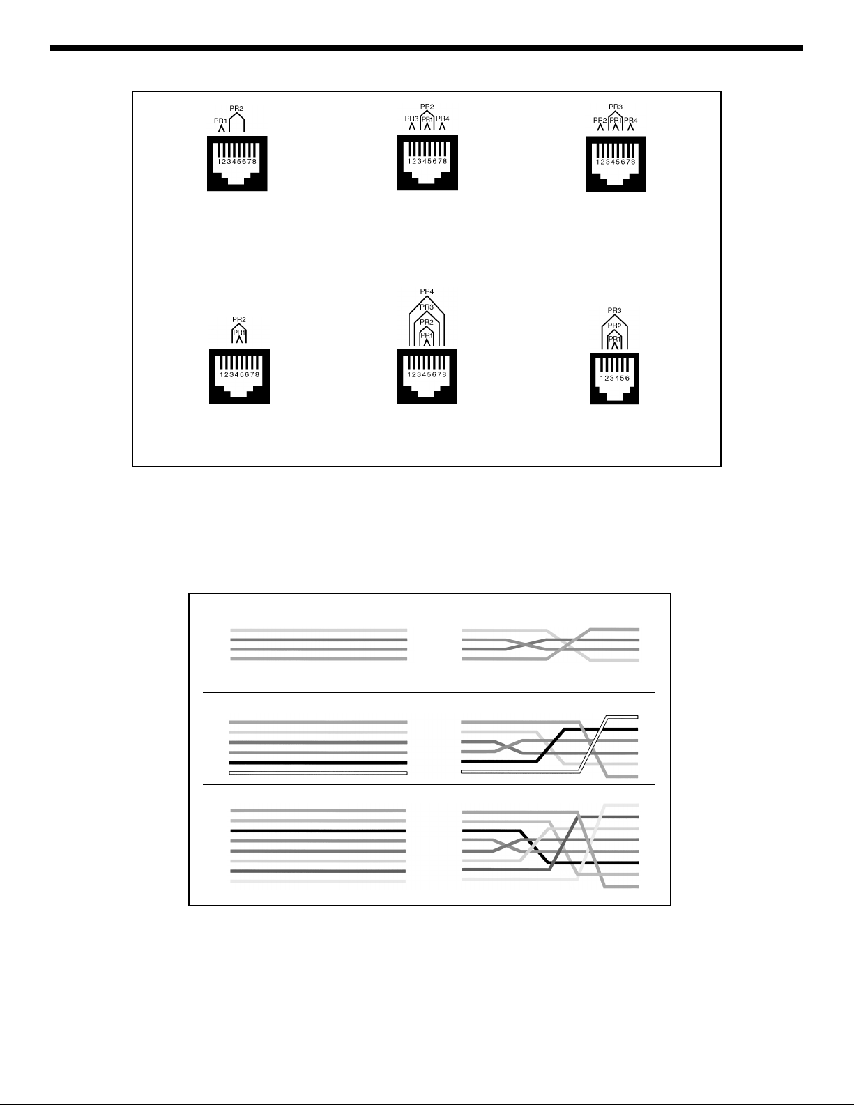
CATEGORY OF CABLE
• Unshielded communication cable with RJ-11 and
RJ-45 connectors.
• Ethernet 10 Base-T, Token Ring, EIA/TIA-568A/B,
AT&T 258A, and USOC.
• 50 or 75Ω coaxial cable with F connectors.
• 50 or 75Ω coaxial cable with BNC connectors.
Must use F to BNC adapters.
Maximum testing length for all cable types is
1,000 feet.
MULTIPLE FUNCTIONS
• Testing cables before or after their installation.
• Mapping Function (to test individual wire pairs or
coaxial cables).
• Cable identification (straight or cross-pinning).
• Pair identification (straight or cross-pinning).
• Open/short wiring test.
ENVIRONMENTAL CONDITIONS
• Operating Conditions: 0OC - 45OC / 32OF - 113OF
70% RH max.
• Storage Conditions: -10OC - 50OC / 14OF - 122OF
80% RH max.
POWER
• Standard or alkaline 9V battery
• Low battery indicator (Lo Batt.)
• Auto power-off function (30 s)
SPECIFICATIONS
! Peel off the two backings, and attach the two
velcro pieces onto the terminator and the tester
in the location shown in Figure W.
FINAL ASSEMBLY (cont.)
Figure W
Velcro Pieces
Page 25

-24-
Configuration
for Testing
Communication
Cable
Configuration
for Testing
Coaxial Cable
1. Connect one end of the cable to be tested to the
terminator and the other end to the cable tester
as shown in Figure 17.
2.
Push the TEST (power) button and read the result.
Good Pair: Two vertical and one single blinking
LEDs. The location of the single LED indicates a
straight or cross-pinning for the pair.
Open Pair: Only two vertical LEDs blinking.
Short: Four or more LEDs are blinking (two or
more wires are shorted).
3. Push the TEST button again and read the result
for the next pair.
4.
For testing coax cable, use the middle LEDs (boxed
in as coax on the unit).
5.
If you do not push the button for 30 seconds, it will
automatically shut off.
CAUTION
DO NOT test cable connected to electric power. To avoid electric
shock, disconnect the power to the cable under test. Connection to
an active power cable can result in injury or even death.
*
*
*
*
*
*
*
*
*
Open Pair
For straight open wire #3
For Cross-Pinning
open wire #6
Short
Cross-Pinned cable
short wires 6 & 7
*
= Blinking LED
*
*
*
Good Pair (Cross-Pinning)
3 & 6 Wires
Good Pair (Straight)
3 & 6 Wires
OPERATION INSTRUCTIONS
Figure 17
Page 26
-25-
Ethernet
10Base-T
EIA/TIA-568A EIA/TIA-568B
AT&T 258A
8-Position
Token Ring
USOC USOC
(Prs. 1,2 & 3)
(Y) 1
(G) 2
(R) 3
(BL) 4
(Y) 1
(G) 2
(R) 3
(BL) 4
1
2
3
4
(BL) 1
(Y) 2
(G) 3
(R) 4
(BK) 5
(W) 6
1
2
3
4
5
6
(BL) 1
(Y) 2
(G) 3
(R) 4
(BK) 5
(W) 6
1
2
3
4
5
6
(BL) 1
(OR)2
(BK) 3
(R) 4
(G) 5
(Y) 6
(BN) 7
(S) 8
1
2
3
4
5
6
7
8
(BL) 1
(OR)2
(BK) 3
(R) 4
(G) 5
(Y) 6
(BN) 7
(S) 8
1
2
3
4
5
6
7
8
RJ-11 (4-Wire) Straight-Pinning RJ-11 (4-Wire) Cross-Pinning
RJ-11 (6-Wire) Straight-Pinning
RJ-11 (6-Wire) Cross-Pinning
RJ-45 (8-Wire) Straight-Pinning RJ-45 (8-Wire) Cross-Pinning
NOTE: Cross-Pinning is for typical telephone use.
WIRING SCHEMES
1
2
3
4
Page 27
-26-
GENERAL MAINTENANCE
To clean, wipe the case with a damp cloth and
detergent (do not use abrasives or solvents).
When the Lo Batt. LED lights up, you need to
replace the battery. The terminator does not use
a battery.
BATTERY REPLACEMENT
The tester is powered by a single standard or
alkaline 9V battery. Use the following procedure to
replace the battery.
1. Disconnect the cables from the tester.
2. Using a phillips screwdriver, remove the battery
cover screw and open the battery cover.
3. Carefully remove the old battery and replace with
a new battery.
4. Reinsert the battery into the case, dressing the
battery leads so that they will not be pinched
between the case and the battery cover.
5. Reinstall the battery cover and screw.
MAINTENANCE
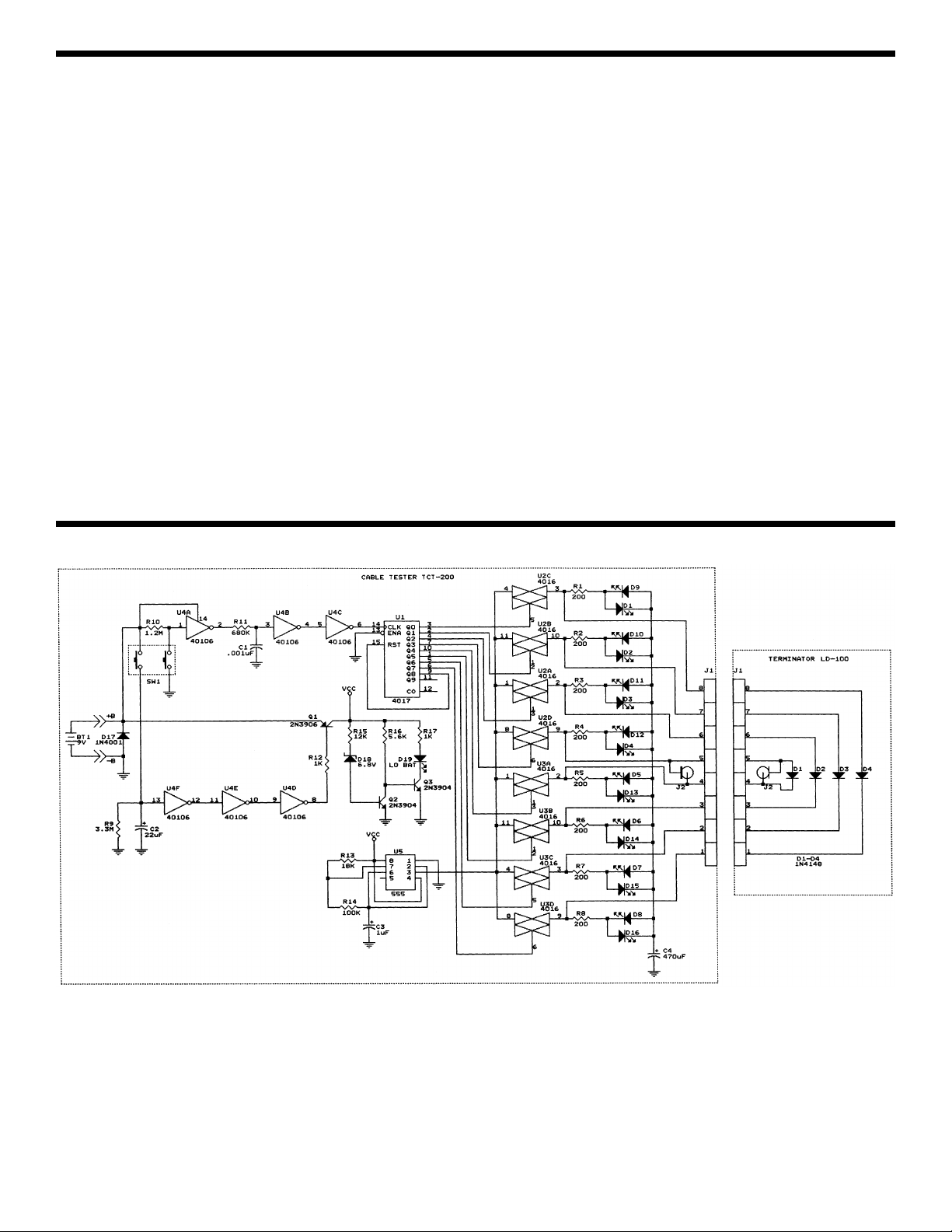
SCHEMATIC DIAGRAM
Page 28

ELENCO
®
150 Carpenter Avenue
Wheeling, IL 60090
(847) 541-3800
www.elenco.com
email: elenco@elenco.com
 Loading...