

Page 1
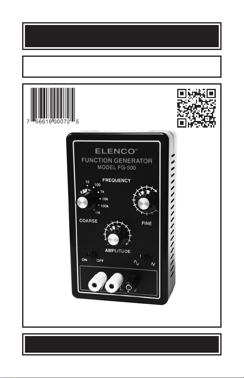
Function Generator
MODEL FG-500
Instruction Manual
ELENCO
®
Copyright © 2012, 2003 Elenco®Electronics, Inc. REV-D 753068
Page 2

SPECIFICATIONS
OUTPUT:
• Waveforms: Sine, triangle, square
• Impedance: 600Ω ±10%
• Frequency: 1Hz - 1MHz in 6 decade steps with variable ranges.
SINE WAVE:
• Amplitude: 0 - 3Vpp
• Distortion: Less than 1% (at 1kHz)
• Flatness: ±0.05dB 1Hz - 100kHz
SQUARE WAVE:
• Amplitude: 8V (no load)
• Rise Time: Less than 50ns (at 1kHz)
• Fall Time: Less than 30ns (at 1kHz)
• Symmetry: Less than 5% (at 1kHz)
TRIANGLE WAVE:
• Amplitude: 0 - 3Vpp
• Linearity: Less than 1% (up to 100kHz)
POWER REQUIREMENTS:
• Standard 9V battery
OPERATING TEMPERATURE:
• 32OF (0OC) to 122OF (50OC)
-1-
Page 3

-2-
INTRODUCTION
Your FG-500 Function Generator contains a complete function generator capable
of producing sine, square and triangle wave forms. The frequency of this generator
can be continuously varied from 1Hz to 1MHz in 6 steps. A fine frequency control
makes selection of any frequency in between easy. The amplitude of the sine and
triangle waveforms are adjustable from 0 to 3Vpp. This complete function generator
system is suitable for experimentation and applications by the student. The entire
function generator is comprised of a single XR-2206 monolithic IC and a limited
number of passive circuit components. The unit is powered with a 9V battery.
THEORY OF OPERATION
The heart of the FG-500 Function Generator is the XR-2206 monolithic
function generator integrated circuit. The XR-2206 is comprised of four main
functional blocks as shown in the functional block diagram (Figure 1). They
are:
• A Voltage Controlled Oscillator (VCO)
• An Analog Multiplier and Sine-shaper
• Unity Gain Buffer Amplifier
• A set of current switches
The VCO actually produces an output
frequency proportional to an input
current, which is produced by a resistor
from the timing terminals to ground. The
current switches route one of the
currents to the VCO to produce an
output frequency. Which timing pin
current is used, is controlled by the FSK
input (pin 9). In the FG-500, the FSK
input is left open, thus only the resistor
on pin 7 is used. The frequency is
determined by this formula:
f
o
= 1/RC Hz
where f
o
is the frequency in Hertz
R is the resistance at pin 7 in Ohms
C is the capacitance across pin 5 and 6 in Farads
Note that frequency is inversely proportional to the value of RC. That is,
the higher the value of RC, the smaller the frequency.
The resistance between pins 13 and 14 determine the shape of the output
wave on pin 2. No resistor produces a triangle wave. A 200Ω resistor
produces a sine wave.
FUNCTIONAL BLOCK DIAGRAM
1
2
3
4
5
6
7
8
14
Figure 1
Current
Switches
VCO
Multiplier
and
Sine
Shaper
+1
AM Input
Sine/Saw
Output
Mult. Out
V+
Timing
Capacitor
Timing
Resistor
Symmetry
Adjust
Waveform
Adjust
Ground
Sync
Output
Bypass
FKS
Input
15
16
13
12
11
10
9
Page 4

Sine Wave
FUNCTIONAL DESCRIPTION
The FG-500 is a function generator integrated circuit capable of producing
high quality sine, triangle, and square waves of high stability and accuracy.
A picture of each waveform is shown below:
Triangle Wave
Square Wave
-3-
CONTROL PANEL FUNCTIONS
Frequency
Control
Sine/Triangle
Switch
Sine/Triangle
Output
Squarewave
Output
Ground
On/Off Switch
Amplitude
Control
Fine
Adjustment
Control
Page 5

CONTROLS
RANGE SWITCHES
Six ranges of frequency are provided by the range switch as shown in Table
1.
Table 1
SINE/TRIANGLE SWITCH
This SINE/TRIANGLE Switch selects the waveform, sine wave or triangle
wave, sent to the SINE/TRIANGLE output terminal.
FREQUENCY MULTIPLIER
The multiplier is a variable control allowing frequency settings between
fixed ranges. The ranges are as shown in Table 1.
AMPLITUDE CONTROL
The Amplitude Control provides amplitude adjustment from near 0 to 3V
or greater for both sine and triangle waveforms.
ON/OFF SWITCH
The ON/OFF Switch turns the power to the FG-500 on or off.
OUTPUT TERMINAL
The output marked
SINE/TRIANGLE
provides the sine and triangle
waveforms. The output marked SQUARE WAVE provides the square
wave. The output marked GND provides the ground for all output
waveforms.
POSITION TYPICAL FREQUENCY RANGE
1 1Hz - 15Hz
2 10Hz - 150Hz
3 100Hz - 1.5kHz
4 1kHz - 15kHz
5 10kHz - 150kHz
6 100kHz - 1MHz
-4-
Page 6

SCHEMATIC DIAGRAM
-5-
REV-C
Page 7

TWO YEAR WARRANTY
All Elenco®models are guaranteed for two full years on
all parts and service. For the first 3 months, your
function generator is covered at absolutely no charge.
For the remaining 21 months, a nominal service charge
is required to cover shipping and handling.
When returning merchandise for repair, please include
proof of purchase, a brief letter of explanation of
problem, and sufficient packing material. Before
returning any merchandise please call our service
department at (847) 541-3800 to obtain a return
authorization number (RMA).
Service Department
-6-
Page 8

ELENCO
®
150 Carpenter Avenue
Wheeling, IL 60090
(847) 541-3800
www.elenco.com
e-mail: elenco@elenco.com
 Loading...