Diodes AP7165 User Manual
AP7165
600mA LOW DROPOUT REGULATOR WITH POK
Description
The AP7165 is a 600mA, adjustable output voltage, ultra-low
dropout linear regulator. The device includes pass e lement,
error amplifier, band-gap reference, current limit and thermal
shutdown circuitry. The device is turned on when EN pin is
set to logic high level. A Power-OK (POK) output is available
for power sequence control.
The characteristics of the low dropout voltage and low
quiescent current make it suitable for low to medium power
applications, for example, laptop computers, audio and video
applications, and battery powered devices. The typical
quiescent current is approximately 125µA.
Built-in current-limit and thermal-shutdown functions prevent
IC from damage in fault conditions. The AP7165 are
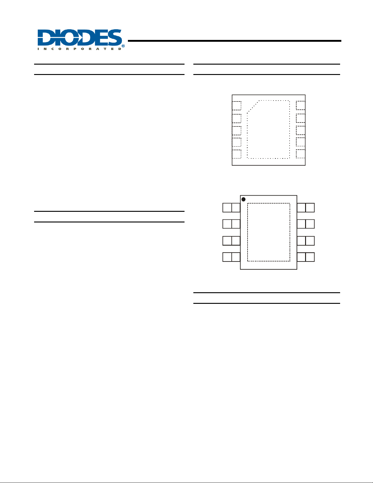
available in U-DFN3030-10 and SO-8EP packages.
Pin Assignments
IN
1
IN
2
3
POK
NC
4
EN
5
IN
1
Features
• Wide input voltage range: 2.2V – 5.5V
• 300mV very low dropout at 500mA load
• Very low quiescent current (I
• ± 2.5% total accuracy over line, load and temperature
• Adjustable output voltage range: 0.8V to 5.0V
• Very fast transient response
• High PSRR
• Accurate voltage regulation
• Current limiting and short circuit protection
• Thermal shutdown protection
• Stable with any type output capacitor ≥ 4.7µF
• Ambient temperature range -40ºC to +85°C
• U-DFN3030-10 and SO-8EP: Available in “Green”
Molding Compound (No Br, Sb)
• Lead Free Finish/RoHS Compliant (Note 1)
Notes: 1. EU Directive 2002/95/EC (RoHS). All applicable RoHS exemptions applied. Please visit our website at
http://www.diodes.com/products/lead_free.html.
): 125µA typical
Q
POK
EN
Applications
• Servers and laptops
• Smart phone and PDA
• MP3/MP4
• Bluetooth headset
• Low and medium power applications
• FPGA and DSP core or I/O power
IN
AP7165
Document number: DS31270 Rev. 7 - 2
1 of 15
www.diodes.com
2
3
4
(Top View)
U-DFN3030-10
(Top View)
SO-8EP
OUT
10
9
OUT
FB
8
NC
7
GND
6
8
OUT
7
OUT
6
FB
5
GND
March 2012
© Diodes Incorporated
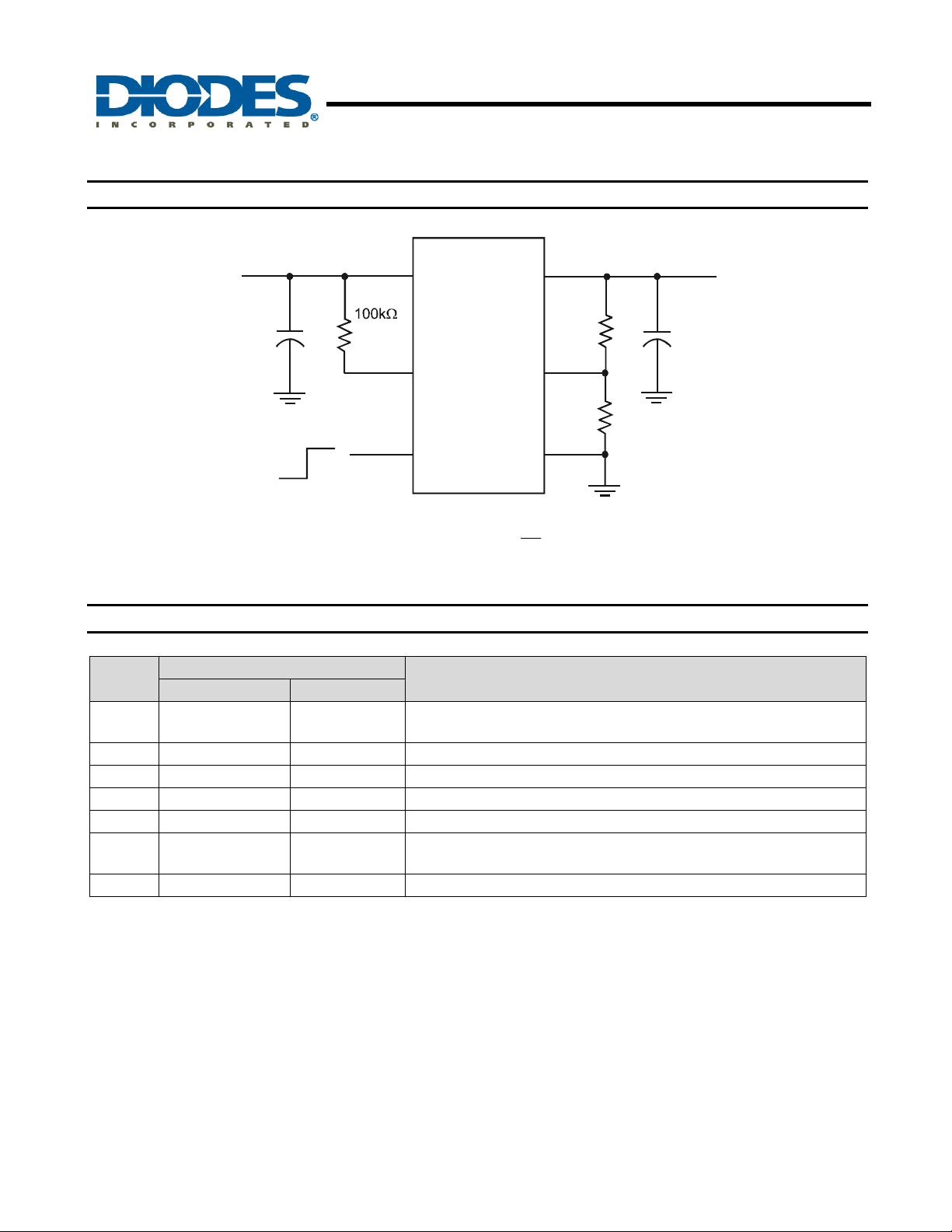
Typical Application Circuit
V
IN
AP7165
600mA LOW DROPOUT REGULATOR WITH POK
V
OUT
IN
OUT
1µF
Enable
POK
EN
AP7165
FB
GND
R
1
R
2
⎛
⎜
REFOUT
⎜
⎝
⎞
R
1
⎟
+=
1VV
⎟
R
2
⎠
Pin Descriptions
Name
IN 1, 2 1, 2
POK 3 3 Power-OK output, active-high open-drain.
EN 5 4 Enable input, active high.
GND 6 5 Ground.
FB 8 6 Output feedback.
OUT 9, 10 7, 8
NC 4, 7 NA No connection.
U-DFN3030-10 SO-8EP
Pin #
Description
Voltage input pins, to be tied together externally. Bypass to ground
through at least 1µF capacitor.
Voltage output pins, to be tied together externally. Bypass to ground
through at least 4.7µF ceramic capacitor.
10µF
AP7165
Document number: DS31270 Rev. 7 - 2
2 of 15
www.diodes.com
March 2012
© Diodes Incorporated
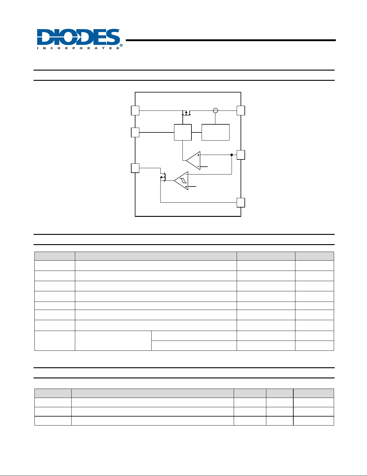
Functional Block Diagram
AP7165
600mA LOW DROPOUT REGULATOR WITH POK
IN
EN
POK
Gate
Driver
Current Limit
and Thermal
Shutdown
0.8V
0.744V
OUT
FB
GND
Absolute Maximum Ratings
Symbol Parameter Ratings Unit
ESD HBM Human Body Model ESD Protection 4 KV
ESD MM Machine Model ESD Protection 300 V
VIN
Input Voltage 7 V
V
OUT, FB, POK, EN Voltage
Continuous Load Current Internal Limited
T
Jmax
TST
PD
Notes: 2. Ratings apply to ambient temperature at 25°C
Maximum Junction Temperature 150 °C
Storage Temperature Range -65 ~ +150 °C
Power Dissipation
U-DFN3030-10 (Note 2, 4) 3.1 W
SO-8EP (Note 2, 5) 4.0 W
+0.3
IN
Recommended Operating Conditions
Symbol Parameter Min Max Unit
V
I
OUT
T
IN
A
Input voltage 2.2 5.5 V
Output Current 0 600 mA
Operating Ambient Temperature -40 +85 °C
AP7165
Document number: DS31270 Rev. 7 - 2
3 of 15
www.diodes.com
© Diodes Incorporated
V
March 2012
AP7165
Electrical Characteristics
(TA = 25oC, V
Symbol Parameter Test Conditions Min Typ. Max Unit
I
Q
I
SHDN
V
ROPOUT
V
REF
I
FB
V
OUT
ΔV
OUT
ΔV
IN
ΔV
/ V
OUT
tST
PSRR Power Supply Rejection Ratio
I
LIMIT
I
SHORT
V
V
I
EN
VOL
V
POK_TH_UP
V
POK_Hys
POK deglitch
I
POK_LK
T
SHDN
T
HYS
θ
JA
θ
JC
Notes: 3. POK pin must be disconnected from IN pin.
4. Test condition for U-DFN3030-10: Device mounted on FR-4 2-layer board, 2oz copper, with minimum recommended pad on top layer and 6 vias to
bottom layer 1.0”x1.5” ground plane.
5. Test condition for SO-8EP: Device mounted on 2" x 2" FR-4 substrate PCB, 2oz copper, with minimum recommended pad on top layer and
thermal vias to bottom layer ground plane.
IL
IH
= V
IN
OUT
+1V, C
= 1µF, C
IN
OUT
Input Quiescent Current
Input Shutdown Current
Dropout Voltage
FB reference voltage 0.8 V
FB leakage ⎯ 0.01 1 µA
Output Voltage Total Accuracy
OUT
V
/
Line Regulation
Load Regulation
OUT
Start-up Time, from EN high to POK
high
Current limit
Short-circuit Current
EN Input Logic Low Voltage 0.4 V
EN Input Logic High Voltage 1.4 V
EN Input leakage
POK output low voltage Force 2mA 100 200 mV
Output voltage (rising) POK threshold
Output voltage POK hysteresis 4%
POK leakage current
Thermal shutdown threshold 150 °C
Thermal shutdown hysteresis 25 °C
Thermal Resistance Junction-toAmbient
Thermal Resistance
Junction-to- Case
600mA LOW DROPOUT REGULATOR WITH POK
= 10µF, V
= VIN, unless otherwise stated)
EN
= 0
I
OUT
V
V
EN
OUT
= 0V, I
≥ 1.5V, I
= 0 (Note 3)
OUT
OU T
= 500mA
Over line, load and
temperature
V
= V
IN
I
OUT
I
OUT
V
EN
I
OUT
1kHz, V
V
OUT
V
OUT
VIN = 3.3V, V
V
EN
+1V to 5.5V,
OUT
= 1mA
from 1mA to 500mA
= 0V to 2.0V,
= 100mA, VIN = 3.3V
= 3.3V,
IN
= 1.2V, I
= 1.8V, R
OUT
OUT
= 0mA
OUT
< 0.2V
= 0.5Ω
= 0V or 5.5V
FB (or OUT for fixed version)
rising
V
= 3.3V, V
IN
V
POK
= 5.5V
OUT
= 1.2V
⎯ 125 170 µA
-1 0.01 +1 µA
300 400 mV
-2.5 +2.5 %
0.015 %/V
-1.0 +1.0 %
170 µs
60 dB
600 950 mA
380 mA
⎯ 0.01 1 µA
87% 92% 97%
150 µs
⎯ 0.01 1 µA
U-DFN3030-10 (Note 4) 40
SO-8EP (Note 5) 27
U-DFN3030-10 (Note 4) 9
SO-8EP (Note 5) 4
V
V
o
C/W
o
C/W
o
C/W
o
C/W
ref
ref
AP7165
Document number: DS31270 Rev. 7 - 2
4 of 15
www.diodes.com
March 2012
© Diodes Incorporated
OUTPU
T VOLTAG
OUTPU
T VOLTAG
Q
U
CEN
T CUR
REN
T
Q
U
C
T
CUR
R
T
Q
U
CENT
C
U
R
R
T
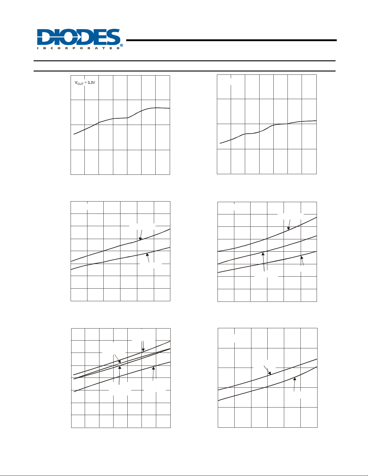
Typical Performance Characteristics
3.40
AP7165
600mA LOW DROPOUT REGULATOR WITH POK
1.90
V = 1.8V
OUT
3.35
E (V)
3.30
3.25
3.20
-50 -25 0 50 100 125
25 75
TEMPERATURE (°C)
Output Voltage vs. Temperature
170
V = 1.2V
OUT
160
150
(µA)
I = 300mA
OUT
140
130
120
IES
110
I = 0mA
OUT
100
1.85
E (V)
1.80
1.75
1.75
-50 -25 0 50 100 125
25 75
TEMPERATURE (°C)
Output Voltage vs. Temperature
170
V = 1.8V
OUT
160
I = 600mA
OUT
150
140
130
120
I = 300mA
110
QUIESCENT CURRENT (µA)
OUT
I = 0mA
OUT
100
90
-50 -25 0 100 12525 75
INPUT VOLTAGE ( V)
Quiesce nt Current vs. Input Voltage
150
140
V = 3.3V,
IN
V = 1.8V
(µA)
EN
EN
IES
130
120
110
100
90
OUT
V = 3.3V,
IN
V = 1.2V
OUT
V = 5.0V,
IN
V = 3.3V
OUT
V = 2.2V,
IN
V =1.0V
OUT
90
2.5 3.0 3.5 5.0 5.54.0 4.5
INPUT VOLTAGE (V)
Quiescent Current vs. Input Voltage
150
V = 1.8V
OUT
140
(µA)
V = 3.3V
EN
130
IN
120
IES
V = 2.5V
IN
110
80
70
-50 -25 0 50 100 12525 75
TEMPERATURE (°C)
Quiesce nt Current vs. Temperature
AP7165
Document number: DS31270 Rev. 7 - 2
5 of 15
www.diodes.com
100
0.0 0.1 0.2 0.3 0.5 0.60.4
I (A)
OUT
Quiesce nt C ur r ent vs. I
OUT
March 2012
© Diodes Incorporated
 Loading...