Diodes AP5100 User Manual

C
C
Y
Description
1.2A STEP-DOWN CONVERTER with 1.4MHz SWITCHING
Pin Assignments
The AP5100 is a current mode step-down converter with a
built-in power MOSFET to enable smallest solution size
power conversion.
With the low series resistance power switch it enables a
BST
constant output current of up to 1.2A over a wide input supply
range. The load and line regulation has excellent response
GND
time over the operating input voltage and temperature range.
The AP5100 is self protected, through a cycle-by-cycle
FB
current limiting algorithm and an on chip thermal protection.
The AP5100 will provide the voltage conversion with a low
count of widely available standard external components.
The AP5100 is available in SOT26 package.
Features
• VIN 4.75V to 24V
• Load current of up to 1.2A
• Internal Power MOSFET
• Stable with Low ESR Ceramic Output Capacitors
• Up to 90% Efficiency
• 0.1µA Shutdown Mode
Applications
• Distributed Power Systems
• Battery Charger
• Pre-Regulator for Linear Regulators
• WLED Drivers
• Fixed 1.4MHz Frequency
• Thermal Shutdown
• Cycle-by-Cycle Over Current Protection
• Resistor divider adjustable Output: 0.81V to 15V
• SOT26: Available in “Green” Molding Compound
(No Br, Sb)
• Lead Free Finish/RoHS Compliant (Note 1)
Notes: 1. EU Directive 2002/95/EC (RoHS). All applicable RoHS exemptions applied. Please visit our website at
http://www.diodes.com/products/lead_free.html.
Typical Application Circuit
100
(%)
IEN
EFFI
90
80
70
60
V = 12V
IN
L = 3.3µH
V = 5V
OUT
V = 3.3V
OUT
5
IN
AP5100
4
EN
GND
OFF
V
IN
C1
ON
( Top View )
1
2
3
SOT26
1
BST
6
SW
3
FB
AP5100
FREQUENCY
SW
6
5
IN
7
4
EN
C3
.L1
V
OUT
D1
R1
R2
C6
C2
50
40
LOAD CURRENT (A)
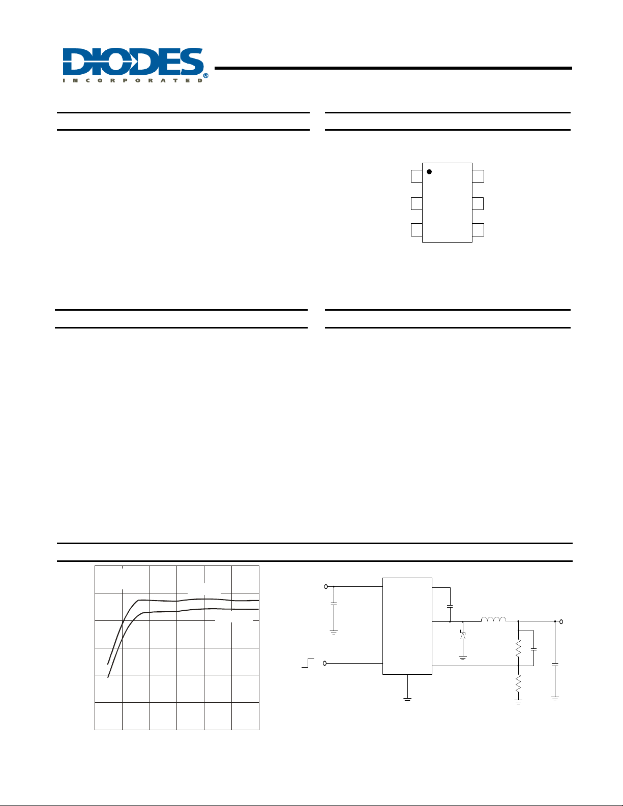
Fig. 1 Efficiency vs. Load Current
AP5100
Document number: DS32130 Rev. 3 - 2
0.6 0.8 1.0 1.200.20.4
1 of 12
www.diodes.com
Figure 2. Typical Application Circuit
April 2012
© Diodes Incorporated

Typical Application Circuit (cont.)
5
V
IN
10µF
OFF
C1
25V
R3
100kohm
ON
IN
4
EN
AP5100
1.2A STEP-DOWN CONVERTER with 1.4MHz SWITCHING
FREQUENCY
SW
FB
1
6
3
C3
22nF
D1
B230A
L1
3.3µH
R1
49.9kohm
R2
16.2kohm
C6
100pF
V
3.3V
C2
22µF
6.3V
OUT
BST
AP5100
GND
6V -12V
OFF
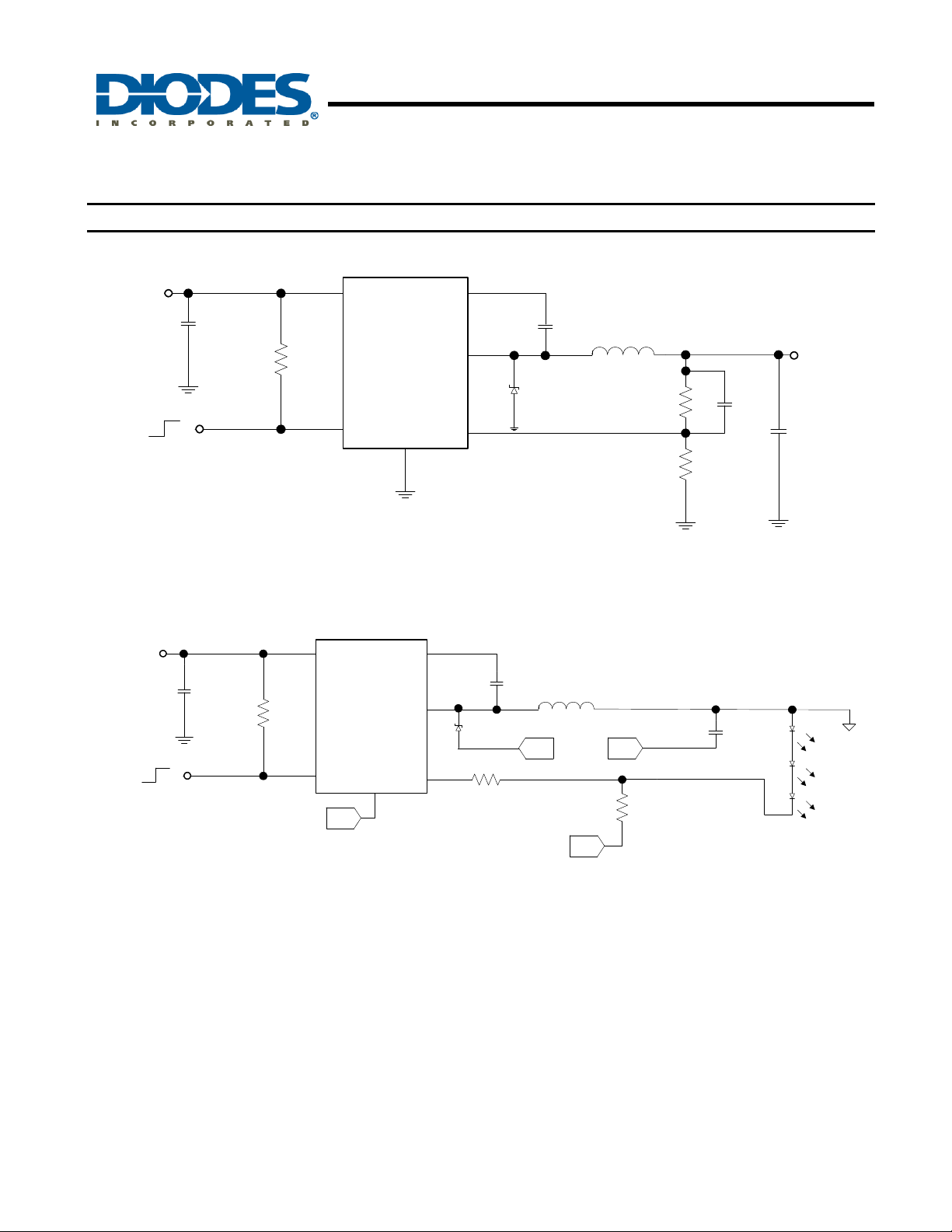
Figure 3. 1.4MHz, 3.3V Output at 1A Step-Down Converter
5
4
IN
AP5100
EN
- Vout
GND
Figure 4. White LED Driver Application
V
IN
C1
10µF
25V
ON
R3
100Kohm
BST
SW
FB
1
C3
10nF
6
3
200Kohm
D1
1N5819HW-7
- Vout -Vout
R4
1%
L1
10µH
40 ohm
-Vout
R2
1%
C2
10µF
16V
LED1
LED 2
LED 3
AP5100
Document number: DS32130 Rev. 3 - 2
2 of 12
www.diodes.com
April 2012
© Diodes Incorporated

1.2A STEP-DOWN CONVERTER with 1.4MHz SWITCHING
Pin Descriptions
Pin Name Pin #
Bootstrap. To form a boost circuit, a capacitor is connected between SW and BST pins to form a
BST 1
GND 2
FB 3
EN 4
IN 5
SW 6 Switch Output. This is the reference for the floating top gate driver.
floating supply across the power switch driver. This capacitor is needed to drive the power switch’s
gate above the supply voltage. Typical values for C
Ground. This pin is the voltage reference for the regulated output voltage. All control circuits are
referenced to this pin. For this reason care must be taken in its layout.
Feedback. To set the output voltage, connect this pin to the output resistor divider or directly to
V
. To prevent current limit run away during a current limit condition, the frequency foldback
OUT
comparator lowers the oscillator frequency when the FB voltage is below 400mV.
On/Off Control Input. Do not leave this pin floating. To turn the device ON, pull EN above 1.2V and
to turn it off pull below 0.4V.
If enable/disable is not used, connect a 100k resistor between EN to V
Supply Voltage. The AP5100 operates from a +4.75V to +24V unregulated input. A decoupling
capacitor C1 is required to prevent large voltage spikes from appearing at the input. Place this
capacitor near the IC.
Description
BST
Functional Block Diagram
range from 0.1µF to 1µF.
.
IN
AP5100
FREQUENCY
AP5100
Document number: DS32130 Rev. 3 - 2
Σ
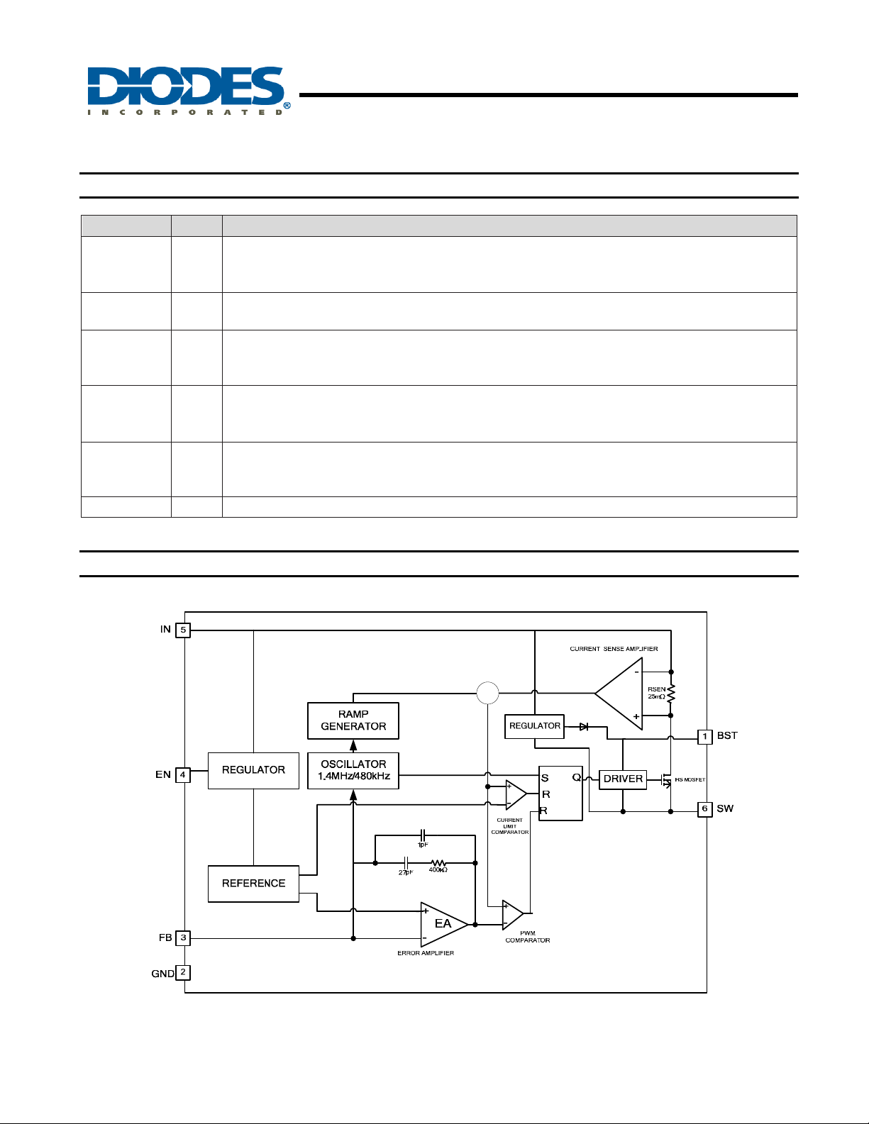
Figure 5. Functional Block Diagram
3 of 12
www.diodes.com
April 2012
© Diodes Incorporated

AP5100
Absolute Maximum Ratings (Note 2)
Symbol Description Rating Unit
ESD HBM Human Body Model ESD Protection 3 KV
ESD MM Machine Model ESD Protection 300 V
VIN
VSW
V
BST
TST
TJ
TL
JA
JC
Notes: 2. Exceeding these ratings may damage the device.
3. Test condition for SOT26: Measured on approximately 1” square of 1 oz copper.
Recommended Operating Conditions (Note 4)
Symbol Description Rating Unit
VIN
TA
V
OUT
Note: 4. The device function is not guaranteed outside of the recommended operating conditions.
AP5100
Document number: DS32130 Rev. 3 - 2
Supply Voltage
Switch Voltage
Boost Voltage
All Other Pins –0.3 to +6 V
Storage Temperature -65 to +150 °C
Junction Temperature +150 °C
Lead Temperature +260 °C
Junction to Ambient Thermal Resistance (Note 3) 140 °C/W
Junction to Case Thermal Resistance (Note 3) 35 °C/W
Supply Voltage 4.75 to 24 °C
Operating Ambient Temperature Range -25 to +85 °C
Output Voltage 0.81 to 15 V
1.2A STEP-DOWN CONVERTER with 1.4MHz SWITCHING
FREQUENCY
26
-0.3 to VIN +0.3
VSW +6
4 of 12
www.diodes.com
V
V
V
April 2012
© Diodes Incorporated
 Loading...