Diodes AP3988, AP3989, AP3990 User Manual

AP3988/89/90
Document number: DS36722 Rev. 3 - 2
1 of 13
www.diodes.com
March 2014
© Diodes Incorporated
AP3988/89/90
A Product Line of
Diodes Incorporated
NE W P R OD UC T
CPC
FB
VCC
CS
C
C
GND
1
2
3
4
7
6
5
Description
The AP3988/89/90 is a performance enhanced power switcher for
power supplies with better conversion efficiency, better voltage &
current accuracy, and improved protection functions. Typical
applications include charger, adapter for ADSL, home appliance
power supply, LED lighting power supply and PC auxiliary power
supplies. The controller regulates the output voltage and current in
the primary side by piece-wise Pulse Frequency Modulation (pPFM) in discontinuous conduction mode (DCM). The system
operating frequency reduces linearly from heavy load to light load
in each interval of the p-PFM, and enters constant current mode
when the load current equals to the maximum system output
current.
The AP3988/89/90 provides operating frequency dithering function
to improve EMC performance of power supply. The AP3988/89/90
also has built-in fixed cable voltage drop compensation (5% of
nominal system output voltage) and adjustable line voltage
compensation.
The AP3988/89/90 solution has fewer component number, smaller
size, and lower total cost.
The AP3988 is packaged in SO-7. The AP3989/90 is packaged in
PDIP-7.
Features
Primary Side Control for Eliminating Opto-coupler and
Secondary CV/CC Control Circuitry
Built-in NPN Transistor with 700V
CBO
Low Start-up Current: 0.2A (Typ.)
Internal Output Cable Voltage Drop Compensation
Hiccup Function to Improve Short Circuit Protection
Better Over Voltage Protection
Better Over Temperature Protection
Low Total Cost Solution
Output Power Range (Note 1):
AP3988 for 5.5W Adapter
AP3989 for 8W Adapter
AP3990 for 12W Adapter
Totally Lead-free & Fully RoHS Compliant (Note 2 & 3)
Halogen and Antimony Free. “Green” Device (Note 4)
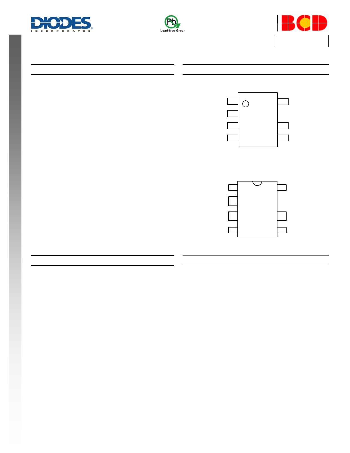
Pin Assignments
(Top View)
SO-7 (M Package) For AP3988
(Top View)
PDIP-7 (P7 Package) For AP3989/90
Applications
Adapters
Set Top Boxes
Auxiliary Supplies
Appliances
1
2
3
4
7
6
5
CPC
FB
VCC
CS
C
C
GND
PRIMARY SIDE POWER SWITCHER FOR OFF-LINE SMPS
Notes: 1. Typical continuous power in a non-ventilated enclosed adapter measured at +50°C ambient.
3. See http://www.diodes.com/quality/lead_free.html for more information about Diodes Incorporated’s definitions of Halogen- and Antimony-free, "Green"
and Lead-free.
4. Halogen- and Antimony-free "Green” products are defined as those which contain <900ppm bromine, <900ppm chlorine (<1500ppm total Br + Cl) and
<1000ppm antimony compounds.
2. No purposely added lead. Fully EU Directive 2002/95/EC (RoHS) & 2011/65/EU (RoHS 2) compliant.

AP3988/89/90
Document number: DS36722 Rev. 3 - 2
2 of 13
www.diodes.com
March 2014
© Diodes Incorporated
AP3988/89/90
A Product Line of
Diodes Incorporated
NE W P R OD UC T
+
J1
AC 90-264V
D1 to D4
C2
Rf1
+
C1
D6
L1
T1
FB
C
VCC
CS
+
C3
U1
CPC
C8
R5
C11
Np
Ns
Nfb
D5
C5
R6
Vo+
Vo-
C10
GND
D12
+
C12
R11
R12
C13
+
R10
R3
R8
R9
R7
L2
Item
Function
QTY
Item
Function
QTY
C1,C2
10µF/400V, electrolytic
2
U1
AP3990, PDIP-7
1
C3
4.7µF/50V, electrolytic
1
Rf1
2A/250V, fuse
1
C5
1nF/250V, ceramic
1
R3
3.3M/0.25W
1
C8
0.1µF, 0805
1
R5
3.9, 0805
1
C10
1nF/250VAC, Y1 capacitor
1
R6
150k, 0.25W
1
C11
1nF, 0805
1
R7
0.62, 1206
1
C12, C13
470µF/16V
2
R8
31k, 0805
1
D1 to D6
1N4007, rectifier diode
6
R9
13k, 0805
1
D12
MBR3100, Schottky diode
1
R10
360, 0805
1
L1
15mH, Common inductor, EE10
1
R11
27, 0805
1
L2
10µH/1A, inductor, 0805
1
R12
1.2k, 0805
1
– – –
T1
EE20 core, PC40, transformer
1
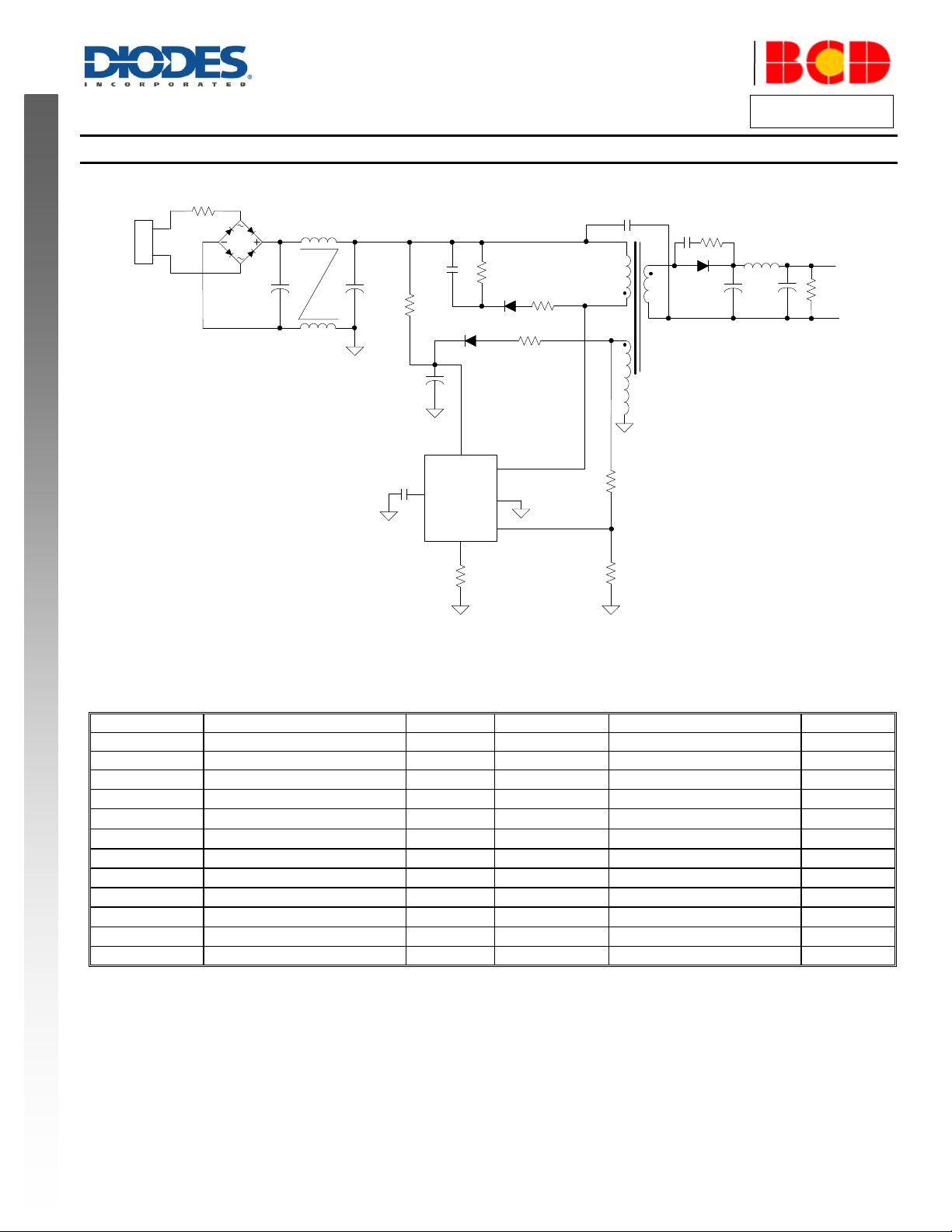
Typical Applications Circuit
For AP3990 (12V/1A)

AP3988/89/90
Document number: DS36722 Rev. 3 - 2
3 of 13
www.diodes.com
March 2014
© Diodes Incorporated
AP3988/89/90
A Product Line of
Diodes Incorporated
NE W P R OD UC T
Pin Number
Pin Name
Function
1
CPC
This pin connects a capacitor to GND for output cable compensation
2
FB
The voltage feedback from auxiliary winding
3
VCC
This pin receives rectified voltage from the auxiliary winding of the transformer
4
CS
Current sense for primary side of transformer
5, 6
C
This pin is connected with an internal power BJT’s collector
7
GND
This pin is the signal reference ground
Regulator
&
Bias
OVP
OCkP
OTP
PFM
UVLO
CV_ctrl
PFM
Driver
R
Q
S
R
Q
S
FB
CS
CPC
VCC
CS
GND
Constant Voltage Control
Cable Compensation
Constant Current
Control
0.05V
V
FB_ref
3
4
7
1
2
V
CSN(N=1,2,3)
COMP
Peak Current Control
LEB
Frequency Dither
V
CSN
Select
Dynamic
Response
Pro
Dyn
Shutdown
Pre_Shutdown
Line
Comp.
t
ONS
t
ONS
, NL and LL
Detector
OSC
UV
UV
Vload
Vally
ON
Vload
CC_ctrl
Max Tonp
Rcs Short
Output Short
t
ONS
LL
NL
CPC
t
OSC
Detect
Pulse
(LL+NL)Bar
NL
Vload
UV
CV_M
DetectON
DetectON
LL
Vload
V
CSN(N=1,2,3)
tosc
NL LL
C
5, 6
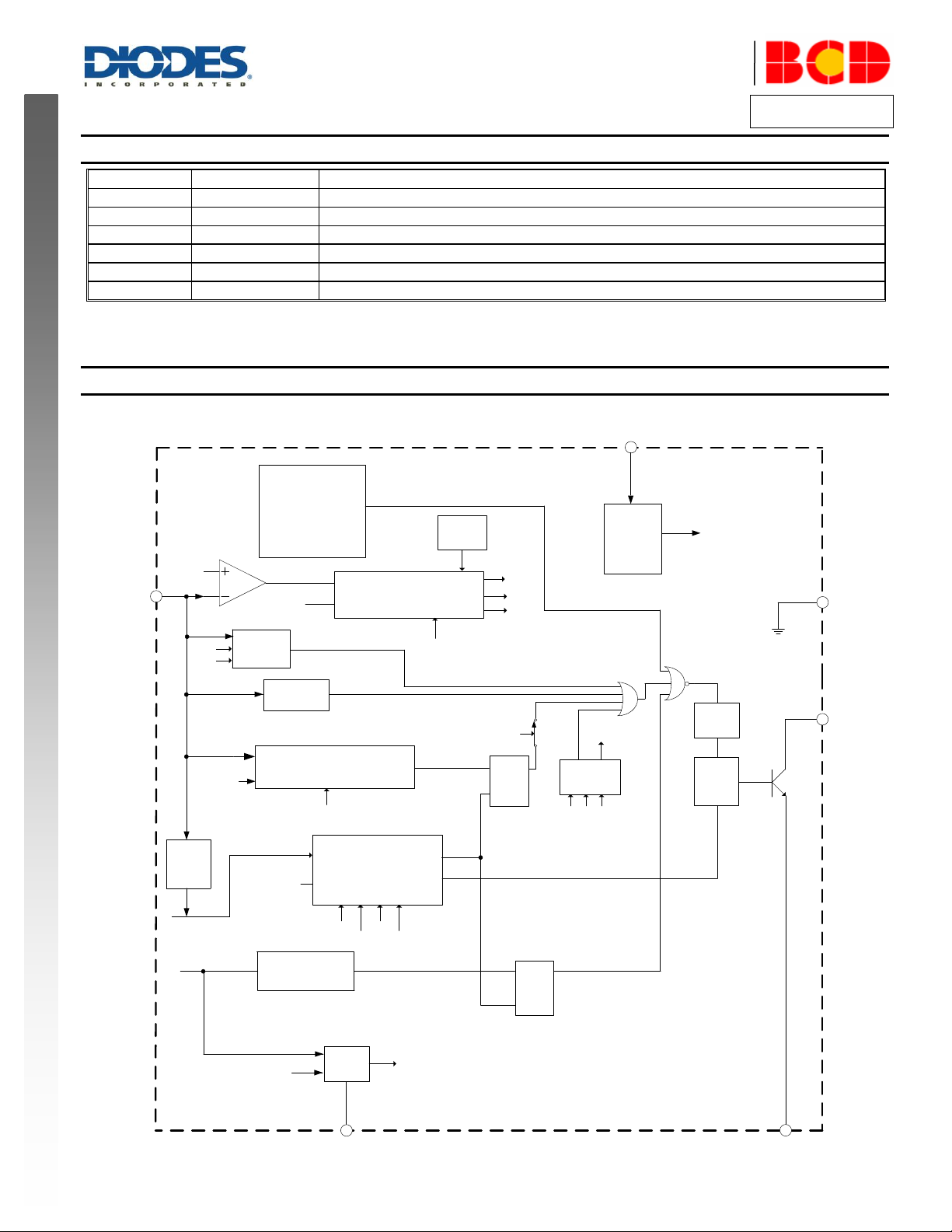
Pin Descriptions
Functional Block Diagram

AP3988/89/90
Document number: DS36722 Rev. 3 - 2
4 of 13
www.diodes.com
March 2014
© Diodes Incorporated
AP3988/89/90
A Product Line of
Diodes Incorporated
NE W P R OD UC T
Symbol
Parameter
Rating
Unit
VCC
Supply Voltage
-0.3 to 30
V
VCS, V
CPC
Voltage on CS, CPC Pin
-0.3 to 7
V
VFB
FB Input Voltage
-0.3 to 8
V
V
CBO
Collector-emitter Voltage
700
V
I
CDC
Collector DC Current
AP3988/89
1.5
A
AP3990
4
TJ
Operating Junction Temperature
+150
°C
T
STG
Storage Temperature
-65 to +150
°C
T
LEAD
Lead Temperature (Soldering, 10 sec)
+300
°C
–
ESD (Machine Model)
200
V
–
ESD (Human Body Model)
2000
V
PD
Total Power Dissipation
AP3988
0.7
W
AP3989
0.9
AP3990
1.1
Symbol
Parameter
Min
Max
Unit
VCC
Supply Voltage
–
25
V
TOP
Operating Temperature Range
-40
+85
°C
f
S(MAX)
Maximum Operating Frequency
–
60
kHz
Symbol
Parameter
Value
Unit
θ
JA
Junction to Ambient
AP3988
100
°C/W
AP3989
80
AP3990
65
θ
JC
Junction to Case
AP3988
50
AP3989
40
AP3990
35
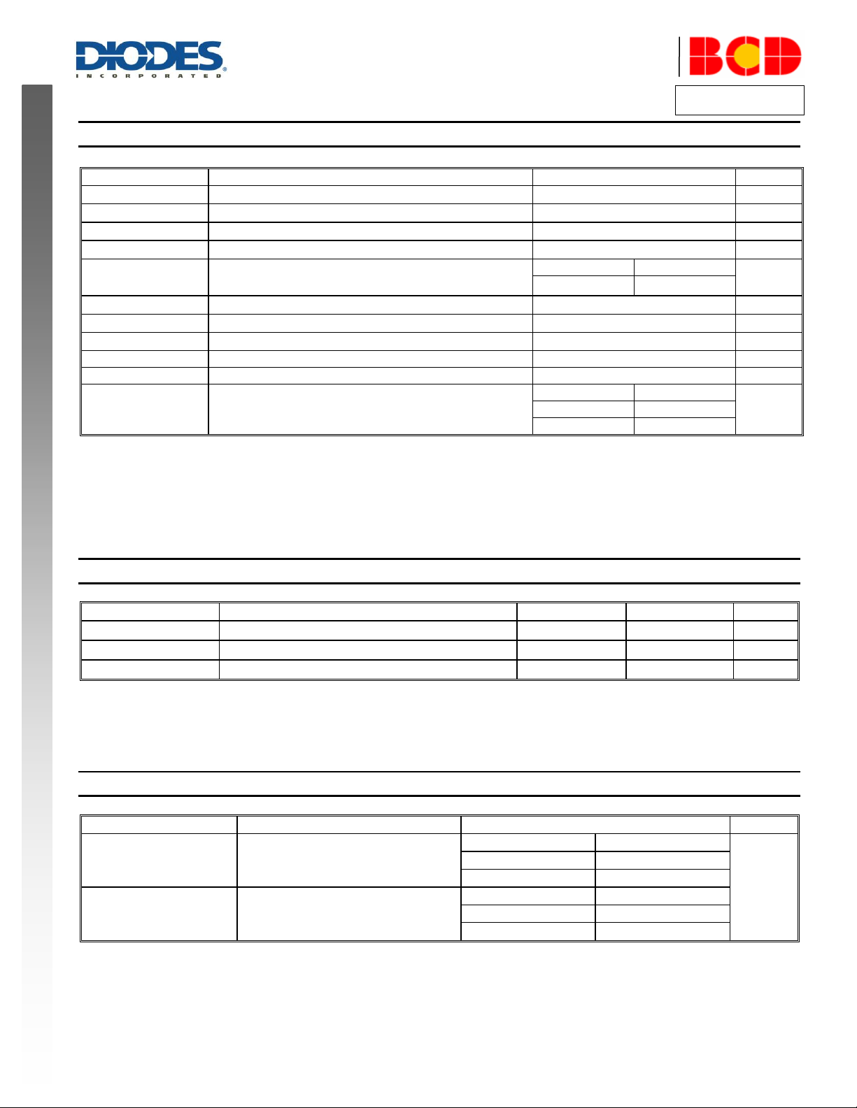
Absolute Maximum Ratings (Note 5)
Note 5: Stresses greater than those listed under “Absolute Maximum Ratings” may cause permanent damage to the device. These are stress ratings only, and
functional operation of the device at these or any other conditions beyond those indicated under “Recommended Operating Condi tions” is not implied.
Exposure to “Absolute Maximum Ratings” for extended periods may affect device reliability.
Recommended Operating Conditions
Thermal Impedance (Note 6)
Note 6: When mounted a standard single-sided FR4 board with 300mm2 Cu (at least 35µm thick) connected to all collectors and CS pins.
 Loading...