A
V
Green
SINGLE SLEW RATE CONTROLLED LOAD SWITCH
Description
The AP2281 slew rate controlled load switch is a single P-channel
MOSFET power switch designed for high-side load-switching
applications. The MOSFET has a typical R
allowing increased load current handling capacity with a low forward
voltage drop. The turn-on slew rate of the device is controlled
internally.
The AP2281 load switch is designed to operate from 1.5V to 6V,
making it ideal for 1.8V, 2.5V, 3.3V, and 5V systems. The typical
quiescent supply current is only 0.01µA.
of 80m at 5V,
DS(ON)
Features
Wide input voltage range: 1.5V – 6V
Low R
Turn-on slew rate controlled
AP2281-1: 1ms turn-on rise time
AP2281-3: 100µs turn-on rise time with internal discharge
Very low turn-on quiescent current: << 1µA
Fast load discharge option
Temperature range -40°C to +85°C
Lead-Free Finish; RoHS Compliant (Notes 1 & 2)
Halogen and Antimony Free. “Green” Device (Note 3)
: 80mΩ typical @ 5V
DS(ON)
Applications
Smart Phones
PDA
Cell Phones
GPS Navigators
PMP/MP4
Notebook and Pocket PC
Notes: 1. EU Directive 2002/95/EC (RoHS) & 2011/65/EU (RoHS 2) compliant. All applicable RoHS exemptions applied.
2. See http://www.diodes.com/quality/lead_free.html for more information about Diodes Incorporated’s definitions of Halogen- and Antimony-free, "Green"
and Lead-free.
3. Halogen- and Antimony-free "Green” products are defined as those which contain <900ppm bromine, <900ppm chlorine (<1500ppm total Br + Cl) and
<1000ppm antimony compounds.
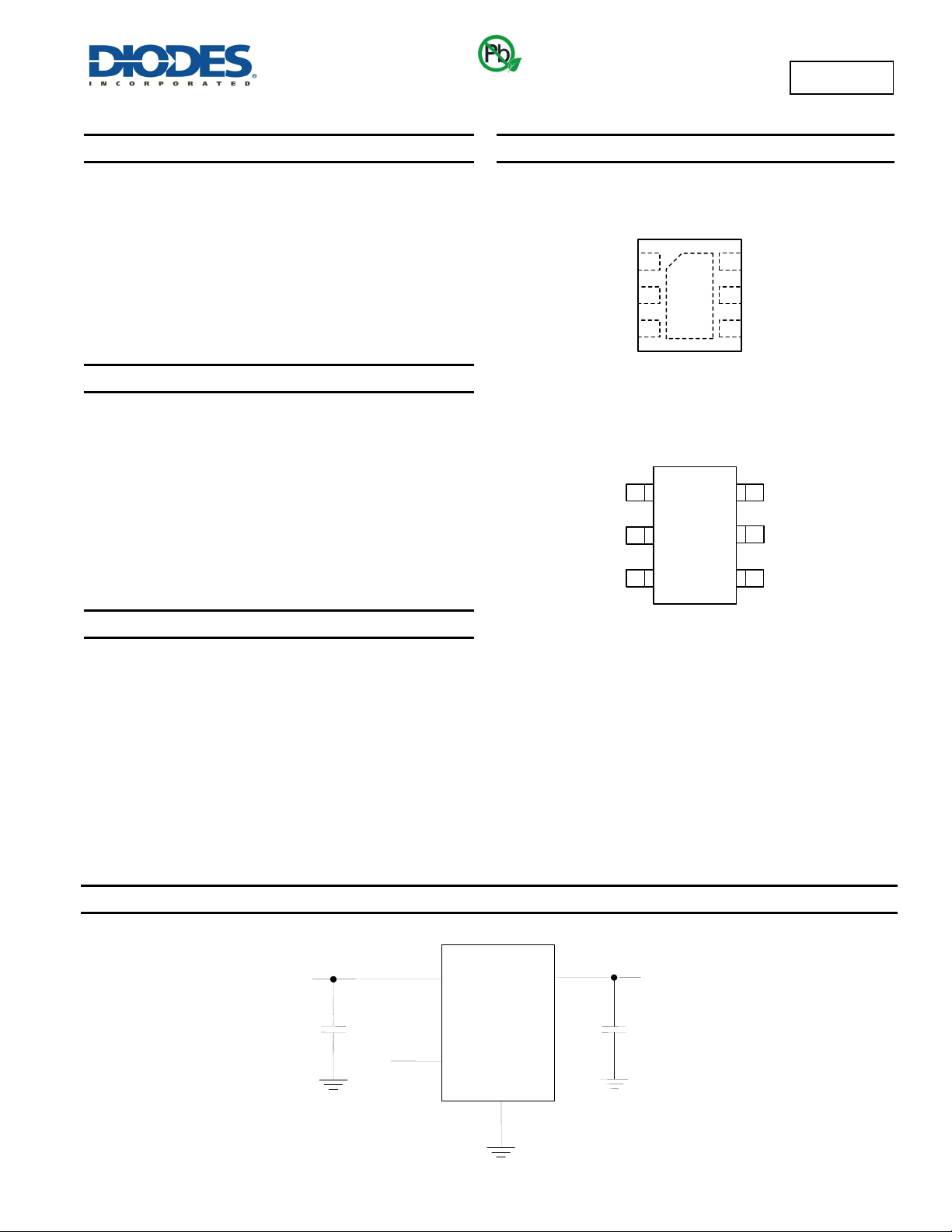
Pin Assignments
OUT
GND
EN IN
( Top View )
1
IN
2
IN
3
EN
U-DFN2018-6
1
2
7
(Top View)
SOT26
6
OUT
5
OUT
4
GND
IN
6
GND
5
43
P2281
Typical Applications Circuit
AP2281
Document number: DS31359 Rev. 7 - 2
IN
1uF
IN
Enable
EN
OUT
GND
OUT
V
0.1uF
1 of 11
www.diodes.com
November 2013
© Diodes Incorporated

A
Pin Descriptions
P2281
Pin Name
OUT
GND 2, 5 4 Ground.
EN 3 3 Enable input, active high
IN
PAD 7 Thermal pad. Suggest connecting to ground plane to get better heat dissipation.
Pin Number
SOT26 U-DFN2018-6
1 5, 6
4, 6 1, 2
Voltage output pin. This is the pin to the P-channel MOSFET drain connection. Bypass to ground
through a 0.1uF capacitor.
Voltage input pin. This is the pin to the P-channel MOSFET source. Bypass to ground through a
1µF capacitor.
Function
Options
Part Number Slew Rate (typ) Active Pull Down Enable
AP2281-1 1ms No Active High
AP2281-3 100µs Yes Active High
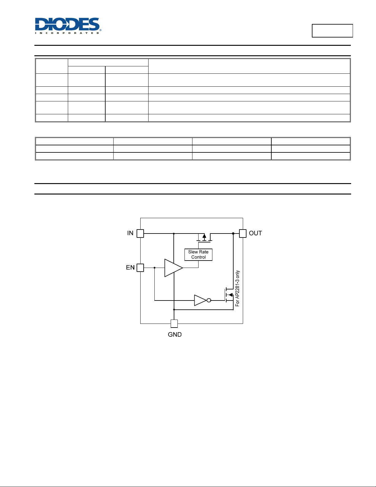
Functional Block Diagram
AP2281
Document number: DS31359 Rev. 7 - 2
2 of 11
www.diodes.com
November 2013
© Diodes Incorporated

A
P2281
Absolute Maximum Ratings (@T
= +25°C, unless otherwise specified.)
A
Symbol Parameter Ratings Unit
ESD HBM Human Body Model ESD Protection 5 KV
ESD MM Machine Model ESD Protection
V
IN
V
OUT
V
EN
I
load
T
J
T
ST
P
D
Notes: 4. TJ, max = +125°C.
5. Ratings apply to ambient temperature at +25°C.
Stresses greater than the 'Absolute Maximum Ratings' specified above, may cause permanent damage to the device. These are stress ratings only; functional
operation of the device at these or any other conditions exceeding those indicated in this specification is not implied. Device reliability may be affected by exposure to
absolute maximum rating conditions for extended periods of time.
Input Voltage 6.5 V
Output Voltage VIN +0.3 V
Enable Voltage 6.5 V
Maximum Continuous Load Current 2 A
Operating Junction Temperature Range -40 to +125 °C
Storage Temperature Range -65 to +150 °C
Power Dissipation
SOT26 (Note 4, 5, 6) 720 mW
U-DFN2018-6 (Note 4, 5, 7) 1410 mW
SOT26 500 V
U-DFN2018-6 450 V
Recommended Operating Conditions (@T
= +25°C, unless otherwise specified.)
A
Symbol Parameter Min Max Unit
V
I
OUT
T
IN
A
Input voltage 1.5 6.0 V
Output Current 0 2.0 A
Operating Ambient Temperature -40 +85 °C
Electrical Characteristics (@T
= +25°C, unless otherwise specified.)
A
Symbol Parameters Test Conditions Min Typ Max Unit
I
SHDN
I
LEAK
R
DS(ON)
V
V
I
SINK
T
D(ON)
T
T
D(OFF)
R
DISCH
θJA
θJC
I
ON
Q
Input Quiescent Current
Input Shutdown Current
Input Leakage Current
Switch on-resistance
V
= VIN, I
EN
V
= 0V, OUT open
EN
V
= 0V, OUT grounded
EN
= 5.0V
V
IN
OUT
= 0
VIN = 3.3V
VIN = 1.8V
VIN = 1.5V
IL
IH
EN Input Logic Low Voltage
EN Input Logic High Voltage
EN Input leakage
Output turn-on delay time
Output turn-on rise time
Output turn-off delay time
Discharge FET on-resistance
V
= 1.5V to 6V
IN
1.5V ≤ V
≤ 2.7V
IN
2.7V < VIN < 5.25V
V
≥ 5.25V
IN
V
= 5V
EN
R
= 10Ω
LOAD
AP2281-1, R
AP2281-3, R
R
= 10Ω
LOAD
LOAD
LOAD
= 10Ω
= 10Ω
For AP2281-3 only, V
= GND
EN
SOT26 (Note 6)
Thermal Resistance Junction-to-Ambient
U-DFN2018-6 (Note 7)
SOT26 (Note 6)
Thermal Resistance Junction-to-case
U-DFN2018-6 (Note 7)
— 0.01 1 μA
—
—
—
—
—
—
— —
1.4
1.6
1.7
— —
—
—
—
—
—
—
—
—
—
0.01 1 μA
0.01 1 μA
80 100 mΩ
95 120
160 210
mΩ
mΩ
210 280 mΩ
0.4 V
— —
— —
— —
1 μA
1 — μS
1000 1500 μS
100 150 μS
0.5 1 μS
65 100 Ω
153
78
29
19
—
—
—
—
°C/W
°C/W
V
V
V
Notes: 6. Test condition for SOT26: Device mounted on FR-4 substrate PC board, 2oz copper, with minimum recommended pad layout.
7. Test condition for U-DFN2018-6: Device mounted on FR-4 2-layer board, 2oz copper, with minimum recommended pad on top layer and 3 vias to bottom
layer 1.0"x1.4" ground plane.
AP2281
Document number: DS31359 Rev. 7 - 2
3 of 11
www.diodes.com
November 2013
© Diodes Incorporated

A
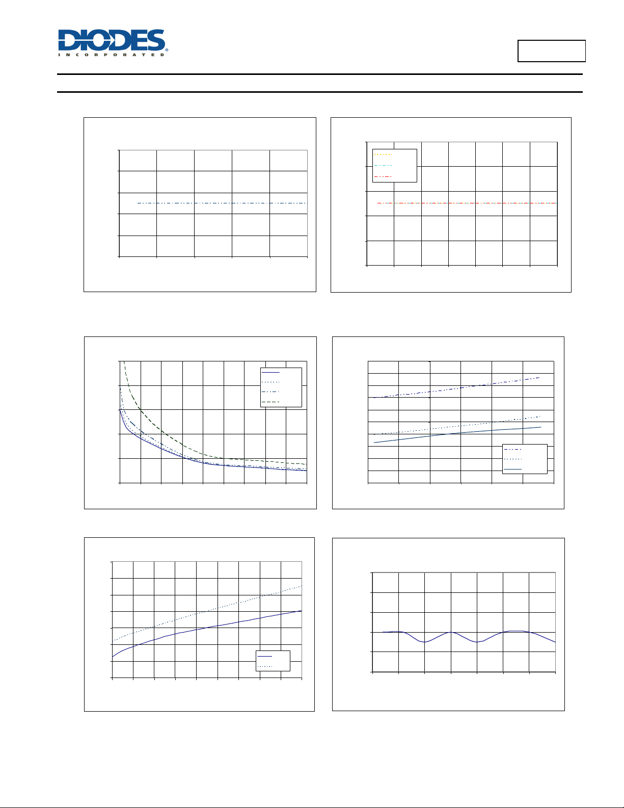
Typical Performance Characteristics
P2281
Quiescent Current vs. Input Voltage
0.01
A)
0.008
0.006
0.004
0.002
Quiescent Current (
0
1.02.0 3.04.0 5.06.0
Inpu t Voltage (V)
R
vs. Input Voltage
DS( ON)
I=100mA
I=500mA
I=1A
I=2A
)
300.00
250.00
200.00
(m
150.00
DS(ON)
R
100.00
50.00
1.522.533.544.555.56
Input Voltage (V)
Quiescent Current vs. Temperature
0.010
A)
0.008
0.006
0.004
0.002
VIN=1.8V
VIN=3.3V
VIN=5.0V
Quiescent Current (
0.000
-50 -25 0 25 50 75 100 125
Temperature (°C)
R
vs. Temperature
DS( ON)
200.00
180.00
160.00
140.00
)
120.00
(m
100.00
80.00
DS(ON)
R
60.00
40.00
20.00
0.00
-50 -25 0 25 50 75 100
Temperature (°C)
VIN =1.8V
VIN =3.3V
VIN =5V
ENABLE Threshold vs. Input Voltage
1.8
1.6
1.4
1.2
1.0
0.8
ON/OFF Threshold (V)
0.6
0.4
1.5 2.0 2.5 3.0 3.5 4.0 4.5 5.0 5.5 6.0
AP2281
Document number: DS31359 Rev. 7 - 2
Input Voltage (V )
VIL (V)
VIH (V)
4 of 11
www.diodes.com
Input Shutdown Current vs. Temperature
0.010
0.008
A)
0.006
(
0.004
SHDN
I
0.002
0.000
-50 -25 0 25 50 75 100 125
Temperature (°C)
November 2013
© Diodes Incorporated
 Loading...