

Page 1
AP2162/AP2172
1A DUAL CHANNEL CURRENT-LIMIT ED POWER
SWITCH
Features
• Dual USB port power switches
• Over-current and thermal protection
• 1.5A accurate current limiting
• Reverse Current Blocking
• 115m
• Input voltage range: 2.7V – 5.5V
• 0.6ms typical rise time
• Very low shutdown current: 1uA (max)
• Fault report (FLG) with blanking time (7ms typ)
• ESD protection: 4.5KV HBM, 350V MM
• Active high (AP2172) or active low (AP2162) enable
• Ambient temperature range -40ºC to 85°C
• SOP-8L and MSOP-8L-EP (Exposed Pad): Available in
• Lead Free Finish / RoHS Compliant (Note 1)
• UL Recognized, File Number E322375
• IEC60950-1 CB Scheme Certified
on-resistance
“Green” Molding Compound (No Br, Sb)
Description
The AP2162 and AP2172 are integrated high-side power switches
optimized for Universal Serial Bus (USB) and other hot-swap
applications. The family of devices complies with USB 2.0 and
available with both polarities of Enable input. They offer current
and thermal limiting and short circuit protection as well as
controlled rise time and under-voltage lockout functionality.
A 7ms deglitch capability on the open-drain Flag output prevents
false over-current reporting and does not require any external
components.
All devices are available in SOP-8L and MSOP-8L-EP packages.
Applications
• Consumer electronics – LCD TV & Monitor, Game Machines
• Communications – Set-Top-Box, GPS, Smartphone
• Computing – Laptop, Desktop, Servers, Printers, Docking Station, HUB
Ordering Information
AP 21 X 2 XX G - 13
Green
G : Green
6 : Active Low
7 : Active High
Channel
2 : 2 Channel
PackageEnable
S : SOP-8L
MP : MSOP-8L-EP
Device
Package
Code
Packaging
(Note 2)
Quantity Part Number Suffix
AP21X2SG-13 S SOP-8L 2500/Tape & Reel -13
AP21X2MPG-13 MP MSOP-8L-EP 2500/Tape & Reel -13
Notes: 1. EU Directive 2002/95/EC (RoHS). All applicable RoHS exemptions applied. Please visit our website at
http://www.diodes.com/products/lead_free.html
2. Pad layout as shown on Diodes Inc. suggested pad layout document AP02001, which can be found on our website at
http://www.diodes.com/datasheets/ap02001.pdf
.
.
AP2162/AP2172 Rev. 5 1 of 17 FEBRUARY 2009
www.diodes.com © Diodes Incorporated
13” Tape and Reel
Packing
13 : Tape & Reel
Page 2
Pin Assignment
( Top View )
IN
1
2
3
4
SOP-8L
GND
EN1
EN2
AP2162/AP2172
1A DUAL CHANNEL CURRENT-LIMIT ED POWER
SWITCH
( Top View )
8
FLG1
1
2
3
4
MSOP-8L-EP
7
6
5
OUT1
OUT2
FLG2
GND
IN
EN1
EN2
8
FLG1
7
OUT1
6
OUT2
5
FLG2
Pin Descriptions
Pin Name
GND 1 Ground
IN
EN1 3 Switch 1 enable input, active low (AP2162) or active high ( AP2172 )
EN2 4 Switch 2 enable input, active low (AP2162) or active high (AP2172)
FLG2 5
OUT2
OUT1
FLG1 8
Pin
Number
2 Voltage input pin
Switch 2 over-current and over-temperature fault report; open-drain flag is active
low when triggered
6 Switch 2 voltage output pin
7 Switch 1 voltage output pin
Switch 1 over-current and over-temperature fault report; open-drain flag is active
low when triggered
Descriptions
AP2162/AP2172 Rev. 5
www.diodes.com © Diodes Incorporated
2 of 17 FEBRUARY 2009
Page 3
Functional Block Diagram
AP2162, AP2172
EN1
UVLO
Thermal
Sense
Driver
AP2162/AP2172
1A DUAL CHANNEL CURRENT-LIMIT ED POWER
SWITCH
FLG1
Deg litc h
Cu rrent
Limit
GND
IN
UVLO
EN2
T ypical Application Circuit
AP2172 Enable Active High
Power Supply
2.7V to 5.5V
10k
10k
10uF
Driver
Thermal
Sense
0.1uF
IN
Current
Sense
Current
Sense
Current
Limit
OUT1
Deg litc h
0.1uF
68uF
GND
OUT1
OUT2
FLG2
Load
OFF
ON
FLG1
FLG2
EN1
EN2
GND
OUT2
0.1uF
68uF
Load
Available Options
Recommended
Maximum Continuous
Load Current
Part Numb er Channel Enable Pin (EN)
Current Limit
(Typical)
AP2162 2 Active Low 1.5A 1.0A
AP2172 2 Active High 1.5A 1.0A
AP2162/AP2172 Rev. 5
3 of 17 FEBRUARY 2009
www.diodes.com © Diodes Incorporated
Page 4
AP2162/AP2172
1A DUAL CHANNEL CURRENT-LIMIT ED POWER
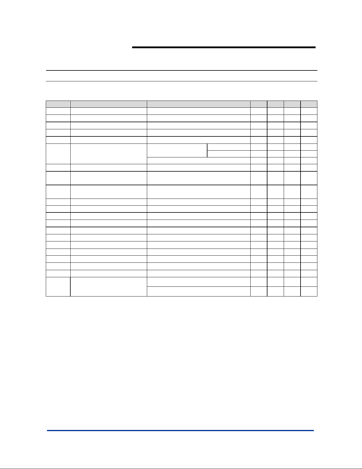
Absolute Maximum Ratings
Symbol Parameter Ratings Units
ESD HBM Human Body Model ESD Protection 3 KV
ESD MM Machine Model ESD Protection 300 V
VIN Input Voltage 6.5 V
V
Output Voltage VIN + 0.3
OUT
V
EN , VFLG
Notes: 3. UL Recognized Rating from -30°C to 70°C (Diodes qualified TST from -65°C to 150°C)
Recommended Operating Conditions
Symbol Parameter Min Max Units
Enable Voltage 6.5 V
I
Maximum Continuous Load Current Internal Limited A
load
T
Maximum Junction Temperature 150 °C
Jmax
TST Storage Temperature Range (Note 3) -65 to 150 °C
V
I
OUT
T
IN
A
Input voltage 2.7 5.5 V
Output Current 0 1.0 A
Operating Ambient T emperature -40 85
SWITCH
V
°C
AP2162/AP2172 Rev. 5
www.diodes.com © Diodes Incorporated
4 of 17 FEBRUARY 2009
Page 5
μ
AP2162/AP2172
1A DUAL CHANNEL CURRENT-LIMIT ED POWER
SWITCH
Electrical Characteristics
= 25oC, V
(T
A
Symbol Parameter Test Conditions Min Typ. Max Unit
V
UVLO
I
SHDN
I
Q
I
LEAK
I
Reverse Leakage Current Disabled, VIN = 0V, V
REV
R
DS(ON)
I
SHORT
I
Over-Load Current Limit
LIMIT
I
Trig
V
IL
V
IH
I
SINK
T
D(ON)
TR Output turn-on rise time
T
D(OFF)
TF Output turn-off fall time
R
FLG
T
FLG blanking time
Blank
T
SHDN
T
HYS
θ
JA
Notes: 4. Test condition for SOP-8L: Device mounted on FR-4 2-layer board, 2oz copper, with minimum recommended pad layout.
5. Test condition f or MSOP-8L-EP: Device mounted on FR-4 2-layer board, 2oz copper, with minimum recommended pad on top layer and 3
vias to bottom layer ground plane.
= +5.0V, unless otherwise stated)
IN
Input UVLO R
Input Shutdown Current Disabled, I
Input Quiescent Current, Dual Enabled, I
=1k 1.6 1.9 2.5 V
load
= 0 0.5 1
OUT
= 0 100 160
OUT
Input Leakage Current Disabled, OUT grounded 1
Switch on-resistance
Short-circuit current limit
Current limiting trigger
threshold
= 5V, I
OUT
V
= 5V, I
IN
o
C TA 85oC
-40
VIN = 3.3V, I
= 0.5A,
OUT
= 0.5A, -40oC TA85oC 140 180 m
OUT
MSOP-8L-EP
SOP-8L
Enabled into short circuit, C
V
= 5V, V
IN
T
85oC
A
= VEN, Output Current Slew rate
V
IN
(<100A/s), C
= 4.6V, CL=68μF, -40oC
OUT
=68μF
L
at VIN 1
REV
115 150 m
120 160 m
=68μF
L
1.4 A
1.1 1.5 1.9 A
2.4 A
EN Input Logic Low Voltage VIN = 2.7V to 5.5V 0.8 V
EN Input Logic High Voltage VIN = 2.7V to 5.5V 2 V
EN Input leakage V
Output turn-on delay time
Output turn-off delay time
FLG output FET on-resistance I
Thermal shutdown threshold Enabled, R
= 5V 1
EN
C
=1μF, R
L
C
=1μF, R
L
C
=1μF, R
L
=1μF, R
C
L
=10mA 30 50
FLG
=10μF, CL=68μF
C
IN
=10
load
=10
load
=10
load
=10
load
=1k 140
load
0.05 ms
0.6 1.5 ms
0.01 ms
0.05 0.1 ms
4 7 15 ms
Thermal shutdown hysteresis 25
Thermal Resistance
Junction-to-Ambient
SOP-8L (Note 4) 110
MSOP-8L-EP (Note 5) 60 oC/W
μA
μA
μA
μA
°C
°C
o
C/W
A
AP2162/AP2172 Rev. 5
5 of 17 FEBRUARY 2009
www.diodes.com © Diodes Incorporated
Page 6
1A DUAL CHANNEL CURRENT-LIMIT ED POWER
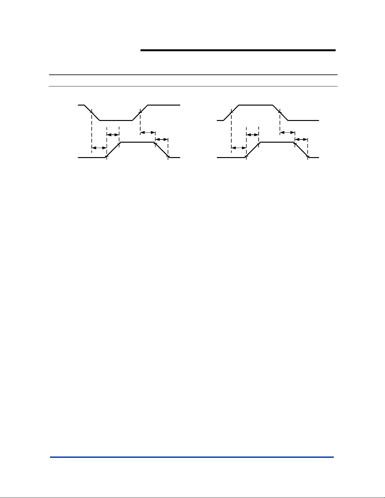
Typical Performance Characteristics
AP2162/AP2172
SWITCH
V
EN
V
OUT
T
50%
D(ON)
T
10%
50%
T
R
90%
D(OFF)
90%
Figure 1. Voltage Waveforms: AP2162 (left), AP2172 (right)
All Enable Plots are for AP2172 Active High
Channel 1 Turn-On Delay and Rise Time
Ven 1
5V/div
Vout 1
2V/div
500us/div
Channel 2 Turn-On Delay and Rise Time
10%
T
F
CL=1uF
TA=25°C
RL=10
V
EN
50%
T
T
D(ON)
V
OUT
10%
50%
R
90%
Channel 1 Turn-Off Delay and Fall Time
Ven 1
5V/div
Vout 1
2V/div
500us/div
Channel 2 Turn-Off Delay and Fall Time
T
D(OFF)
90%
10%
T
F
CL=1uF
TA=25°C
RL=10
Ven 2
5V/div
Vout 2
2V/div
CL=1uF
TA=25°C
RL=10
500us/div
AP2162/AP2172 Rev. 5
www.diodes.com © Diodes Incorporated
Ven 2
5V/div
CL=1uF
Vout 2
2V/div
TA=25°C
RL=10
500us/div
6 of 17 FEBRUARY 2009
Page 7

1A DUAL CHANNEL CURRENT-LIMIT ED POWER
Typical Performance Characteristics (Continued)
Channel 1 Turn-On Delay and Rise Time
Channel 1 Turn-Off Delay and Fall Time
AP2162/AP2172
SWITCH
Ven 1
5V/div
Vout 1
2V/div
500us/div
Channel 2 Turn-On Delay and Rise Time
Ven 2
5V/div
Vout 2
2V/div
500us/div
Channel 1 Short Circuit Current,
Device Enabled Into Short
CL=100uF
TA=25°C
RL=10
CL=100uF
TA=25°C
RL=10
Ven 1
5V/div
CL=100uF
Vout 1
2V/div
TA=25°C
RL=10
500us/div
Channel 2 Turn-Off Delay and Fall Time
Ven 2
5V/div
CL=100uF
Vout 2
2V/div
TA=25°C
RL=10
500us/div
Channel 2 Short Circuit Current,
Device Enabled Into Short
Ven 1
5V/div
Iout 1
500mA/div
VIN=5V
TA=25°C
CL=68uF
500us/div
AP2162/AP2172 Rev. 5
www.diodes.com © Diodes Incorporated
Ven 2
5V/div
Iout 2
500mA/div
VIN=5V
TA=25°C
CL=68uF
500us/div
7 of 17 FEBRUARY 2009
Page 8

1A DUAL CHANNEL CURRENT-LIMIT ED POWER
Typical Performance Characteristics (Continued)
Channel 1 Inrush Current
Channel 2 Inrush Current
AP2162/AP2172
SWITCH
Ven 1
5V/div
Iout 1
200mA/div
=100uF
C
L
C
=220uF
L
CL=470uF
1ms/div
Channel 1
1 Ω Load Connected to Enabled Device
Vflag 1
2V/div
Iout 1
1A/div
V
=5V
IN
=25°C
T
A
=5
R
L
VIN=5V
TA=25°C
CL=68uF
Ven 2
5V/div
Iout 2
200mA/div
=100uF
C
L
C
=220uF
L
CL=470uF
1ms/div
Channel 1
2Ω Load Connected to Enabled Device
Vflag 1
2V/div
Iout 1
1A/div
=5V
V
IN
=25°C
T
A
=5
R
L
VIN=5V
TA=25°C
CL=68uF
2ms/div
Channel 2
1 Ω Load Connected to Enabled Device
VIN=5V
Vflag 2
2V/div
Iout 2
1A/div
TA=25°C
CL=68uF
2ms/div
AP2162/AP2172 Rev. 5
www.diodes.com © Diodes Incorporated
2ms/div
Channel 2
2Ω Load Connected to Enabled Device
VIN=5V
Vflag 2
2V/div
Iout 2
1A/div
TA=25°C
CL=68uF
2ms/div
8 of 17 FEBRUARY 2009
Page 9

1A DUAL CHANNEL CURRENT-LIMIT ED POWER
Typical Performance Characteristics (Continued)
Channel 1
Short Circuit with Blanking Time and Recovery
Short Circuit with Blanking Time and Recovery
AP2162/AP2172
SWITCH
Channel 2
Vout
5V/div
Vflag
5V/div
Iout
1A/div
Vflag
5V/div
Iout
500mA/div
Ven
5V/div
Vin
5V/div
20ms/div
Channel 1 Power On
1ms/div
Channel 1 UVLO Increasing
VIN=5V
TA=25°C
CL=68uF
TA=25°C
CL=68uF
RL=5
Vout
5V/div
Iout
500mA/div
Iout
1A/div
VIN=5V
TA=25°C
CL=68uF
20ms/div
Channel 2 Power On
Vflag
5V/div
Iout
500mA/div
Ven
5V/div
Vin
5V/div
TA=25°C
CL=68uF
RL=5
1ms/div
Channel 1 UVLO Decreasing
Vin
2V/div
Iout
500mA/div
TA=25°C
CL=68uF
RL=5
1ms/div
AP2162/AP2172 Rev. 5
www.diodes.com © Diodes Incorporated
TA=25°C
Vin
2V/div
Iout
500mA/div
CL=68uF
RL=5
10ms/div
9 of 17 FEBRUARY 2009
Page 10
1A DUAL CHANNEL CURRENT-LIMIT ED POWER
Typical Performance Characteristics (Continued)
Channel 2 UVLO Decreasing
Vin
2V/div
Channel 2 UVLO Increasing
TA=25°C
CL=68uF
RL=5
Vin
2V/div
AP2162/AP2172
SWITCH
TA=25°C
CL=68uF
RL=5
Iout
500mA/div
1ms/div
Channel 1 Enabled and Shorted with Channel 2
Disabled
Vout 1
5V/div
Vout 2
5V/div
Vflag 1
5V/div
Iout 2
500mA/div
TA=25°C
CL=68uF
100ms/div
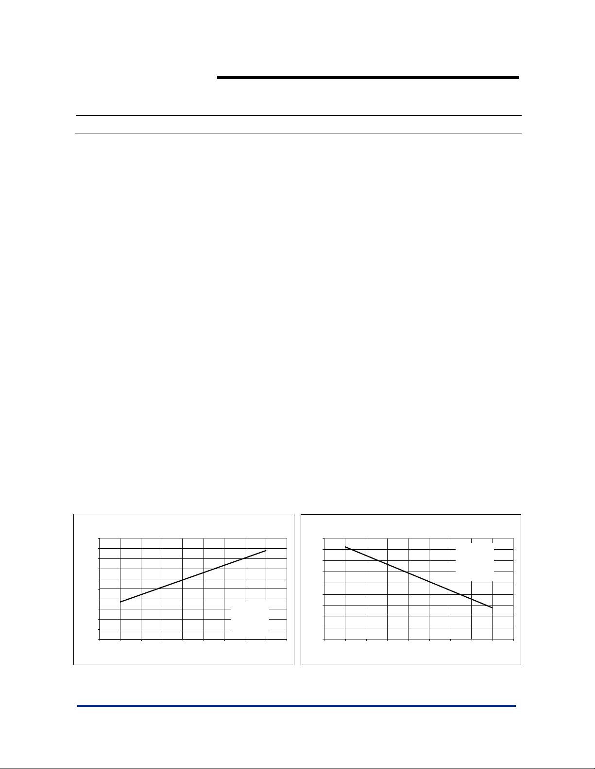
Turn-On Time vs Input Vol tage
750
700
650
600
550
500
450
400
Turn-On Time (us)
350
300
250
1.5 2 2.5 3 3.5 4 4.5 5 5.5 6
Input Voltage (V)
CL=1uF
RL=10
TA=25°C
Iout
500mA/div
10ms/div
Channel 1 Disabled and Channel 2 Enabled
Ven1
5V/div
Vout 1
5V/div
Ven2
5V/div
Vout 2
5V/div
50ms/div
Turn-Off Tim e v s Input Volt a ge
30
29
29
28
28
27
27
Turn-Off Time (us)
26
26
25
1.5 2 2.5 3 3.5 4 4.5 5 5.5 6
Input Voltage (V)
CL=1uF
RL=10
TA=25°C
TA=25°C
CL=68uF
AP2162/AP2172 Rev. 5
www.diodes.com © Diodes Incorporated
10 of 17 FEBRUARY 2009
Page 11

1A DUAL CHANNEL CURRENT-LIMIT ED POWER
Typical Performance Characteristics (Continued)
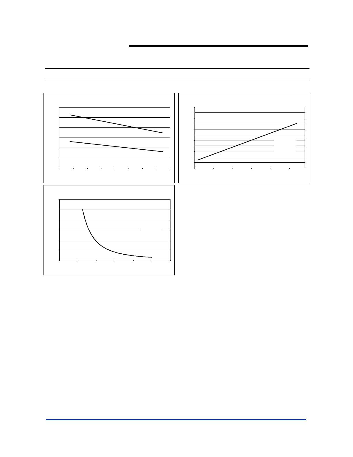
Rise Time vs Input Voltage
650
600
550
500
450
400
Rise Time (us)
350
300
250
22.533.544.555.56
Input Voltage (V)
CL=1uF
RL=10
=
°
22
22
21
21
Fall Time (us)
20
20
19
22.533.544.555.56
AP2162/AP2172
SWITCH
Fall Time vs I nput Voltage
CL=1uF
RL=10
=
°
Input Voltage (V)
Supply Current, Out put Enabled vs Ambient Te m per a t ur e
68
63
58
Vin=5.5V
53
48
43
38
33
Supply Current, Output Enabled (uA)
28
-60 -40 -20 0 20 40 60 80 100
Static Dra i n- Sour ce On-State Resistance vs Am bient
170
160
150
140
130
120
110
Resistance (mΩ)
100
Static Drain-Source On-State
90
80
-60 -40 -20 0 20 40 60 80 100
Vin=5.0V
A mbient Temperature (°C)
Temperature
Vin=2.7V
Ambient Temperature (° C)
Vin=3.3V
Vin=2.7V
Vin=3.3V
Vin=5V
Supply Curr e nt , Outpu t Disabled vs Ambie nt T em pe r a t ure
0.8
0.7
0.6
0.5
0.4
0.3
0.2
0.1
Supply Current, Output Disabled (uA)
0.0
-60 -40 -20 0 20 40 60 80 100
1.56
1.55
1.54
1.53
1.52
1.51
1.50
1.49
1.48
1.47
Short-Circuit Output Current (A)
1.46
1.45
Vin=3.3V
Short- Circui t Outp ut Current vs Am b ient Tem p erature
CL=100uF
Vin=2.7V
-60 -40 -20 0 20 40 60 80 100
Vin=5.0V
Vin=2.7V
Ambient Temperature (° C)
Ambient Temperature (°C)
Vin=5.5V
Vin=3.3V
Vin=5.0V
Vin=5.5V
AP2162/AP2172 Rev. 5
www.diodes.com © Diodes Incorporated
11 of 17 FEBRUARY 2009
Page 12
1A DUAL CHANNEL CURRENT-LIMIT ED POWER
Typical Performance Characteristics (Continued)
Undervoltage Lockout vs Ambien t T em pe r a ture
2.20
2.10
2.00
1.90
1.80
Undervoltage Lockout (V)
1.70
1.60
-60 -40 -20 0 20 40 60 80 100
UVLO Rising
UVLO Falling
Ambient Tem perature (°C)
1.99
1.98
1.97
1.96
1.95
1.94
1.93
1.92
1.91
Threshold Trip Current (A)
1.90
1.89
1.88
2.83.33.84.34.85.3
AP2162/AP2172
Threshold Tri p Curr e nt vs I nput Voltage
Input Voltage (V)
SWITCH
TA=25°C
CL=68uF
Current Limit Response vs Peak Current
120
100
80
60
40
Current Limit Response (us)
20
0
024681012
Peak Current (A)
VIN=5V
=25°C
T
A
=68uF
C
L
AP2162/AP2172 Rev. 5
www.diodes.com © Diodes Incorporated
12 of 17 FEBRUARY 2009
Page 13

AP2162/AP2172
1A DUAL CHANNEL CURRENT-LIMIT ED POWER
SWITCH
Application Note
Power Supply Considerations
A 0.01-F to 0.1-F X7R or X5R ceramic bypass capacitor between IN and GND, close to the device, is
recommended. Placing a high-value electrolytic capacitor on the input and output pin(s) is recommended
when the output load is heavy. This precaution reduces power-supply transients that may cause ringing on
the input. Additionally, bypassing the output with a 0.01-F to 0.1-F ceramic capacitor improves the
immunity of the device to short-circuit transients.
Over-current and Short Circuit Protection
An internal sensing FET is employed to check for over-current conditions. Unlike current-sense resistors,
sense FETs do not increase the series resistance of the current path. When an overcurrent condition is
detected, the device maintains a constant output current and reduces the output voltage accordingly.
Complete shutdown occurs only if the fault stays long enough to activate thermal limiting.
Three possible overload conditions can occur. In the first condition, the output has been shorted to
GND before the device is enabled or before V
circuit and immediately clamps output current to a certain safe level namely I
In the second condition, an output short or an overload occurs while the device is enabled. At the instance
the overload occurs, higher current may flow for a very short period of time before the current limit function
can react. After the current limit function has tripped (reached the over-current trip threshold), the device
switches into current limiting mode and the current is clamped at I
In the third condition, the load has been gradually increased beyond the recommended operating current.
The current is permitted to rise until the current-limit threshold (I
the device is exceeded. The AP2162/AP2172 is capable of delivering current up to the current-limit threshold
without damaging the device. Once the threshold has been reached, the device switches into its current
limiting mode and is set at I
LIMIT
.
FLG Response
When an over-current or over-temperature shutdown condition is encountered, the FLG open-drain output
goes active low after a nominal 7-ms deglitch timeout. The FLG output remains low until both over-current
and over-temperature conditions are removed. Connecting a heavy capacitive load to the output of the
device can cause a momentary over-current condition, which does not trigger the FLG due to the 7-ms
deglitch timeout. The AP2162/AP2172 is designed to eliminate false over-current reporting without the need
of external components to remove unwanted pulses.
Power Dissipation and Junction Temperature
The low on-resistance of the internal MOSFET allows the small surface-mount packages to pass large
current. Using the maximum operating ambient temperature (T
calculated by:
D = RDS(ON)× I
P
Finally, calculate the junction tem perature:
J = PD x RθJA + TA
T
Where:
T
A= Ambient temperature °C
θJA = Thermal resistance
R
P
D = Total power dissipation
2
IN has been applied. The AP2162/AP2172 senses the short
.
LIMIT
.
LIMIT
) is reached or unti l the thermal limit of
TRIG
A) and RDS(ON), the power diss ipation can be
AP2162/AP2172 Rev. 5
www.diodes.com © Diodes Incorporated
13 of 17 FEBRUARY 2009
Page 14

AP2162/AP2172
1A DUAL CHANNEL CURRENT-LIMIT ED POWER
SWITCH
Application Note (Continued)
Thermal Protection
Thermal prot ection pr events th e IC from dama ge when heav y-overlo ad or short -circuit faults ar e present f or
extended periods of time. The AP2162/AP2172 implements a thermal sensing to monitor the operating
junction temperature of the power distribution switch. Once the die tempe rat u r e ri se s to appr o x ima te ly 14 0° C
due to excessive power dissipation in an over-current or short-circuit condition the internal thermal sense
circuitry turns the power switch off, thus preventing the power switch from damage. Hysteresis is built into
the thermal sense circuit allowing the device to cool down approximately 25°C before the switch turns back
on. The switch continues to cycle in this manner until the load fault or input power is removed. The
FLG open-drain output is asserted when an over-temperature shutdown or over-current occurs with 7-ms
deglitch.
Under-voltage Lockout (UVLO)
Under-voltage lockout function (UVLO) keeps the internal power switch from being turned on until the power
supply has reached at least 1.9V, even if the switch is enabled. Whenever the input voltage falls below
approximately 1.9V, the power switch is quickly turned off. This facilitates the design of hot-insertion systems
where it is not possible to turn off the power switch before input power is removed.
Host/Self-Powered HUBs
Hosts and self-powered hubs (SPH) have a local power supply that powers the embedded functions and the
downstream ports (see Figure 2). This power supply must provide from 5.25V to 4.75V to the board side of
the downstream connection under both full-load and no-load conditions. Hosts and SPHs are required to
have current-limit protection and must report over-current conditions to the USB controller. Typical SPHs are
desktop PCs, monitors, printers, and stand-alone hubs.
Figure 2. Typical Two-Po rt U S B Host / Self-Powered Hub
Generic Hot-Plug Applications
In many applications it may be necessary to remove modules or pc boards while the main unit is still
operating. These are considered hot-plug applications. Such implementations require the control of current
surges seen by the main power supply and the card being inserted. The most effective way to control these
surges is to limit and slowly ramp the current and voltage being applied to the card, similar to the way in
which a power supply normally turns on. Due to the controlled rise times and fall times of the
AP2162/AP2172, these devices can be used to provide a softer start-up to devices being hot-plugged into a
powered syst em. The UV LO feat ure of the AP 2162/A P2172 al so ensur es that the switc h is off aft er the car d
has been removed, and that the switch is off during the next insertion.
By placing the AP2162/AP2172 between the VCC input and the res t of the cir cuitry, t he input powe r reaches
these devices first after insertion. The typical rise time of the switch is approximately 1ms, providing a slow
voltage ramp at the output of the device. This implementation controls system surge current and provides a
hot-plugging mechanism for any device.
AP2162/AP2172 Rev. 5
14 of 17 FEBRUARY 2009
www.diodes.com © Diodes Incorporated
Page 15

Marking Information
(1) SOP-8L
AP2162/AP2172
1A DUAL CHANNEL CURRENT-LIMIT ED POWER
SWITCH
( Top view )
8765
Part Number
6 : Active Low
7 : Active High
(2) MSOP-8L-EP
Part Number
6 : Active Low
7 : Active High
Logo
Logo
AP21X X
YY WW X X
2
1
( Top view )
8765
34
Y
W X E
AP21X X
234
1
2 : 2 Channel
G : Green
YY
: Year : 08, 09,10~
: Week : 01~52; 52
WW
represents 52 and 53 week
X
: Internal Code
A~Z : Green
MSOP-8L-EP
Y
: Year : 0~9
: Week : A~Z : 1~26 week;
W
a~z : 27~52 week; z represents
52 and 53 week
2 : 2 Channel
AP2162/AP2172 Rev. 5
www.diodes.com © Diodes Incorporated
15 of 17 FEBRUARY 2009
Page 16

1A DUAL CHANNEL CURRENT-LIMIT ED POWER
Package Information ( All Dimensions in mm )
(1) Package type: SOP-8L
0.254
3.85/3.95
5.90/6.10
0.10/0.20
Detail "A"
0.62/0.82
Gauge Plane
Seating Plane
AP2162/AP2172
SWITCH
7°~9°
1.27typ
8x-0.60
6x-1.27
8x-1.55
Land Pattern Recommendation
0.3/0.5
4.85/4.95
5.4
(Unit: mm)
(2) Package type: MSOP-8L-EP
2.9/3.1
1
0.65Bsc.
0.22/0.38
0.75/0.95
0.35max.
0.15/0.25
1.30/1.50
1.75max.
8x-0.45
4.7/5.1
8x-1.4
Land Pattern Recommendation
0.15Typ.
(Unit:mm)
1.10Max.
6x-0.65
45°
EXPOSED PAD
4.4
1
7°~9°
(BOTTOM)
"A"
Detail "A"
0°/8°
0.05
2.9/3.1
1
1.65/1.95
EXPOSED PAD
(BOTTOM)
1.35/1.65
0.4/0.8
0.05/0.15
DETAIL "A"
0.95Ref.
AP2162/AP2172 Rev. 5
www.diodes.com © Diodes Incorporated
0.25
Gauge plane
°
8
/
°
0
16 of 17 FEBRUARY 2009
Page 17

AP2162/AP2172
1A DUAL CHANNEL CURRENT-LIMIT ED POWER
SWITCH
IMPORTANT NOTICE
Diodes Incorporated and its subsidiaries reserve the right to make modifications, enhancements, improvements, corrections or other changes without further
notice to any product herein. Diodes Incorporated does not assume any liability arising out of the application or use of any product described herein; neither
does it convey any license under its patent rights, nor the rights of others. The user of products in such applications shall assume all risks of such use and will
agree to hold Diodes Incorporated and all the companies whose products are represented on our website, harmless against all damages.
LIFE SUPPORT
Diodes Incorporated products are not authorized for use as critical components in life support devices or systems without the expressed written approval of the
President of Diodes Incorporated.
AP2162/AP2172 Rev. 5
www.diodes.com © Diodes Incorporated
17 of 17 FEBRUARY 2009
 Loading...