

Page 1
SERVICE MANUAL
For Europe & U.K. model
Version 2
MODEL
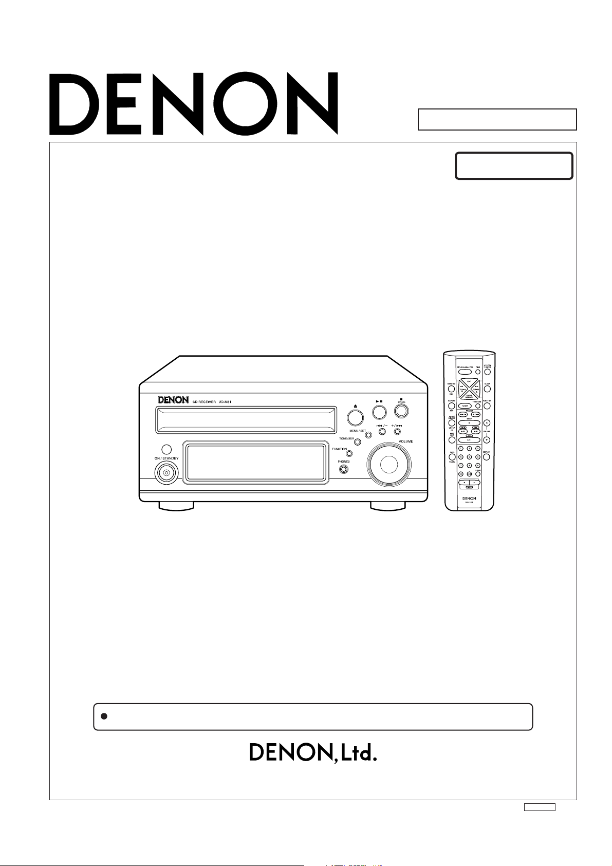
STEREO CD RECEIVER
UD-M31
Some illustrations using in this service manual are slightly different from the actual set.
16-11, YUSHIMA 3-CHOME, BUNKYOU-KU, TOKYO 113-0034 JAPAN
Telephone: 03 (3837) 5321
X0164V.02 DE/CDM 0302
Page 2
SAFETY PRECAUTIONS
The following check should be performed for the continued protection of the customer and service technician.
LEAKAGE CURRENT CHECK
Before returning the unit to the customer, make sure you make either (1) a leakage current check or (2) a line to chassis
resistance check. If the leakage current exceeds 0.5 milliamps, or if the resistance from chassis to either side of the
power cord is less than 460 kohms, the unit is defective.
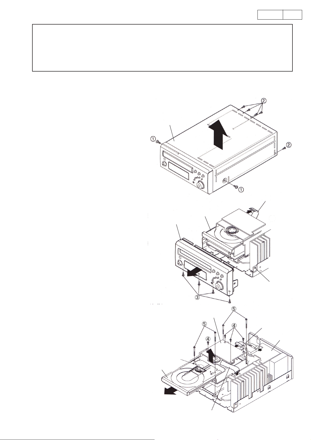
DISASSEMBLY
(Follow the procedure below in reverse order when reassembling)
1. TOP COVER
(1) Remove 2screws ① on both sides.
(2) Remove 5screws ② on the rear.
(3) Detach the Top Cover to the arrow direction.
Top cover
2UD-M31
2. FRONT PANEL
(1) Disconnect FFC on thr rear of the CD
Mecha.
(2) Remove 4 lower screws ③
(3) Detach the Front Panel with releasing the
hooks on both sides.
3. CD MECHANISM UNIT
(1) Disconnect FFC coming from the top of the
CD Mecha.
(2) Unplug the connector on fhe rear of the
µcom PWB .
(3) Unplug the connector on the I/O PWB.
(4) Remove 4 screws ④ on the µcom PWB .
(5) Fully pull out the loader by turning the gear
under the loader of the CD Mecha.
(6) Remove 4 screws ⑤ to detach the CD
Mecha.
FFC
CD Mecha.
Front Panel
Hook
µcon P.W.B.
Connector
I/O P.W.B.
Gear
Loader
FFC
2
Page 3
3UD-M31
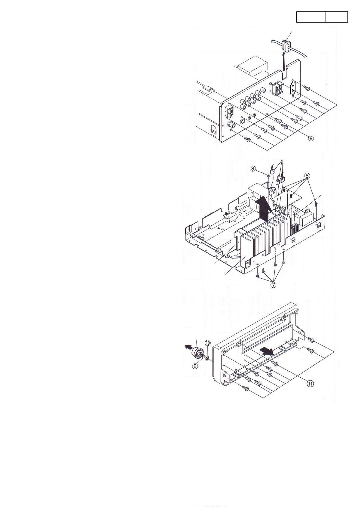
4. REAR PANEL
(1) Pull out the cord bush.
(2) Remove 12 screws ⑥
5. MAIN PWB
(1) Remove 4 screws ⑦ fixing the radiator the chas-
sis.
(2) Unplug 3 connectors on the AMP PWB.
(3) Detach the Main PWB together with the radiator .
(4) Remove 5 screws ⑧ .
(5) Detach the Power PWB.
Cord Bush
Connector
Power
P.W.B.
6. DISPLAY PWB
(1) Pull out the VR knob.
(2) Remove the spacer and the VR nut ⑨ .
(3) Remove 7 screws ⑩ .
Main P.W.B.
Radiator
VR knob
3
Page 4
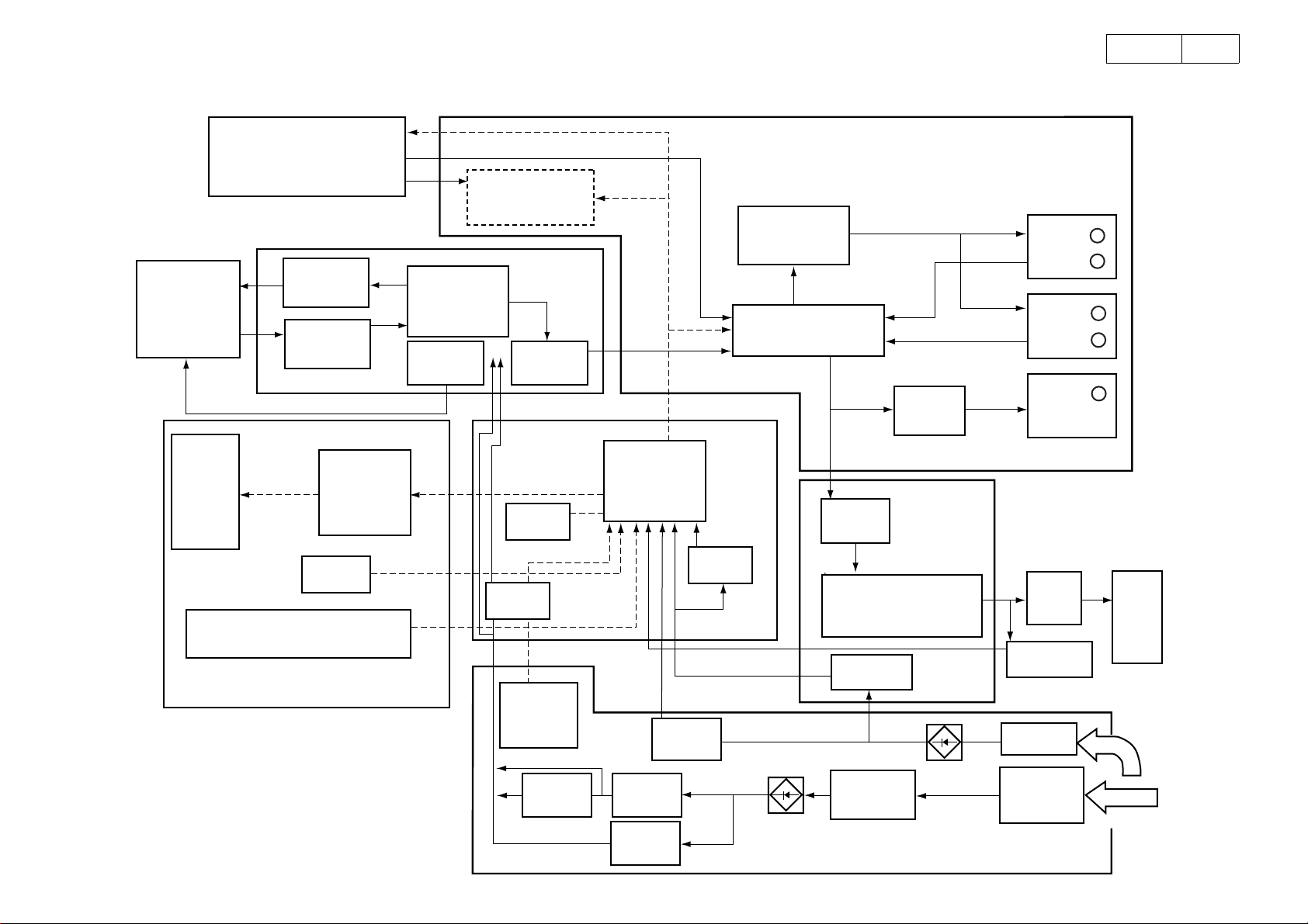
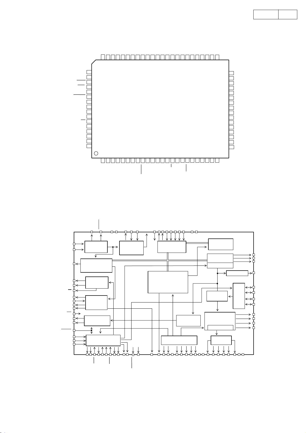
BLOCK DIAGRAM
TUNER MODULE
CD
MECHA
CD11FTA3N
FL401
FL TUBE
IC801
LA6559
DRIVER
IC802
LA9241
RF AMP
LC75725E
FL DRIVER
IC401
IC803
LC78625E
CD DSP
IC805
BA6287F
IC303
LC72720NM
RDS(E2/EK only)
IC804
BA4510F
IC202
93LC66
IC201
UPD784216
MICON
IC301
BU4066BCF
REC OUT SEL
IC302
LC75432M
SELECTOR & VR & EQ
IC304
BA15218F
IC305
BA15218F
REC out
IN
REC out
IN
Pre out
UD-M31
4
IC402
RPM6938
TACT SW & VR ENCORDER
IC203
BA05ST
DENON
BUS
TR601∼603
IC602
NJM
7805FA
P.DOWM
IC603
NJM
7812FA
IC604
NJM
7806FA
TR607
4
IC205
M51957
IC501
STK402-050
POWER AMP
IC605
NJM7805F
POWER
TRANS
RL601
SP
RELAY
Protection
TR501∼
SUB
TRANS
RL602
POWER
RELAY
SP
OUT
AC IN
Page 5
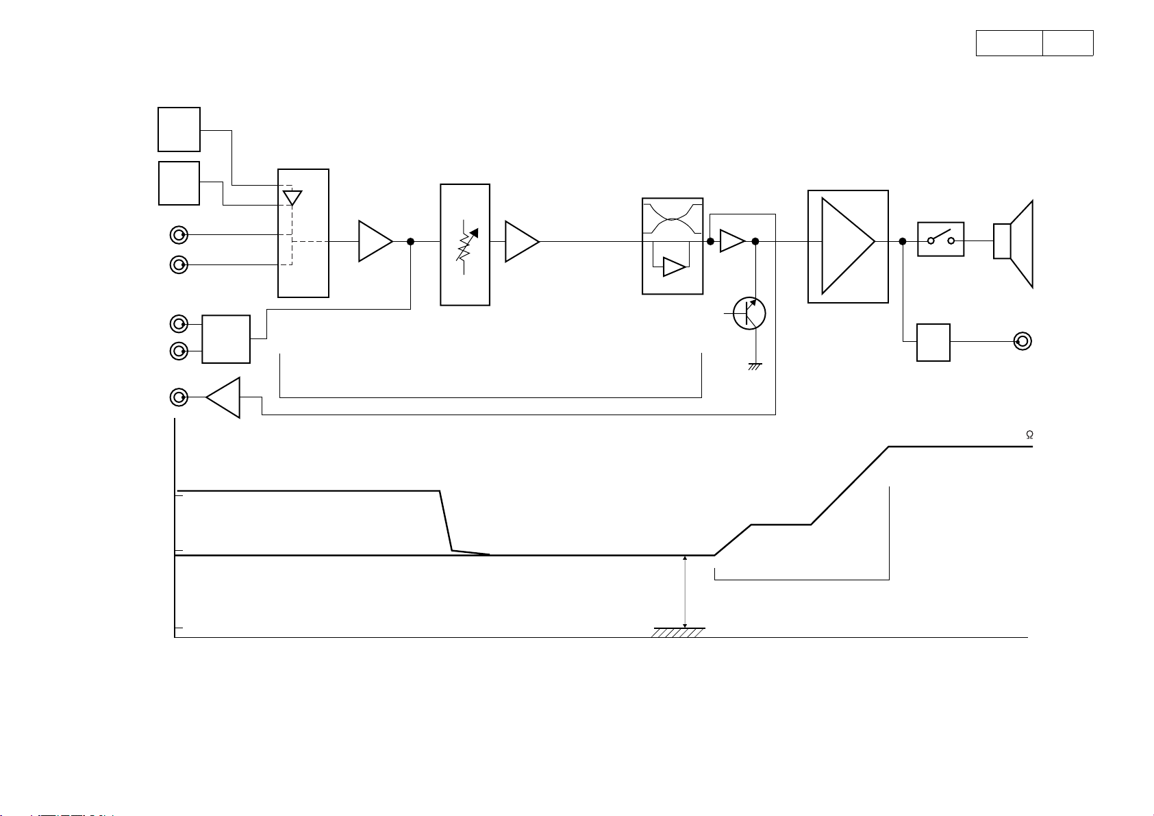
LEVEL DIAGRAM
0dB=0.55V
CD
UNIT
UD-M31
5
LINE 1
LINE 2
LINE 1
REC
LINE 2
REC
PRE OUT
-10dB
TU
UNIT
ANALOG
SWITCH 4066
(dBV)
+16dB
0dB play back CD=1.1V
0dB
LINE:1kHZ,150mV
EQ:FLAT
SDB:OFF
FUNCTION SWITCH
+4dB
+0.83dB
MASTER VOLUME
BUFFER BUFFER
LC75342M
MUTE
-16.4dB
(+6dB)
TOTAL 36dB
POWER AMPTONE/SDB
RELAY SP
ATT
(+30dB)
HP
15W/6
9.49V
-104dB
87.6dB
5
Page 6
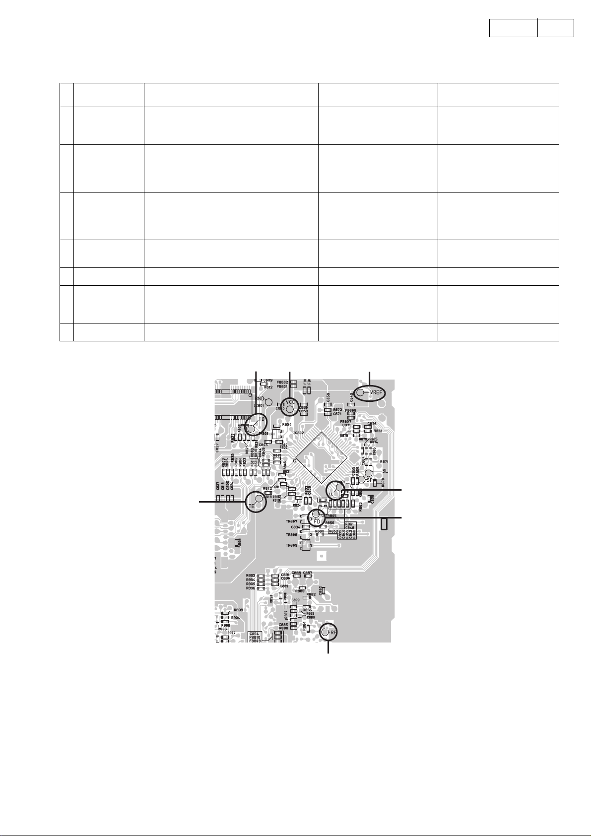
CD TEST MODE
Setting of the test mode and explanation of each button
ITEM OPERATION FUNCTION DISPLAY
6UD-M31
1 Start the mode
2 Disc load
Focus and Track-
3
ing check mode
4 Move pick up
5 Stop move Push the STOP button Stop the movement 1.Display "01"
6 All Servo on Push the SKIP button All servo on, and auto adjust
7 Clear this mode Unplug the AC cord
Plug the AC cord to the wall outlet while pushing the POWER button and the Function button
1.Push the OPEN/CLOSE button and the
LOADER open
2.Place the disc and push the OPEN/CLOSE
button again
1.Push the PLAY button
2.Push the PLAY button again
3.Push the PLAY button again
1.Push the SKIP forward button or the SKIP
reverse button while stopping
TD
VCC VREF
1.This service mode starts
2.Pick up moves to the 10mm
position.
1.Load the CD disc
2.The pick up moves to the
10mm position
1.The laser ON
2.forcus servo on,the disc turns
3.Tracking servo and Slide
servo on
The pick up move forward or
reverse
1.Display "01"
2.The PLAY and the PAUSE
mark lit
1.Display "01"
2.The PLAY and the PAUSE
mark lit
1.Display "02 L on"
2.Display"03 Fon"
3.Display "04 t on"
1.Display "5 O PU"
1.Display "06 Adj."
1.after auto adjust,d
display "01"
FE
TE
FD
1U-3507
CD UNIT
RF
* Laser light of the pickup is always emitted regardless of DISC loading in the test mode.
You may lose your eyesight if you look into the laser directly.
So be careful enough when operating in the test mode.
6
Page 7
How to check the test mode
( 1 ) DISC discrimination, adjustment
* Insert DISC, and press the AUTO SEARCH REVERSE button.
* “06 Adj” is displayed, and discrimination of DISC size 8 cm/12 cm, discrimination of DISC reflectance (CD, CD-
R/CD-RW), adjustment of focus, tracking offset, and EF balance will be performed. (Adjusted values are not
displayed: Refer to Fig. 2, 3)
7UD-M31
FE
TE
RI
FE
TB
SLD
DRF
Fig. 2 DISC discrimination,
Fig. 3 Adjustment of EF balance
adjustment (Case of CD-RW)
* After completing the discrimination and adjustment, it becomes stop condition.
* Once discrimination of DISC has been carried out in the “06 Adj” mode, discrimination of size and reflectance is
no longer made, and only adjustment will be performed.
( 2 ) Checking of servo state
* Press the PLAY button after performing above (1) “DISC discrimination, adjustment”.
* “02 L on” is displayed, and the laser will start to light. (The pickup may vibrate with a rattling noise if DISC has
been loaded, but this is not abnormal.)
* Press the PLAY button again.
* “03 F on” is displayed. DISC starts turning, and focus servo will be actuated. (Refer to Fig. 4, 5)
FE
TE
TE
RF
Fig. 4 In “03 F on” Fig. 5 In “03 F on”
* Press the PLAY button again.
* “04 t on” is displayed. Tracking, CLV, and slide servo will be actuated.
* Monitor HF signal using the Test Point, HF point and VC point.
Check that the signal’s amplitude is 1.5V±0.3Vp-p. (Refer to Fig. 6)
RF
A (A=1.5±0.3Vp-p)
Fig. 6 In “04 t on”
7
Page 8
WAVE-FORMS OF EACH POINT
8UD-M31
SP
SP
FE
TE
DRF
RF
When 12 cm DISC
start
When 8 cm DISC
start
When focus
servo on
SP
SP
TD
TE
RF
DRF
When 12 cm DISC
stop
When 8 cm DISC
stop
During PAUSE
SL
TE
SL
OPEN
CLOSE
Track search
(when forward)
During PLAY
When the tray
OPEN
SL
TE
FD
Track search
(when reverse)
Focus search
(no DISC)
8
Page 9
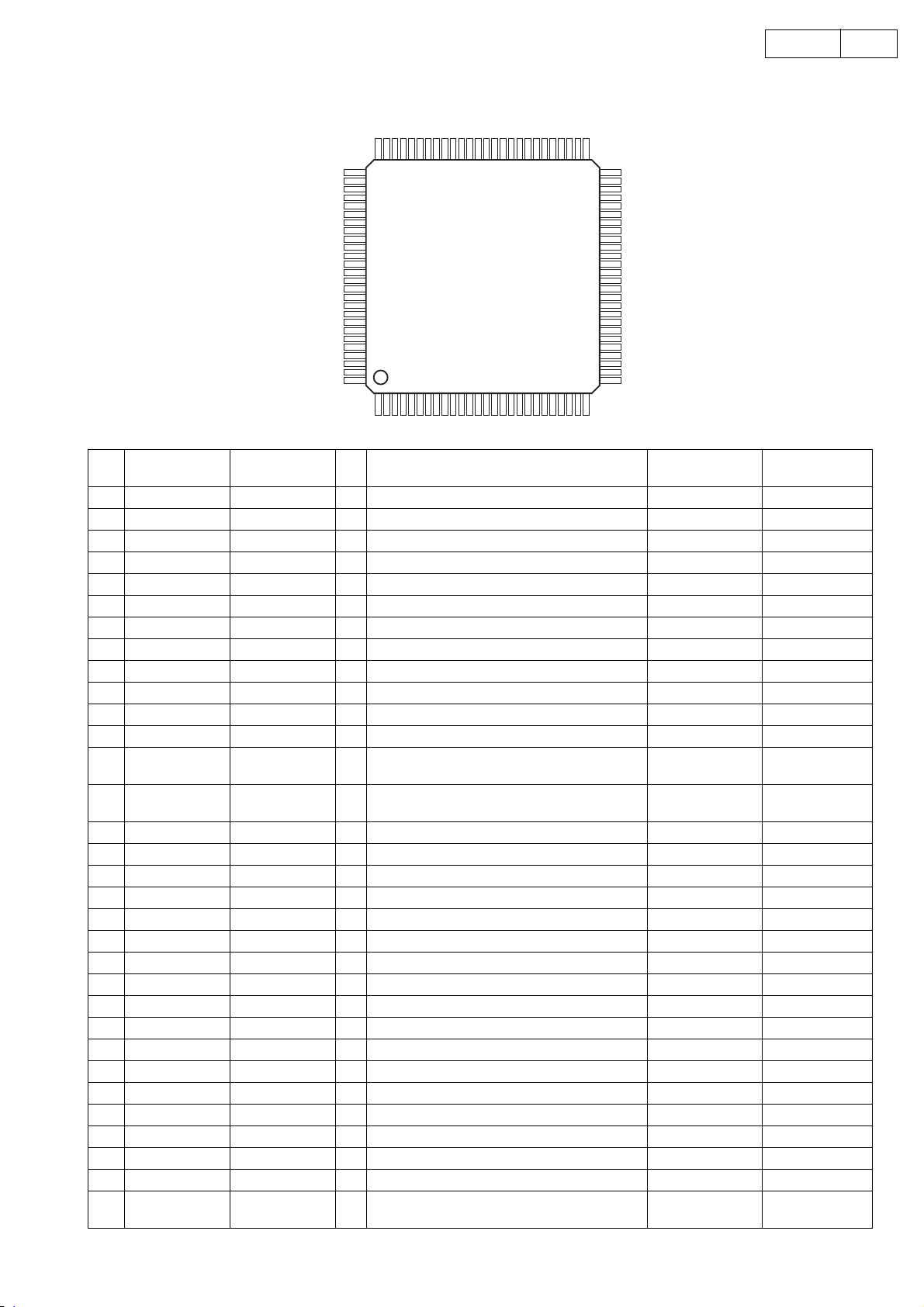
SEMICONDUCTOR
IC’s µPD784216AGC-8EU(IC201)
76
75
9UD-M31
51
50
100
1
26
25
µPD784216AGC-8EU Terminal Function
Pin
No.
1 P120/RTP0 ENC A I Rotary encoder INPUT A RECIEVER -
2 P121/RTP1 ENC B I Rotary encoder INPUT B RECIEVER -
3 P122/RTP2 V.MUTE O Volume mute output, mute;High RECIEVER H
4 P123/RTP3 POWER O Amp circuit power ON/OFF output, ON:High RECIEVER L
5 P124/RTP4 /R.MUTE O Speaker Relay ON/OFF output, ON:High RECIEVER L
6 P125/RTP5 NC O Not used :NC OTHER L
7 P126/RTP6 SEL.EEPROM O EEPROM chip enable output RECIEVER L
8 P127/RTP7 FLCE O Chip select output to FL tube controller OTHER L
9 VDD VDD - Positive power OTHER -
10 X2 X2 - X'tal connection for main clock oscillation OTHER -
11 X1 X1 I X'tal connection for main clock oscillation OTHER -
12 VSS VSS - GND potential OTHER -
13 XT2 XT2 - x'tal connection for main sub-clock oscillation,
14 XT1 XT1 I x'tal connection for main sub-clock oscillation,
15 /RESET /RESET I Micro-computer reset input OTHER -
16 P00/INTP0 REMOCON I Remote-control receive data input RECIEVER -
17 P01/INTP1 50/60 I 50/60Hz AC input RECIEVER -
18 P02/INTP2/NMI /DB RXD I DENON BUS Data input (interrupt input) RECIEVER -
19 P03/INTP3 PROTECT I Speaker Terminal DC voltage detect signal input RECIEVER -
20 P04/INTP4 SEL.EEPROM O EEPROM chip enable output RECIEVER L
21 P05/INTP5 WRQ I SUB CODE Q STAND BY CD L
22 P06/INTP6 /INT I NC, connect to grand OTHER -
23 AVDD AVDD - A/D converter analog power OTHER -
24 AVref0 Avref0 - A/D converter reference voltage input OTHER -
25 P10/ANI0 KEY1 I Unit operation button input1 RECIEVER -
26 P11/ANI1 KEY2 I Unit operation button input2 RECIEVER -
27 P12/ANI2 KEY3 I Not used :Connect to GND OTHER -
28 P13/ANI3 KEY4 I Not used :Connect to GND OTHER -
29 P14/ANI4 NC I Not used :Connect to GND OTHER -
30 P15/ANI5 DRF I REFLECTION OF DISC SIG. Input CD -
31 P16/ANI6 FSEQ I EFM SYNC SIG. INPUT CD -
32 P17/ANI7 DARXD I DATA BUS(for VOL,PLL,RDS IC, EEPROM)
Port Symbol I/O Function RECIEVER or CD
not used : :NC
not used :Connect to VSS orVCC
-
Data in
outputs of
standby&Defoult
9
Page 10

10UD-M31
Pin
No.
33 AVSS AVSS - A/D,D/A converter GND position OTHER -
34 P130/ANO0 LINE1 O LINE OUT Control signal output1 OTHER L
35 P131/ANO1 LINE2 O LINE OUT Control signal output2 OTHER L
36 AVref1 Avref1 - D/A converter reference voltage input OTHER -
37 P70/RxD2/SI2 SQOUT I Sub Q code data input CD L
38 P71/TxD2/SO2 COIN O CD-DSP serial communication data output CD L
39 P72/ASCK2/
40 P20/RxD1/SI1 NC I Pull up RECIEVER -
41 P21/TxD1/SO1 FLDT O DATA BUS for FL driver, Data output RECIEVER L
42 P22/ACSK1/
43 P23/PCL NC I Pull up RECIEVER -
44 P24/BUZ /RDSRST O RDS IC reset output RECIEVER -
45 P25/SI0/SDA0 DB RXD I DATA BUS for DENON BUS Data input RECIEVER -
46 P26/SO0 DB TXD O DATA BUS for DEON BUS Data output RECIEVER L
47 P27/SCK0/SCL0 DB CLK O DENON BUS Clock output RECIEVER L
48 P80/A0 /SD I FM/AM Tuning signal input, Tuned:Low RECIEVER -
49 P81/AÇP /ST INC I FM stereo demodulation detect input, Ste-
50 P82/A2 /TMUTE O Tuner mute output, mute:Low RECIEVER L
51 P83/A3 AUTO/MONO O FM AUTO/MONO switching, MONO:High RECIEVER L
52 P84/A4 USA I Initial setting input RECIEVER -
53 P85/A5 EURO I Initial setting input RECIEVER -
54 P86/A6 FREQ I Initial setting input RECIEVER -
55 P87/A7 RDS I Initial setting input RECIEVER -
56 P40/AD0 SL+ O SLIDE kick Forward CD L
57 P41/AD1 SL- O SLIDE kick Reverse CD L
58 P42/AD2 CD/!RW O CD, CD-RW gain switching CD L
59 P43/AD3 SERACH O SEARCH control CD L
60 P44/AD4 NC O OPEN CD L
61 P45/AD5 NC O OPEN CD L
62 P46/AD6 LED POWER G O POWER/STANDBY Green LED out-
63 P47/AD7 LED POWER R O POWER/STANDBY Red LED output,Light:High
64 P50/A8 NC I Pull up CD -
65 P51/A9 NC I Pull up CD -
66 P52/A10 CLSW I LOADER CLOSE SW input CD -
67 P53/A11 OPSW I LOADER OPEN SW input CD -
68 P54/A12 NC I Pull up CD -
69 P55/A13 NC I Pull up CD -
70 P56/A14 NC I Pull up CD -
71 P57/A15 O Not used :NC OTHER L
72 VSS VSS - GND potential OTHER -
73 P60/A16 BLK O FLD ON/OFF control port, L= black out FLD
74 P61/A17 DATXD O DATA BUS(for VOL,PLL,RDS IC, EEPROM)
75 P62/A18 DACLK O DATA BUS(for VOL,PLL,RDS IC, EEPROM)
76 P63/A19 DACE O DATA BUS(for VOL,PLL,RDS IC) Chip enable
77 P64/RD DRP_RST O CD-DSP reset output, output, reset:High CD L
78 P65/WR O Not used :NC OTHER L
79 P66/WAIT PWBCHK I Start PWB check mode OTHER -
Port Symbol I/O Function RECIEVER or CD
CQCK O CD-DSP serial communication clock output CD L
SCK2
FLCLK O DATA BUS for FL driver, Clock output RECIEVER L
SCK1
RECIEVER -
reo:Low
put,Light:High
RECIEVER L
Data output
RECIEVER L
Clock output
RECIEVER L
output
outputs of
standby&Defoult
10
Page 11

11UD-M31
Pin
No.
80 P67/ASTB O Not used :NC OTHER L
81 VDD VDD - Positive power OTHER -
82 P100/TI5/TO5 OPEN O CD mecha. Open CD L
83 P101/TI6/TO6 CLOSE O CD mecha. Close CD L
84 P102/TI7/TO7 O NC OTHER L
85 P103/TI8/TO8 O NC OTHER L
86 P30/TO0 RWC O CD-DSP serial communication read / write CD L
87 P31/TO1 O Not used :NC OTHER L
88 P32/TO2 DRV_MUTE O DRIVER MUTE CD L
89 P33/TI1 O Not used :NC, CD L
90 P34/TI2 CDPOWER O CD power control signal output CD L
91 P35/TI00 O Not used :NC, OTHER L
92 P36/TI02 O Not used :NC OTHER L
93 P37 HPSW I HEADPHONE Insertswitch detective signal input
94 TEST/VPP TEST I not used :Connect to GND OTHER -
95 P90 O Not used :NC, OTHER L
96 P91 OPSW I Pickup inner-most detect input, inner most:Low
97 P92 O Not used :NC OTHER L
98 P93 O Not used :NC OTHER L
99 P94 O Not used :NC OTHER L
100 P95 O Not used :NC OTHER L
Port Symbol I/O Function RECIEVER or CD
-
at on
outputs of
standby&Defoult
11
Page 12
LC78625E(IC803)
RWC
WRQ
626364
FSX
SBCK
SFSYPWEFLG
59
58
6061
SBSY
57
56
DOUT
55
MUTER
RVDDRCHP
53
54
RCHN
RVSSLVSSLCHN
50
5152
49
LCHP
48
47
LVDDMUTEL
C2F
45
44
46
12UD-M31
ROMXA
CK2
LRSY
ASLRCK/P3
43
4142
SQOUT
CO IN
CQCK
RES
TST11
LASER
16M
4.2M
CONT
TEST5
CS
XV
XIN
XOUT
XV
TEST1
65
66
67
68
69
70
71
72
73
74
75
76
SS
77
78
79
DD
80
1
23
DEFI
4567
TAI
PDO
FR
ISET
VVSS
VVDD
8
9
VSS
10
EFMO
EFMO
11
EFMIN
12 13
TEST2
17 18 19 20
15 16
14
V/P
FST
FOCS
FZD
CLV-
CLV+
HFL
21
TES
22
PCK
FSEQ
23 24
TOFF
TGL
40
ASDEPC/P2
39
ASDFIN/P1
38
ASDACK/P0
37
TST10
36
DACKO
35
DFOLO
34
DFORO
33
LRCKO
32
EMPH
31
TEST4
30
DEMO
29
JP-
28
JP+
27
V
DD
26
TEST3
25
THLD
DEFI
EFMIN
FSEQ
CLV+
CLV-
V/P
PW
SBCK
SBSY
SFSY
CS
WRQ
SQOUT
CQCK
CO IN
RWC
DEMO
EFMO
EFMO
Slice Level
Control
Synchronization
detection
EFM Demodulation
CLV
Digital servo
Subcode
separation
Q CRC
Microprocessor
Interface
Servo
commander
FST
HFL
FZD
TOFF
FOCS
TES
DD
RES
VVSSVV
JP+
PDO
ISET
VCO
oscillator
Clock control
JP-
TGL
THLD
PCK
FR
detection and correction
CONT
LASER
EMPH
TST11
TST10
TAI
2k
TEST1
´
RAM
TEST2
8-bit
TEST3
C1 and C2 error
Flag processing
Crystal oscillator system
Timing generator
SS
16M
XV
4.2M
EFLG
TEST5
TEST4
Level meter
Peak meter
XIN
FSX
XOUT
DD
XV
DD
VSSV
CK2
RAM address
generator
Interpolation
and mute
Bilingual function (1)
Digital
attenuator
8´ oversampling
digital filters
Bilingual function (2)
One-bit D/A
converter
SS
DD
RV
RV
RCHP
MUTER
Digital output
LCHN
RCHN
LCHP
interface
ports/Anti-shock
General-purpose
SS
DD
LV
LV
MUTEL
LRSY
C2F
ROMXA
DOUT
ASDACK/P0
ASDFIN/P1
ASDEPC/P2
ASLRCK/P3
DACKO
DFOLO
DFORO
LRCKO
12
Page 13
LC78625E Terminal Function
Pin No. Symbol I/O Function
1 DEFI I Defect detection signal (DEF) input (This pin must be connected to 0 V if unused.)
2TAII
3 PDO O External VCO control phase comparator output
4
VV
SS
PLL pins
5 ISET AI PDO output current adjustment resistor connection
6
VV
DD
7 FR AI VCO frequency range adjustment
8 VSS Digital system ground. (This pin must be connected to 0 V.)
9EFMOO
10 EFMO O EFM signal output
Slice level control
11 EFMIN I EFM signal input
12 TEST2 I Test input. A pull-down resistor is built in. This pin must be connected to 0 V in normal operation.
+
13
14
CLV
CLV
15 V/P O
O Spindle servo control output. Acceleration when CLV+ is high, deceleration when CLV- is high.
-
O Three-value output is also possible when specified by microprocessor command.
Rough servo/phase control automatic switching monitor output. Outputs a high level during rough servo and a low
level during phase control.
16 FOCS O Focus servo on/off output. Focus servo is on when the output is low.
17 FST O Focus start pulse output. This is an open-drain output.
18 FZD I Focus error zero cross signal input. (This pin must be connected to 0 V if unused.)
19 HFL I Track detection signal input. This is a Schmitt input.
20 TES I Tracking error signal input. This is a Schmitt input
21 PCK O EFM data playback clock monitor. Outputs 4.3218 MHz when the phase is locked.
22 FSEQ O
Synchronization signal detection output. Outputs a high level when the synchronization signal detected from the
EFM signal and the internally generated synchronization signal agree.
23 TOFF O Tracking off output
24 TGL O Tracking gain switching output. Increase the gain when low.
25 THLD O Tracking hold output
26 TEST3 I Test input. A pull-down resistor is built in. (This pin must be connected to 0 V.)
27
28
29
V
JP
JP
DD
+
-
30 DEMO I
Digital system power supply.
Track jump output. A high level output from JP+ indicates acceleration during an outward jump or deceleration dur-
O
ing an inward jump.
A high level output from JP- indicates acceleration during an inward jump or deceleration during an outward
O
jump.Three-value output is also possible when specified by microprocessor command.
Sound output function input used for end product adjustment manufacturing steps. A pull-down resistor is built in.
(This pin must be connected to 0 V.)
31 TEST4 I Test input. A pull-down resistor is built in. (This pin must be connected to 0 V.)
32 EMPH O De-emphasis monitor pin. A high level indicates playback of a de-emphasis disk.
33 LRCKO O
34 DFORO O Right channel data output
35 DFOLO O Left channel data output
Digital filter outputs
36 DACKO O Bit clock output
37 TST10 O Test output. Leave open. (Normally outputs a low level.)
38
39
40
ASDACK
/P0
ASDFIN/
P1
ASDEPC
/P2
When antishock
I/O
mode is not
used,these pins are
I/O Left and right channel data input
used as general purpose I/O ports (P0 to
P3). They must either
I/O
be set to input mode
and connected to 0 V,
41
ASLRCK/
P3
or set to output mode
I/O L/R clock input
and left open, if
unused.
Test input. A pull-down resistor is built in. (This pin must be connected to 0 V in normal
operation.)
Internal VCO ground. (This pin must be connected to 0 V.) PLL pins
Internal VCO power supply.
EFM signal inverted output
Word clock output
Bit clock input
The antishock inputs in antishock
mode.
Sets the built-in de-emphasis filter on or off.(High:
on, low: off)
13UD-M31
13
Page 14
Pin No. Symbol I/O Function
42 LRSY O
43 CK2 O Bit clock output(after reset)
44 ROMXA O Interpolation data output(after reset) ROM data output (during ROMXA mode)
ROMXA application
output signals
L/R clock output
Inverted polarity clock output(during CK2CON
mode)
45 C2F O C2 flag output
46 MUTEL O
47
LV
DD
Left channel mute output
Left channel power supply
48 LCHP O Left channel P output
49 LCHN O Left channel N output
50
51
LV
RV
SS
SS
One-bit D/A converter
signals
Left channel ground. Must be connected to 0 V.
Right channel ground. Must be connected to 0 V.
52 RCHN O Right channel N output
53 RCHP O Right channel P output
54
RV
DD
Right channel power supply
55 MUTER O Right channel mute output
56 DOUT O Digital output
57 SBSY O Subcode block synchronization signal output
58 EFLG O C1, C2, single and double error correction monitor pin
59 PW O Subcode P, Q, R, S, T, U and W output
60 SFSY O Subcode frame synchronization signal output. This signal falls when the subcodes are in the standby state.
61 SBCK I Subcode readout clock input. This is a Schmitt input. (This pin must be connected to 0 V if unused.)
62 FSX O Output for the 7.35 kHz synchronization signal divided from the crystal oscillator
63 WRQ O Subcode Q output standby output
64 RWC I Read/write control input. This is a Schmitt input.
65 SQOUT O Subcode Q output
66 COIN I Command input from the control microprocessor
67 CQCK I
Input for the command input acquisition clock or the SQOUT pin subcode readout clock input. This is a Schmitt
input.
68 RES I Reset input. This pin must be set low briefly after power is first applied.
69 TST11 O Test output. Leave open. (Normally outputs a low level.)
70 LASER O Laser on/off output. Controlled by serial data commands from the control microprocessor.
71 16M O 16.9344 MHz output
72 4.2M O 4.2336 MHz output
73 CONT O Supplementary control output. Controlled by serial data commands from the control microprocessor.
74 TEST5 I Test input. A pull-down resistor is built in. (This pin must be connected to 0 V.)
75 CS I Chip select input. A pull-down resistor is built in. This pin must be connected to 0 V if unused.
76
XV
SS
77 XIN I
78 XOUT O
79
XV
DD
Crystal oscillator ground. Must be connected to 0 V.
Connections for a 16.9344 MHz crystal oscillator
Crystal oscillator power supply
80 TEST1 I Test input. A pull-down resistor is built in. (This pin must be connected to 0 V.)
14UD-M31
Note: All power-supply pins (VDD, VVDD, LVDD, RVDD, and XVDD) must be connected to the same potential.
14
Page 15

LC75725E(IC401)
S23
S22
S21
S20
S19
S18
S17
S16
S15
S14
S13
S12
S11
S10
S9
48 47 46 45 44 43 42 41 40 39 38 37 36 35 34 33
15UD-M31
S24
BLK
VFL
S8
S7
S6
S5
S4
S3
S2
S1
Vss
OSC0
OSC1
V
BLK
CE
CL
49
50
51
52
53
54
55
56
57
58
59
DD
60
61
62
63
64
DI
G11
DIGIT
DRIVER
1 2 3 4 5 6 7 8 9 10111213141516
G11
G10
G9
G8
G7
G6
G5
G4
G3
G2
G1
VFL
G10G2G1
S43
S42
SEGMENT DRIVER
MPX
LATCH
VFL
S43
S42
S41
32
S25
31
S26
S27
30
29
S28
28
S29
27
S30
26
S31
25
S32
24
S33
23
S34
22
S35
21
S36
20
S37
19
S38
18
S39
17
S40
S2
S1
GRID
CONTROL
DIMMER
TIMING
GENERATOR
SHIFT REGISTER
TIMING
GENERATOR
DIVIDER
OSCI
OSCO
CLOCK
GENERATOR
Terminal Function
Pin No. I/O Name Function
1,13 Power supply pin to driver block
2~12 Digit output pin
14~56 Segment output pin
57 power supply pin
58 OSCO Pin for oscillator
59 OSCI Pin for oscillator
60 V
61 BLK Display off input pin
62 CE Input for serial data transfer
63
64
O
O
-
O
I
-
I
I
I
I
FL
V
G1~G11
S1~S43
Vss
DD
CL
DI
Power supply pin to ligic block
CE : Chip enable
CL : Sync clock
DI : Transfer data
DI
CL
ADDRESS
DETECTOR
CE
VSS
DD
V
15
Page 16

LA9241M(IC802)
VCC1
LDS
LDD
BH1
PH1
LF2
VR
REFI
VCC2
FSS
DRFCEDATCLCLK
646362616059585756555453525150
FIN2
1
FIN1
2
E
3
F
4
TB
5
-
TE
6
TE
7
TESI
8
SCI
9
TH
10
TA
11
-
TD
12
TD
13
JP
14
15
TO
16
FD
171819202122232425262728293031
FAFAFE
FD
-
-
FE
AGND
NC
SP
SPG
-
SP
SPD
LA9241M Terminal Function
SLD
SLEQ
16UD-M31
VCC1
LDS
LDD
BH1
DEF
49
1
48
NC
47
TBC
46
FSC
45
DGND
44
SLI
43
SLC
-
42
RFS
41
RFSM
+
40
CV
-
39
CV
38
SLOF
37
HFL
36
TES
35
TOFF
34
TGL
+
33
JP
32
-
-
+
JP
SL
SL
FIN2
FIN1
TESI
2
3
E
4
F
5
TB
6
TE
TE
7
8
9
SCI
10
TH
TA
11
-
TD
12
TD
13
JP
14
TO
15
FD
16
APC
I/V
T. SERVO & T.LOGIC
PH1
RF DET
VCA
VCABAL
TE
F.SERVO & F.LOGIC
17 18 19 20 21 22 23 24 25 26 27 28 29 30 31 32
FA
FD
FAFEFE
LF2VRREFI
REF
INTER FACE
-
AGND
-com
SPINDLE
SERVO
SP
NC
VCC2FSS
SP
SPG
DRFCEDATCLCLK
SLED SERVO
SPD
SLEQ
49505152535455565758596061626364
SLC
RF Amp
SLSLJP
SLD
DEF
NC
48
47
TBC
FSC
46
45
DGND
SLI
44
SLC
43
-
42
RFS
RFSM
41
+
CV
40
-
CV
39
SLOF
38
37
HFL
TES
36
TOFF
35
TGL
34
+
33
JP
-
+
Pin No. Symbol Contents
1FIN2
Pickup photodiode connection pin. Added to FIN1 pin to generate the RF signal, subtracted from FIN1 pin to generate
the FE signal.
2 FIN1 Pickup photodiode connection pin.
3 E Pickup photodiode connection pin. Subtracted from F pin to generate the TE signal.
4 F Pickup photodiode connection pin.
5 TB TE signal DC component input pin.
6
TE
-
Pin which connects the TE signal gain setting resistor between this pin and TE pin.
7 TE TE signal output pin.
8 TESI TES (Track Error Sense) comparator input pin. The TE signal is input through a bandpass filter.
9 SCI Shock detection input pin.
10 TH Tracking gain time constant setting pin.
11 TA TA amplifier output pin.
-
12
TD
Pin for configuring the tracking phase compensation constant between the TD and VR pins.
13 TD Tracking phase compensation setting pin.
14 JP Tracking jump signal (kick pulse) amplitude setting pin.
15 TO Tracking control signal output pin.
16 FD Focusing control signal output pin.
-
17
FD
Pin for configuring the focusing phase compensation constant between the FD and FA pins.
18 FA Pin for configuring the focusing phase compensation constant between the FD- and FA- pins.
19
FA
-
Pin for configuring the focusing phase compensation constant between the FA and FE pins.
20 FE FE signal output pin.
21
FE
-
Pin which connects the FE signal gain setting resistor between this pin and FE pin.
22 AGND Analog signal GND.
23 NC No connection
24 SP CV+ and CV- pins input signal single-end output.
25 SPG 12-cm spindle mode gain setting resistor connection pin.
-
26
SP
Spindle phase compensation constant connection pin, along with the SPD pin.
27 SPD Spindle control signal output pin.
28 SLEQ Sled phase compensation constant connection pin.
29 SLD Sled control signal output pin.
30
31
SL
SL
-
Input pin for sled movement signal from microprocessor.
+
Input pin for sled movement signal from microprocessor.
16
Page 17

Pin No. Symbol Contents
32
33
JP
JP
-
Input pin for tracking jump signal from DSP.
+
Input pin for tracking jump signal from DSP.
34 TGL Input pin for tracking gain control signal from DSP. Gain is low when TGL is high.
35 TOFF Input pin for tracking off control signal from DSP. Tracking servo is off when TOFF is high.
36 TES Output pin for TES signal to DSP.
37 HFL The High Frequency Level is used to determine whether the main beam is positioned over a bit or over the mirrored
38 SLOF Sled servo off control input pin
-
39
40
CV
CV
Input pin for CLV error signal from DSP.
+
Input pin for CLV error signal from DSP.
41 RFSM RF output pin.
42
RFS
-
RF gain setting and EFM signal 3T compensation constant setting pin, along with the RFSM pin.
43 SLC Slice Level Control is an output pin that controls the data slice level used by the DSP for the RF waveform.
44 SLI Input pin used by DSP for controlling the data slice level.
45 DGND Digital system GND pin.
46 FSC Focus search smoothing capacitor output pin.
47 TBC Tracking Balance Control; EF balance adjustment variable range setting pin
48 NC No connection
49 DEF Disc defect detection output pin.
50 CLK Reference clock input pin. 4.23 MHz signal from the DSP is input.
51 CL Microprocessor command clock input pin.
52 DAT Microprocessor command data input pin.
53 CE Microprocessor command chip enable input pin.
54 DRF RF level detection output (Detect RF).
55 FSS Focus Search Select; focus search mode (Å} search/+search vs. the reference voltage) switching pin
56
V
Servo system and digital system VCC pin.
CC
2
57 REFI By-pass capacitor connection pin for reference voltage.
58 VR Reference voltage output pin.
59 LF2 Disc defect detection time constant setting pin.
60 PH1 RF signal peak hold capacitor connection pin.
61 BH1 RF signal bottom hold capacitor connection pin.
62 LDD APC circuit output pin.
63 LDS APC circuit input pin.
1
64
V
RF system VCC pin.
CC
17UD-M31
17
Page 18

LA6559(IC801)
18UD-M31
REV
S-VCC
VCC2
VLO-
VLO+
VO4+
VO4-
VO3+
VO3-
VO2+
VO2-
VO1+
VO1-
VCC1
VIN1
VIN1-
VIN1+
VIN2
1
2
3
4
5
6
7
8
9
FR
FR
10
11
12
13
14
15
16
17
18
Signal System VCC
S
Power Supply
Power Supply
(LOADING)
(LOADING)
Power
Power
System
System
GND
Power Supply
(CH1 to CH4)
11k
11k
Input
Input
(For rd/Reverse/
(Forward/Reverse/
Break/OFF)
Control
Output
Output
Level
Shift
Level
Shift
Level
Shift
Level
Shift
ft
33k
Signal System GND
CH2 to CH4
Output
CH1 Output
ON/OFF
33k
Power System GND
3.3VREG
(External PNP)
33k
3.3VREG GND
3.3VREG
Power Supply
33k
T
Thermal
Sh
Shutdown
MUTE2
t
MUTE1
11k
11k
PNP Tr
Collector
PNP Tr
PNP Tr
)
11k
u
11k
Base
Base
36
FWD
35
S-GND
34
MUTE2
33
MUTE1
32
VIN4
31
VIN4-
30
VIN4+
29
VREF-IN
28
VCONT(LOADING)
FR
FR
27
REG-OUT
26
REG-IN
25
VIN3+
24
VIN3-
23
VIN3
22
GND-VREG
21
VCC-VREG
20
VIN2+
19
VIN2-
Pin
No.
Name
1 REV
2 S-Vcc
Function
5CH output change terminal, logic input of
loading block
signal system power supply
(BTL-AMP:CH1~4)
3 Vcc2 Power supply for loading block
4 VLO- Loading output (-)
5 VL0+ Loading output (+)
6 VO4+ Output terminal (+) for channel 4
7 VO4- Output terminal ( ) for channel 4
8 VO3+ Output terminal (+) for channel 3
9 VO3- Output terminal (- ) for channel 3
10 VO2+ Output terminal (+) for channel 2
11 VO2- Output terminal (- ) for channel 2
12 VO1+ Output terminal (+) for channel 1
13 VO1- Output terminal (- ) for channel 1
14 Vcc1 CH1 `CH4(BTL-AMP) output stage power supply
15 VIN1 Input terminal for channel 1
16 VIN1- OP-AMP input AMP-A input terminal (- )
)
17 VIN1+ OP-AMP input AMP-A input terminal (+)
18 VIN2 Input terminal for channel 2, input AMP output
19 VIN2- Input terminal (- ) for channel 2
20 VIN2+ Input terminal (+) for channel 2
21 Vcc-VREG 3.3VREG power supply
22 GND-VREG 3.3VREG GND
23 VIN3 Input terminal for channel 3, input AMP output
24 VIN3- Input terminal (- ) for channel 3
25 VIN3+ Input terminal (+) for channel 3
26 REG-IN PNP transistor base connected
27 REG-OUT
3.3V power output to which the PNP transistor
collector connected
28 VCONT Loading output voltage set terminal
29 VREF-IN Reference voltage applied terminal
30 VIN4+ Input terminal (+) for channel 4
31 VIN4- Input terminal (- ) for channel 4
32 VIN4 Input terminal for channel 4, input AMP output
33 MUTE1 Output ON/OFF for channel 1 (BTL AMP)
34 MUTE2 Output ON/OFF for channel 2 to 4 (BTL AMP)
35 S-GND Signal system GND
36 FWD
Output change terminal (FWD) for loading
output (VLO+,-), logic input of loading block
18
Page 19

LC75342M(IC302)
19UD-M31
DI
CE
VSS
TEST
LOUT
LBASS2
LBASS1
LTRE
LIN
LSELO
L4
L3
L2
L1
NC
NC
Vref
DD
V
27
28
29
1
2
3
4
5
6
7
8
9
10
11
12
13
14
15
ROUT
30
CL
29
VDD
28
VREF
27
NC
26
ROUT
25
RBASS2
24
RBASS1
23
RTRE
22
RIN
21
RSELO
20
R4
19
R3
18
R2
17
R1
16
NC
RBASS2 RBASS1
RTRE RIN RSELO
212223242526
+
+
+
19
R420
R3
30
CL
1
DI
2
CE
3
Vss
TEST
4
LC72720NM(IC303)
Vref
1
MPXIN
2
Vdda
3
Vssa
4
FLOUT
5
CIN
6
T1
7
T2
XOUT
8
9
10
11
12
T3 (RDCL)
T4 (RDDA)
T5 (RSFT)
+
RVref
-
CCB
INTERFACE
+
-
+
-
LVref
+
-
567
SYR
24
CE
23
DI
22
CL
21
DO
20
RDS-ID
19
SYNC
18
T7 (CORREC/ARI-ID/BEO)
17
T6 (ERROR/57K/BE1)
16
Vssd
15
Vddd
14
XIN
13
LBASS2
Vdda
Vssa
MPXIN
T3 T7
DO
CL
DI
CE
T1
T2
LBASS1
REFERENCE
VOLTAGE
ANTIALIASING
FILTER
CCB
TEST
CONTROL
CIRCUIT
LOGIC
CIRCUIT
CONTROL
CIRCUIT
+
-
LTRELOUT
VREF
57kHz
BPF
(SCF)
(24 BLOCK DATA)
MEMORY CONTROL
R2
18
+
+
-
RAM
9
LIN
FLOUT
SMOOTHING
FILTER
10
LSELO
CIN
VREF
ERROR CORRECTION
(SOFT DECISION)
CLK(4.332MHz)
OSC/DIVIDER
PLL
(57kHz)
CLOCK
RECOVERY
(1167.5Hz)
DATA
DECODER
SYNC/EC CONTROLLER
SYNC
DETECT-1
8
SYNC
DETECT-2
17
16
15
14
13
12
11
R1
NC
NC
L1
L2
L3
L4
Vddd
Vssd
RDS-ID
SYNC
SYR
19
XIN XOUT
Page 20

20UD-M31
STK402-050(IC501)
FRONT VIEW
1
BA6287F(IC805)
8
4
R1
C1
1
TR1 TR2
2
R3
R4
15
TR3
D1
R2
SUB
13
5
TR4
TR7
R6
TR5
TR8
TR6
R5
R7
7610
12
TR9
TR11
R8
C2
TR14
TR12
TR13
R9
R11
R12
R10
TR10
11
R13
TR15
TR16
R14
9
14 15
93LC66(IC202)
1
CS
2
SK
3
DI
4
DO
M51957BFP(IC205)
TOP VIEW
NC
NC
GND
1
IN
2
3
4
8
7
6
5
8
Vcc
7
WP
6
ORG
5
GND
NC
V
CC
OUT
Delay Cap.
DI
CS
SK
(2K/4K)
ORG
INSTRUCTION
REGISTER
INSTRUCTION
DECODE
CONTROL
AND
CLOCK
GENERATION
DATA
REGISTER
ADDRESS
REGISTER
Vcc RANGE
DETECTOR
WRITE ENABLE
DUMMY BIT
R/W AMPS
DECODER
HIGH VOLTAGE
GENERATOR
DO
MEMORY ARRAY
256/512 X 8
OR
64/128/256 X 16
20
Page 21

21UD-M31
FL DISPLAY HNA-11SS47T (FL401)
GRID ASSIGNMENT
11G
9G
PIN CONNECTION
col
Dp
10G
8G
7G 6G
f
g
r
e
1G
5G 4G 3G 2G
a
h
j
b
k
m
n
c
p
d
[11G~2G]
PIN NO.
CONNECTION
NOTE 1) Fin ---- Filament pin
45444342414039383
F2F2NPNP1G2G3G4G5
2) nG ---- Grid pin
3) Pn ---
-
4) NP ---- No pin
5) NC ---- No connection
Anode pin
3
3
3
3
3
3
3
2
2
2
2
2
2
2
2
2
2
1
1
1
1
1
1
1
1
1
6
5
4
3
2
1
0
9
8
7
6
5
4
3
2
1
0
9
8
7
6
5
7
1
1
P
P
P
P
P
P
P
P
P
P
P
6
7
8
9
0
1
N
2
2
2
2
2
2
1
G
G
G
G
G
G
G
C
5
4
3
2
1
1
0
9
8
P
1
1
1
1
7
5
6
4
4
P
P
P
P
1
1
1
1
3
2
1
0
1
3
2
1
0
9
8
7
6
54321
P
P
P
9
8
7
P
P
P
P
5
4
P2P1NPNPF1F
3
1
6
21
Page 22

PRINTED WIRING BOARD
1U-3498 MAIN UNIT Ass'y COMPONENT SIDE
Parts List
UD-M31
22
22
Page 23

1U-3498 MAIN UNIT Ass'y FOIL SIDE
Parts List
UD-M31
23
23
Page 24

1U-3507 CD UNIT ASS'Y
Parts List
UD-M31
24
COMPONENT SIDE
C923
R927
FOIL SIDE
24
Page 25

NOTE FOR PARTS LIST
l Part indicated with the mark "" are not always in stock and possibly to take a long period of time for supplying, or in
some case supplying of part may be refused.
l When ordering of part, clearly indicate "1" and "I" (i) to avoid mis-supplying.
l Ordering part without stating its part number can not be supplied.
l Part indicated with the mark " " is not illustrated in the exploded view.
l Not including Carbon Film ±5%, 1/4W Type in the P.W.Board parts list. (Refer to the Schematic Diagram for those parts.)
WARNING:
Parts marked with this symbol
Use ONLY replacement parts recommended by the manufacturer.
have critical characteristics.
25UD-M31
ll
Resistors
l
ll
Ex.: RN 14K 2E 182 G FR
Type Shape Power Resist- Allowable Others
and per- ance error
formance
t
RD : Carbon 2B : 1/8W F : ±1% P : Pulse-resistant type
RC : Composition 2E : 1/4W G : ±2% NL : Low noise type
RS : Metal oxide film 2H : 1/2W J : ±5% NB : Non-burning type
RW : Winding 3A : 1W K : ±10% FR : Fuse-resistor
RN : Metal film 3D : 2W M : ±20% F : Lead wire forming
RK : Metal mixture 3F : 3W
Resistance
1 8 2 ⇒ 1800 ohm = 1.8 kohm
s
s
• Units: ohm
1 R 2 ⇒ 1.2 ohm
s
s
• Units: ohm
t
3H : 5W
Indicates number of zeros after effective number.
2-digit effective number.
1-digit effective number.
2-digit effective number, decimal point indicated by R.
t
t
ll
Capacitors
l
ll
Ex.: CE 04W 1H 2R2 M BP
Type Shape Dielectric Capacity Allowable Others
and per- strength error
formance
t
CE : Aluminum foil 0J : 6.3V F : ±1% HS : High stability type
electrolytic
CA : Aluminum solid 1A : 10V G : ±2% BP : Non-polar type
electrolytic
CS : Tantalum electrolytic 1C : 16V J : ±5% HR: Ripple-resistant type
CQ : Film 1E : 25V K : ±10% DL : For change and discharge
CK : Ceramic 1V : 35V M : ±20% HF : For assuring high
CC : Ceramic 1H : 50V Z : +80% U : UL part
CP : Oil 2A :100V –20% C : CSA part
CM : Mica 2B : 125V P : +100% W : UL-CSA type
CF : Metallized 2C : 160V –0% F : Lead wire forming
CH : Metallized 2D : 200V C : ±0.25pF
Capacity (electrolyte only)
2 2 2 ⇒ 2200µF
s
s
• Units: µF.
2 R 2 ⇒ 2.2µF
s
s
• Units: µF.
Capacity (except electrolyte)
2 2 2 ⇒ 2200pF=0.0022µF
s
s
(More than 2) Indicates number of zeros after effective number.
• Units: pF.
2 2 1 ⇒ 220pF
s
s
(0 or 1) Indicates number of zeros after effective number.
• Units: pF.
• When the dielectric strength is indicated in AC, "AC" is included after the dieelectric
strength value.
t
2E : 250V D : ±0.5pF
2H : 500V = : Others
2J : 630V
Indicates number of zeros after effective number.
2-digit effective number.
1-digit effective number.
2-digit effective number, decimal point indicated by R.
2-digit effective number.
2-digit effective number.
t
t
requency
25
Page 26

PARTS LIST OF P.W.B. UNIT ASS'Y
1U-3498 MAIN UNIT ASS'Y
Ref. No. Part No. Part Name Remarks Q’ty New
SEMICONDUCTORS GROUP
IC201 262 3180 208 UPD784216AGC-203-8EU
IC202 262 2986 005 93LC66
IC203 263 1093 002 BA05ST
IC205 263 0454 901 M51957BFP(TP1)
IC301 262 1875 900 BU4066BCF-T1
IC302 262 3181 906 LC75342M *
IC303 262 2547 907 LC72720NM
IC304,305 263 0615 902 BA15218F-DXE2
IC401 262 3182 002 LC75725E *
IC402 499 0301 006 RPM6938-V4
IC501 265 0109 003 STK402-050
IC601 269 0170 005 TOTX178
IC602 263 0809 006 NJM7805FA(S)
IC603 263 0801 004 NJM7812FA(S)
IC604 263 0793 002 NJM7806FA(S)
IC605 263 0809 006 NJM7805FA(S)
IC606,607 268 0073 905 ICP-N15T
26UD-M31
TR209 269 0185 906 DTA115TKAT146
TR211 269 0083 901 DTA114EKT96
TR301 269 0066 902 DTC323TKT96
TR303,304 269 0054 901 DTC144EKT96
TR305 269 0083 901 DTA114EKT96
TR306 269 0066 902 DTC323TKT96
TR307 269 0082 902 DTC114EKT96
TR308 269 0066 902 DTC323TKT96
TR309 273 0426 907 2SC2412KLNT146
TR310 269 0083 901 DTA114EKT96
TR311,312 269 0066 902 DTC323TKT96
TR313 269 0082 902 DTC114EKT96
TR315 269 0066 902 DTC323TKT96
TR317 273 0384 900 2SC2412KT96(S)
TR401,402 269 0082 902 DTC114EKT96
TR501 271 0309 905 2SA1037AKT146S
TR502-504 273 0426 907 2SC2412KLNT146
TR601 271 0309 905 2SA1037AKT146S
TR602,603 273 0426 907 2SC2412KLNT146
TR604 269 0160 905 DTC143ZSATP
TR605 272 0025 907 2SB562(C)TF
TR606,607 273 0426 907 2SC2412KLNT146
TR611 269 0091 906 DTC143TKT96
TR612 269 0083 901 DTA114EKT96
TR613 269 0082 902 DTC114EKT96
D301-303 276 0375 905 1N4148T77 (TAPE)
D305,306 276 0375 905 1N4148T77 (TAPE)
D601 276 0375 905 1N4148T77 (TAPE)
D602,603 276 0772 003 1N4004
D604-606 276 0375 905 1N4148T77 (TAPE)
D607-610 276 0772 003 1N4004
D611 276 0741 005 D3SBA60
D612,613 276 0772 003 1N4004
26
Page 27

1U-3498 MAIN UNIT ASS'Y
Ref. No. Part No. Part Name Remarks Q’ty New
D614 276 0375 905 1N4148T77 (TAPE)
D615,616 276 0772 003 1N4004
D617-619 276 0375 905 1N4148T77 (TAPE)
D621,622 276 0375 905 1N4148T77 (TAPE)
D623-626 276 0772 003 1N4004
ZD601,602 276 0760 963 MTZJ6.2B T77
ZD603 276 0760 950 MTZJ5.6B T77
ZD604 276 0762 932 MTZJ33B T77
LD401 393 9618 007 SLR-9336DS-91
RESISTORS GROUP
R205 247 2011 942 RM73B--473JT
R207 247 2011 942 RM73B--473JT
R209-214 247 2009 909 RM73B--472JT (1608)
R216 247 2009 909 RM73B--472JT (1608)
R219 247 2009 909 RM73B--472JT (1608)
R221 247 2009 909 RM73B--472JT (1608)
R222 247 2007 943 RM73B--102JT
R224 247 2010 927 RM73B--153JT
R225 247 2011 900 RM73B--333JT
R226-228 247 2009 983 RM73B--103JT
R231 244 2055 941 RS14B3A331JNBST(S)
R234,235 247 2009 983 RM73B--103JT
R236 247 2007 943 RM73B--102JT
R237 247 2009 909 RM73B--472JT (1608)
R238 244 2055 941 RS14B3A331JNBST(S)
R239 247 2007 943 RM73B--102JT
R241-244 247 2018 903 RM73B--0R0KT
R245 247 2007 943 RM73B--102JT
R247 247 2009 909 RM73B--472JT (1608)
R250 247 2008 913 RM73B--202JT
R253,254 247 2011 942 RM73B--473JT
R255,256 247 2008 913 RM73B--202JT
R257 247 2006 960 RM73B--471JT
R258 247 2009 983 RM73B--103JT
R301,302 247 2013 982 RM73B--474JT
R303,304 247 2006 960 RM73B--471JT
R305,306 247 2013 982 RM73B--474JT
R307,308 247 2006 960 RM73B--471JT
R309,310 247 2013 982 RM73B--474JT
R311,312 247 2006 960 RM73B--471JT
R313,314 247 2013 982 RM73B--474JT
R315-317 247 2006 960 RM73B--471JT
R319,320 247 2012 925 RM73B--104JT
R321,322 247 2008 913 RM73B--202JT
R323-326 247 2009 983 RM73B--103JT
R327-329 247 2007 943 RM73B--102JT
R331 247 2010 969 RM73B--223JT
R332 247 2007 943 RM73B--102JT
R333,334 247 2010 969 RM73B--223JT
R335,336 247 2008 971 RM73B--362JT
R337 247 2009 954 RM73B--752JT
R338 247 2009 909 RM73B--472JT (1608)
R339,340 247 2012 925 RM73B--104JT
R341,342 247 2011 942 RM73B--473JT
R343,344 247 2008 913 RM73B--202JT
27UD-M31
27
Page 28

1U-3498 MAIN UNIT ASS'Y
Ref. No. Part No. Part Name Remarks Q’ty New
R345 247 2006 960 RM73B--471JT
R347,348 247 2007 943 RM73B--102JT
R349,350 247 2012 925 RM73B--104JT
R351,352 247 2007 969 RM73B--122JT
R353,354 247 2009 909 RM73B--472JT (1608)
R355,356 247 2011 942 RM73B--473JT
R357,358 247 2009 967 RM73B--822JT
R359,360 247 2007 985 RM73B--152JT
R361,362 247 2011 942 RM73B--473JT
R363-365 247 2009 909 RM73B--472JT (1608)
R368 247 2008 913 RM73B--202JT
R369 247 2009 909 RM73B--472JT (1608)
R371,372 247 2011 942 RM73B--473JT
R374 247 2009 983 RM73B--103JT
R376 247 2011 900 RM73B--333JT
R401 247 2006 944 RM73B--391JT
R402 247 2007 901 RM73B--681JT
R403 247 2006 915 RM73B--271JT
R404 247 2006 944 RM73B--391JT
R405 247 2005 961 RM73B--181JT
R406 247 2006 915 RM73B--271JT
R407 247 2005 945 RM73B--151JT
R408 247 2005 961 RM73B--181JT
R409 247 2005 987 RM73B--221JT
R410 247 2006 960 RM73B--471JT
R411 247 2005 945 RM73B--151JT
R414 247 2009 925 RM73B--562JT
R415 247 2009 909 RM73B--472JT (1608)
R416-419 247 2018 903 RM73B--0R0KT
R501,502 247 2007 943 RM73B--102JT
R503,504 247 2011 968 RM73B--563JT
R507,508 244 2051 987 RS14B3A4R7JNBST(S)
! R509,510 241 2313 901 RD14B2E101GFRST
R513,514 244 2051 987 RS14B3A4R7JNBST(S)
R515-517 247 2010 969 RM73B--223JT
R520 247 2009 938 RM73B--622JT
R521 247 2010 927 RM73B--153JT
R601 247 2009 983 RM73B--103JT
R602 247 2010 969 RM73B--223JT
R603 247 2009 983 RM73B--103JT
R604 247 2010 969 RM73B--223JT
R605 247 2009 983 RM73B--103JT
R606,607 247 2010 969 RM73B--223JT
R608 247 2008 926 RM73B--222JT
R609 247 2010 969 RM73B--223JT
R610 247 2007 943 RM73B--102JT
R611 247 2010 969 RM73B--223JT
R612 247 2011 942 RM73B--473JT
R613 247 2005 987 RM73B--221JT
R614-616 247 2005 903 RM73B--101JT
R617 247 2008 968 RM73B--332JT
R618 244 2050 933 RS14B3A181JNBST(S)
R619,620 247 2009 983 RM73B--103JT
R621 247 2008 968 RM73B--332JT
R622 247 2009 983 RM73B--103JT
R624 247 2011 942 RM73B--473JT
R625 244 2051 945 RS14B3A010JNBST(S)
R626 247 2009 909 RM73B--472JT (1608)
R627 247 2011 942 RM73B--473JT
R628 247 2007 943 RM73B--102JT
28UD-M31
28
Page 29

1U-3498 MAIN UNIT ASS'Y
Ref. No. Part No. Part Name Remarks Q’ty New
R921-923 247 2009 983 RM73B--103JT
CAPACITORS GROUP
C201 254 4538 900 CE04W1C100MT SMG/RE3
C202,203 257 0511 904 CK73F1H103ZT
C204 254 4524 943 CE04W1H010MT SMG/RE3
C208 257 0512 903 CK73F1E104ZT
C209 254 4524 956 CE04W1H2R2MT SMG/RE3
C210 254 4538 939 CE04W1C470MT SMG/RE3
C211 257 0512 903 CK73F1E104ZT
C212 257 0501 901 CK73B1H103KT (1608)
C216 257 0512 903 CK73F1E104ZT
C218,219 257 0506 951 CC73CH1H101JT
C220 257 0512 903 CK73F1E104ZT
C301,302 257 0508 917 CC73CH1H471JT
C303,304 254 4524 972 CE04W1H4R7MT SMG/RE3
C305,306 257 0508 917 CC73CH1H471JT
C307,308 254 4524 972 CE04W1H4R7MT SMG/RE3
C309,310 257 0508 917 CC73CH1H471JT
C311,312 254 4524 972 CE04W1H4R7MT SMG/RE3
C313,314 257 0508 917 CC73CH1H471JT
C315,316 254 4524 972 CE04W1H4R7MT SMG/RE3
C317 257 0509 929 CK73B1H102KT
C319,320 254 4524 972 CE04W1H4R7MT SMG/RE3
C321-323 257 0511 904 CK73F1H103ZT
C324 254 4524 901 CE04W1H0R1MT SMG/RE3
C325-330 254 4524 972 CE04W1H4R7MT SMG/RE3
C331-334 256 1058 971 CF93A1H104JT (JL)
C335 257 0509 929 CK73B1H102KT
C337,338 257 0510 905 CK73B1H272KT
C339 254 4538 913 CE04W1C220MT SMG/RE3
C340 257 0501 901 CK73B1H103KT (1608)
C341-343 254 4538 900 CE04W1C100MT SMG/RE3
C344 254 4536 915 CE04W1A470MT SMG/RE3
C345,346 257 0511 904 CK73F1H103ZT
C347 254 4538 900 CE04W1C100MT SMG/RE3
C348 254 4524 972 CE04W1H4R7MT SMG/RE3
C349,350 257 0504 908 CC73CH1H220JT
C351 257 0507 976 CC73CH1H331JT
C352 257 0508 933 CC73CH1H561JT
C353,354 254 4524 972 CE04W1H4R7MT SMG/RE3
C355,356 254 4524 972 CE04W1H4R7MT SMG/RE3 NICHICHEMI
C357-359 254 4538 939 CE04W1C470MT SMG/RE3
C360 254 4524 901 CE04W1H0R1MT SMG/RE3
C361,362 254 4538 900 CE04W1C100MT SMG/RE3
C363,364 254 4524 972 CE04W1H4R7MT SMG/RE3
C365 254 4538 939 CE04W1C470MT SMG/RE3
C366 254 4538 900 CE04W1C100MT SMG/RE3
C367 254 4524 901 CE04W1H0R1MT SMG/RE3
C368 257 0511 904 CK73F1H103ZT
C404 254 4192 922 CE04W1A470MT (SRA)
C405 257 0511 904 CK73F1H103ZT
C406 254 4192 922 CE04W1A470MT (SRA)
C407 257 0504 908 CC73CH1H220JT
C408 257 0511 904 CK73F1H103ZT
C409,410 257 0509 929 CK73B1H102KT
C411 253 1180 921 CK45B1H102KT(DD-3)
C501,502 254 3056 920 CE04D1H2R2MBPT (SME)
C503,504 254 4525 900 CE04W1H330MT SMG/RE3
29UD-M31
29
Page 30

1U-3498 MAIN UNIT ASS'Y
Ref. No. Part No. Part Name Remarks Q’ty New
C505,506 257 0508 917 CC73CH1H471JT
C509,510 254 4525 735 CE04W1H221MC SMG/RE3
C511,512 256 1058 971 CF93A1H104JT (JL)
C513,514 254 4524 985 CE04W1H100MT SMG/RE3
C515,516 257 0502 955 CC73CH1H3R0CT
C517 254 4536 944 CE04W1A331MT SMG/RE3
C518,519 257 0507 934 CC73CH1H221JT
C599 254 3056 917 CE04D1H010MBPT (SME)
C601 257 0509 929 CK73B1H102KT
C602 254 4536 915 CE04W1A470MT SMG/RE3
C603 257 0511 904 CK73F1H103ZT
C604 257 0509 929 CK73B1H102KT
C605 257 0511 904 CK73F1H103ZT
C606 254 4538 900 CE04W1C100MT SMG/RE3
C607 257 0511 904 CK73F1H103ZT
C608 254 4524 943 CE04W1H010MT SMG/RE3
C609 254 4538 900 CE04W1C100MT SMG/RE3
C610 257 0511 904 CK73F1H103ZT
C611 254 4524 943 CE04W1H010MT SMG/RE3
C612 254 4523 724 CE04W1V472MC SMG/RE3
C613 257 0511 904 CK73F1H103ZT
C614 253 8026 703 CK45E2EAC472MC
C615 257 0511 904 CK73F1H103ZT
C616 254 4541 939 CE04W1E470MT SMG/RE3
C617,618 254 4523 724 CE04W1V472MC SMG/RE3
C619,620 257 0511 904 CK73F1H103ZT
C621 254 4538 900 CE04W1C100MT SMG/RE3
C622 257 0511 904 CK73F1H103ZT
C623 254 4524 943 CE04W1H010MT SMG/RE3
C624,625 257 0511 904 CK73F1H103ZT
C626 254 4524 985 CE04W1H100MT SMG/RE3
C627 254 4396 906 CE04W1J101MT(SMG)
C628 257 0511 904 CK73F1H103ZT
C629 257 0501 901 CK73B1H103KT (1608)
C630 254 4538 900 CE04W1C100MT SMG/RE3
C631 257 0511 904 CK73F1H103ZT
C632 254 4524 943 CE04W1H010MT SMG/RE3
C633 254 4403 721 CE04W1E222MC (SMG)
C634,635 257 0511 904 CK73F1H103ZT
C640 257 0511 904 CK73F1H103ZT
C641 257 0512 903 CK73F1E104ZT
C655,656 254 4525 900 CE04W1H330MT SMG/RE3
C657 254 4537 707 CE04W1A102MC SMG/RE3
C701,702 257 0509 929 CK73B1H102KT
C703,704 255 1265 936 CQ93M1H103JT(B)
OTHER PARTS GROUP
30UD-M31
AS601,602 417 0476 049 RADIATOR
CX31 205 0653 036 3P VH CON.BASE
CX32 205 0581 056 2P VH CONNECTOR BASE
CX33 205 0581 001 2P VH CONNECTOR BASE
CX34 205 0355 033 3P KR CON BASE(L)
CX37 205 0355 033 3P KR CON BASE(L)
CX38 205 0323 036 3P CONNE.BASE(BLK)
CX41 205 0355 046 4P KR CON BASE(L)
CX42 205 0343 045 4P CONN.BASE(KR-PH)
CX43 205 0355 046 4P KR CON BASE(L)
CX51 205 0449 059 5P VH CONNECTOR BASE
CX52 205 0190 052 5P NH CONNECTOR BASE
30
Page 31

1U-3498 MAIN UNIT ASS'Y
Ref. No. Part No. Part Name Remarks Q’ty New
CX72 205 0535 086 7P CONN.BASE
CX81 205 0355 088 8P KR CON BASE(L)
CX121 205 0375 026 12P CONN.BASE(KR-PH)
CX143 205 0708 033 14P CONN.SOCKET
CX151 205 0480 050 15P KR CON BASE(L)
CX153 205 0767 058 15P CON BASE *
CX171 205 1006 080 17P FFC BASE(P=1)
CX181 205 1050 052 18P FFC BASE(SIDE) *
CX251 205 1050 010 25P FFC BASE (9603F)
CY38 205 0406 034 3P CON BASE(KR-PH)
CY41 203 6590 016 4P PH-SAN CONN CORD *
CY42 203 6592 001 4P PH-SAN CON CORD *
CY51 203 8535 011 5P VH-SAN CON CORD *
CY72 205 0536 085 7P CONN.SOCKET
CY81 204 2933 010 8P PH-SAN CON CORD *
CY121 205 0480 021 12P KR CON BASE(L)
CY143 205 0707 034 14P CONN.BASE
CY151 204 6753 005 15P PH-SAN CON CORD *
CY152 205 0736 076 15P FFC CON.BASE
CY153 205 0766 059 15P CON SOCKET *
CY171 205 1006 080 17P FFC BASE(P=1)
CY181 205 1050 052 18P FFC BASE(SIDE) *
31UD-M31
! F601 206 1074 073 FUSE (0.5A)
! F602 206 1075 043 FUSE(2.5A)
FF601,602 202 0040 909 FUSE CLIP (TAPE)
FH601,602 202 0040 909 FUSE CLIP (TAPE)
FL401 393 8068 001 FL TUBE(HNA-11SS47T)
JK301,302 204 8635 024 4P PIN JACK (C-GND)
JK303 204 8642 004 1P P1N JACK BK
JK401 204 8636 007 MINI JACK (ST.SW)
JK408 205 1261 003 SP TERMINAL(R) *
JK601,602 204 8637 006 MINI JACK (STEREO)
! JK604 203 3961 004 1P AC OUTLET(E2)
L501,502 235 0104 010 INDUCTOR(3UH) *
RL601 214 0206 005 RELAY(PCI212DM)
RL602 214 0224 003 RELAY(0JT-SS-109LM) *
RL603 214 0203 008 RELAY(NA12W-K)
SW402,403 212 0467 000 TACT SW(H=5)
SW405-407 212 0467 000 TACT SW(H=5)
SW409-412 212 0467 000 TACT SW(H=5)
SW413 212 0461 006 ROTARY ENCODER(V)
! T601 233 6383 004 POWER TRANS(SUB/E2)
W705 203 0322 057 1P CONTACT ASS'Y
W717 203 0541 058 1P SIN CORD ASS'Y
W719 001 0026 045 WIRE CORD
X201 399 0532 902 CST12.5MTW-TF01
X301 399 0178 007 X-TAL(4.332MHZ)
125 9002 007 UL TUBE (L=10) 2
31
Page 32

1U-3498 MAIN UNIT ASS'Y
Ref. No. Part No. Part Name Remarks Q’ty New
415 0908 003 SHIELD PLATE 1 *
449 0172 007 SENSOR HOLDER 1
461 1110 000 FL SPACER(D-SIDE) 2
471 3304 015 3X8 CBS-Z 2
32UD-M31
32
Page 33

1U-3507 CD PWB UNIT ASS'Y
Ref. No. Part No. Part Name Remarks New
SEMICONDUCTORS GROUP
IC801 263 1091 907 LA6559
IC802 263 1090 005 LA9241M
IC803 262 2903 004 LC78625E
IC804 263 0934 900 BA4510F-E2
IC805 263 0994 908 BA6287F-E2
TR801-804 269 0054 901 DTC144EKT96
TR805 269 0085 909 DTC144TKT96
TR806 271 0309 905 2SA1037AKT146S
TR807 269 0085 909 DTC144TKT96
TR810 272 0025 907 2SB562(C)TF
TR811 269 0082 902 DTC114EKT96
RESISTORS GROUP
R801 247 2011 900 RM73B--333JT
R802-805 247 2010 927 RM73B--153JT
R806 247 2011 900 RM73B--333JT
R807 247 2004 920 RM73B--470JT
R808 247 2018 903 RM73B--0R0KT
R809 247 2004 920 RM73B--470JT
R810 247 2012 925 RM73B--104JT
R811,812 247 2004 920 RM73B--470JT
R813 247 2010 969 RM73B--223JT
R814 247 2010 972 RM73B--243JT
R815 247 2009 925 RM73B--562JT
R816 247 2008 926 RM73B--222JT
R817 247 2004 920 RM73B--470JT
R818 247 2011 984 RM73B--683JT
R819 247 2010 914 RM73B--133JT
R820 247 2010 956 RM73B--203JT
R821 247 2009 925 RM73B--562JT
R822 247 2009 983 RM73B--103JT
R823 247 2007 943 RM73B--102JT
R824,825 247 2010 927 RM73B--153JT
R826 247 2010 972 RM73B--243JT
R827-829 247 2010 969 RM73B--223JT
R830 247 2018 903 RM73B--0R0KT
R831 247 2013 908 RM73B--224JT
R832 247 2010 956 RM73B--203JT
R833 247 2010 927 RM73B--153JT
R834 247 2006 999 RM73B--621JT
R835 247 2007 943 RM73B--102JT
R836 247 2011 900 RM73B--333JT
R837 247 2010 969 RM73B--223JT
R838 247 2018 903 RM73B--0R0KT
R839 247 2011 955 RM73B--513JT
R840 247 2012 983 RM73B--184JT
R841 247 2011 900 RM73B--333JT
R842 247 2010 943 RM73B--183JT
R843 247 2008 926 RM73B--222JT
R844 247 2010 985 RM73B--273JT
R845 247 2010 998 RM73B--303JT
R846 247 2010 985 RM73B--273JT
R847 247 2011 942 RM73B--473JT
R848,849 247 2009 983 RM73B--103JT
R850 247 2018 903 RM73B--0R0KT
R851 247 2011 971 RM73B--623JT
33UD-M31
33
Page 34

1U-3507 CD PWB UNIT ASS'Y
Ref. No. Part No. Part Name Remarks New
R852 247 2010 985 RM73B--273JT
R853 247 2010 972 RM73B--243JT
R854 247 2002 964 RM73B--100JT
R855 247 2004 991 RM73B--910JT
R856 247 2011 942 RM73B--473JT
R857 247 2004 991 RM73B--910JT
R858 247 2010 943 RM73B--183JT
R859 247 2011 900 RM73B--333JT
R860 247 2008 926 RM73B--222JT
R861 247 2010 985 RM73B--273JT
R862 247 2010 998 RM73B--303JT
R863 247 2006 931 RM73B--361JT
R864,865 247 2018 903 RM73B--0R0KT
R866 247 2011 913 RM73B--363JT
R867 247 2012 954 RM73B--134JT
R868 247 2011 984 RM73B--683JT
R869 247 2008 926 RM73B--222JT
R870 247 2010 901 RM73B--123JT
R871 247 2008 968 RM73B--332JT
R872 247 2009 909 RM73B--472JT (1608)
R873 247 2013 924 RM73B--274JT
R874,875 247 2012 996 RM73B--204JT
R876 247 2011 955 RM73B--513JT
R877 247 2010 969 RM73B--223JT
R878 247 2009 983 RM73B--103JT
R879 247 2011 926 RM73B--393JT
R881 247 2009 983 RM73B--103JT
R882 247 2018 903 RM73B--0R0KT
R883 247 2015 906 RM73B--155KT
R884 247 2006 902 RM73B--331JT (1608)
R885 247 2011 900 RM73B--333JT
R886 247 2007 901 RM73B--681JT
R887 247 2011 900 RM73B--333JT
R888 247 2007 969 RM73B--122JT
R890 247 2018 903 RM73B--0R0KT
R891 247 2003 947 RM73B--220JT
R893 247 2008 913 RM73B--202JT
R894,895 247 2018 903 RM73B--0R0KT
R896 247 2003 947 RM73B--220JT
R897-900 247 2009 967 RM73B--822JT
R901 247 2004 920 RM73B--470JT
R903-906 247 2009 938 RM73B--622JT
R907-910 247 2010 914 RM73B--133JT
R911,912 247 2008 913 RM73B--202JT
R913,914 247 2011 942 RM73B--473JT
R915,916 247 2007 943 RM73B--102JT
R918 247 2018 903 RM73B--0R0KT
R921 247 2018 903 RM73B--0R0KT
R923 244 2052 928 RS14B3A470JNBST(S)
R923 247 2009 983 RM73B--103JT
R926 247 2009 983 RM73B--103JT
CAPACITORS GROUP
34UD-M31
C801 257 0512 903 CK73F1E104ZT
C804-809 257 0512 903 CK73F1E104ZT
C810 254 4537 707 CE04W1A102MC SMG/RE3
C811 257 0516 925 CK73B1E333KT
C812 257 0507 976 CC73CH1H331JT
C813,814 257 0512 903 CK73F1E104ZT
C815 254 4192 935 CE04W1A101MT (SRA)
34
Page 35

1U-3507 CD PWB UNIT ASS'Y
Ref. No. Part No. Part Name Remarks New
C816 254 4196 928 CE04W1HR33MT (SRA)
C817 257 0501 927 CK73B1H153KT
C818 257 0501 901 CK73B1H103KT (1608)
C819 257 0517 908 CK73B1C473KT
C820 257 0516 954 CK73B1E104KT
C821 257 0506 993 CC73CH1H151JT
C822 254 4192 935 CE04W1A101MT (SRA)
C823 257 0517 908 CK73B1C473KT
C824 257 0501 901 CK73B1H103KT (1608)
C825,826 257 0517 908 CK73B1C473KT
C827 257 0512 903 CK73F1E104ZT
C829 254 4193 947 CE04W1C101MT (SRA)
C831,832 257 0512 903 CK73F1E104ZT
C833-835 257 0501 901 CK73B1H103KT (1608)
C837 257 0501 901 CK73B1H103KT (1608)
C838 257 0509 929 CK73B1H102KT
C840 257 0512 903 CK73F1E104ZT
C841 254 4193 934 CE04W1C470MT (SRA)
C842 257 0509 929 CK73B1H102KT
C843 257 0512 903 CK73F1E104ZT
C844 257 0507 934 CC73CH1H221JT
C845 257 0509 929 CK73B1H102KT
C846 254 4192 948 CE04W1A221MT(SRA)
C847 257 0514 901 CK73F1C334ZT
C848 257 0501 901 CK73B1H103KT (1608)
C849 257 0512 903 CK73F1E104ZT
C850 257 0517 908 CK73B1C473KT
C851 254 4538 942 CE04W1C101MT SMG/RE3
C852 257 0501 901 CK73B1H103KT (1608)
C853 254 3056 917 CE04D1H010MBPT (SME)
C854 257 0510 918 CK73B1H332KT
C855 257 0506 951 CC73CH1H101JT
C857 254 4538 900 CE04W1C100MT SMG/RE3
C858-860 257 0512 903 CK73F1E104ZT
C861 254 4193 947 CE04W1C101MT (SRA)
C862 254 4192 935 CE04W1A101MT (SRA)
C863 254 3056 917 CE04D1H010MBPT (SME)
C864 257 0510 918 CK73B1H332KT
C865 254 4538 939 CE04W1C470MT SMG/RE3
C867-869 257 0506 951 CC73CH1H101JT
C870 254 4524 972 CE04W1H4R7MT SMG/RE3
C872 257 0516 954 CK73B1E104KT
C873 257 0509 929 CK73B1H102KT
C874 257 0502 955 CC73CH1H3R0CT
C876 257 0503 941 CC73CH1H120JT
C877 257 0501 901 CK73B1H103KT (1608)
C878 254 4524 972 CE04W1H4R7MT SMG/RE3
C879 257 0517 908 CK73B1C473KT
C880 257 0516 954 CK73B1E104KT
C881 257 0506 951 CC73CH1H101JT
C882 257 0512 903 CK73F1E104ZT
C883,884 254 4536 928 CE04W1A101MT SMG/RE3
C885,886 257 0512 903 CK73F1E104ZT
C887,888 257 0503 967 CC73CH1H150JT
C889,890 257 0506 951 CC73CH1H101JT
C891 257 0512 903 CK73F1E104ZT
C893 257 0511 917 CK73F1H223ZT
C894 257 0512 903 CK73F1E104ZT
C895,896 257 0507 992 CC73CH1H391JT
C897,898 257 0507 950 CC73CH1H271JT
35UD-M31
35
Page 36

1U-3507 CD PWB UNIT ASS'Y
Ref. No. Part No. Part Name Remarks New
C899 257 0512 903 CK73F1E104ZT
C901,902 257 0507 950 CC73CH1H271JT
C903,904 254 4541 913 CE04W1E220MT SMG/RE3
C905,906 257 0509 929 CK73B1H102KT
C908 254 4536 915 CE04W1A470MT SMG/RE3
C909 254 4538 942 CE04W1C101MT SMG/RE3
C910 257 0512 903 CK73F1E104ZT
C912 257 0501 901 CK73B1H103KT (1608)
C913 254 4194 917 CE04W1E100MT (SRA)
C915 254 4538 900 CE04W1C100MT SMG/RE3
C918 257 0511 904 CK73F1H103ZT
C923 254 4536 931 CE04W1A221MT SMG/RE3
OTHER PARTS GROUP
CX52 205 0355 059 5P KR CON BASE(L)
CX61 205 0355 062 6P KR CON BASE(L)
CX162 205 0892 033 16P FFC BASE (P=1)
CX251 205 1050 010 25P FFC BASE (9603F)
36UD-M31
CY34 205 0355 033 3P KR CON BASE(L)
FB801-810 235 0130 903 CHIP EMIFIL(11A121)
W801 203 0301 052 1P CONTACT ASS
X801 399 0165 007 X'TAL (16.9344) REVER
Countermeasure for E2 model 1~5000, EK model 1~70000.
1U-3529 MT P.W.B. UNIT ASS’Y
Ref. No. Part No. Part Name Remarks New
IC101 262 3175 909 74VHC00MTCX
IC102 262 3176 908 74VHC74MTCX
D101,102 276 0375 905 1N4148T77 (TAPE)
TR101 269 0083 901 DTA114EKT96
C101 257 0512 903 CK73F1E104ZT
R102 247 2011 942 RM37B--473JT
R103 247 2009 983 RM37B--103JT
CX082 205 0343 087 8P CON.BASE (KR-PH)
CX082 204 2835 011 8P PH CONN CORD
222 3529 007 P.W.BOARD
36
Page 37

EXPLODED VIEW
UD-M31
37
Parts List
110
22
11
101
19
107
101
31
1-8
103
108
18
103
103
1-6
33
103
109
23
1-1
44
27
105
102
112
34
1-2
104
102
43
112
1-7
1-9
1-5
20
17
25
46
WARNING:
Parts marked with this symbol have critical
characteristics.
Use ONLY replacement parts recommended by the
manufacturer.
24
103
103
101
103
101
26
40
104
30
9
110
8
4
2
3
5
7
106
36
10
111
29
41
104
45
104
37
38
6
1-4
14
15
101
13
101
42
109
103
47
27
21
1-3
28
14
15
101
105
28
16
37
Page 38

PARTS LIST OF EXPLODED VIEW
Note: The symbols in the column “Remarks” indicate the following destinations.
E2: Europe model EK: U.K. model
Ref. No Part No Part Name Remarks Q'ty NEW
1 1U-3498 MAIN PWB UNIT 1
1-1 POWER UNIT
1-2 AMP1 UNIT
1-3 AMP2 UNIT
1-4 DISPLAY UNIT
1-5 SPEAKER UNIT
1-7 I/O UNIT
1-8 U-CON UNIT
1-9 JUNCTION UNIT
1-6 1U-3507 CD PWB UNIT 1
2 144 2820 106 FRONT PANEL 1 *
3 146 2300 208 INNER PANEL 1 *
4 143 1161 106 WINDOW 1 *
5 113 1947 109 KNOB (L) 3P 1 *
6 113 1948 001 KNOB(S)3P 1 *
7 113 1949 000 KNOB(S)2P 1 *
8 143 1086 003 REMOCON FILTER 1
9 113 1955 007 POWER KNOB ASS'Y 1 *
10 112 0856 104 VOLUME KNOB ASS'Y 1 *
11 146 2298 006 LOADER PANEL(UD) 1 *
13 411 1940 411 MAIN CHASSIS 1 *
14 104 0317 008 FOOT 4
15 461 1066 002 FELT 4
16 417 0596 013 HEAT SINK 1 *
17 415 0908 003 SHIELD PLATE 1 *
18 412 4621 002 MECHA HOLDER 1
19 337 0100 006 CD MECHA(CD11FTA3N) 1
20 105 1425 206 REAR PLATE (UD) 1 *
21 412 4622 001 PCB SUPPORT(A) 1
22 102 0633 139 TOP COVER 1 *
! 23 233 6441 001 POWER TRANS(E2) 1 *
! 24 206 2089 106 AC CORD W/CON.E2 For E2 1
! 206 2128 009 AC CORD W/CON EK For EK
25 445 0056 008 CORD BUSH 1
26 216 0108 002 TUNER PACK (TFCE1E5) 1
27 443 9015 002 P.W. SPACER 3
28 412 2814 002 CARD SPACER (L=8) 2
29 393 8068 001 FL TUBE(HNA-11SS47T) 1
30 449 0172 007 SENSOR HOLDER 1
31 415 0844 002 PVC SHEET 1
33 414 0982 000 PARTITION SHEET 1 *
35 415 0906 102 SAFETY COVER 1 *
36 441 1976 004 SPACER 1 *
37 412 4839 001 EARTH PLATE(H/P) 1
38 441 1977 003 WASHER 1 *
40 131 0156 106 DENON BADGE 1
42 412 5014 100 TRANS BRACKET 1 *
43 412 5012 005 PCB SUPPORT BRACKET 1 *
44 445 0048 016 CORD HOLDER (L50) 2
45 009 0241 028 16P FFC CABLE CX162 1 *
46 009 0207 020 15P FFC(1.25) CY152 1 *
47 415 0911 003 SAFTY SHEET 1
143 1085 004 LENS 1
415 0585 015 UL TUBE(16) BK L=30 1
445 8004 007 WIRE CLAMPER 5
513 3673 008 LASER PICK LABEL 1
513 3857 002 E2 LASER CAUTION (E) 1
513 3632 007 CAUTION LABEL 1
38UD-M31
38
Page 39

Ref. No Part No Part Name Remarks Q'ty NEW
513 3901 000 LASER CAUTION LABEL 1
203 4804 034 3P PH-PH SHIELD WIRE CX34 1
203 8533 000 5P PH-PH CON.CORD CX52 1
204 0567 006 6P PH-PH CON.CORD CX61 1
009 0241 015 17P FFC CABLE CX171 1 *
009 0207 017 18P FFC(1.25) CX181 1 *
009 0027 048 25P FFC CORD CX251 1
204 6347 000 12P PH-PH CON. CORD CY121 1 *
001 0144 037 VINYL WIRE W720 1
SCREWS
101 473 7015 005 3X6 CBTS(S)-B 17
102 473 7002 005 3X6 CBTS(S)-Z 10
103 473 7500 044 3X8 CBTS (P)-B 28
105 473 7501 014 3X14 CBTS (P)-Z 4
107 473 7005 057 3X25 CBTS (S)-Z 2
108 473 8079 024 SPECIAL SCREW 2
109 473 7004 016 4X6 CBTS (S)-Z 8
110 477 0263 018 3P.SWELLING SCREW 2
112 477 0096 010 PUSH RIVET 3
39UD-M31
39
Page 40

EXPLODED VIEW OF CD MECHANISM UNIT (CD11FTA3N)
3
40UD-M31
4
20
12
3
8
16
7
6
2
17
16
11
1
10
9
13
PARTS LIST OF CD MECHANISM UNIT
Ref. No. Part No. Part Name Remarks
1 964 0009 006 Frame chassis 1
2 964 0009 103 Magnet plate 1
3 964 0009 200 Rubber cushion 2
4 964 0009 307 Rubber cushion 2
5 964 0009 404 Magnet holder 1
6 964 0009 501 Drive gear 1
7 964 0009 608 Slide gear 1
8 964 0009 705 Pulley gear 1
9 964 0009 802 Square belt 1
10 964 0009 909 Magnet 1
Q'ty
15
18
14
19
Ref. No. Part No. Part Name Remarks
11 964 0010 008 Mecha lifter 1
12 964 0010 105 Loading table 1
13 964 0010 901 Loading motor 1
14 964 0010 202 5P Plug 1
15 964 0010 309 Push switch 2-1 2
16 964 0010 406 Cushion 9
17 964 0010 503 Cushion 2
18 964 0010 600 Motor P.W.B. 2
19 964 0010 707
20 964 0011 007 Mecha DA11T3CN 1
5
Screw 3 8 SCR S-TPG BIN
Q'ty
1
40
Page 41

PACKING VIEW
210
209
201 207~
41UD-M31
212
208
211
PACKING LIST OF PACKING & ACCESSORIES
Note: The symbols in the column “Remarks” indicate the following destinations.
E2:Europe model EK: U.K. model
Ref. No. Part No. Part Name Remarks Q’ty NEW
201 505 0038 030 POLY COVER 1
202 511 3982 007 INST MANUAL 1 *
203 515 0921 102 S.S.LIST(EX) 1
204 - BATTERY (UM-4) ASS 1
205 399 0855 003 REMOCON (RC-933) 1
206 231 0922 009 LOOP ANTENNA 1
207 395 0026 005 FM ANT. WIRE 1
208 - CONT.CARD(L) 1
209 501 2231 105 CARTON CASE 1 *
210 503 1451 005 CUSHION(L) 1 *
211 503 1452 004 CUSHION(R) 1 *
212 502 1074 007 CUSHION BOARD (A) For EK 1 *
213 517 1471 000 E2 POS LABEL For E2 1 *
517 1472 009 EK POS LABEL For EK 2 *
214 513 1642 002 NO. SHEET 1
215 505 0358 008 POLY COVER For EK 1
41
Page 42

WIRING
AC CORD
TRANS
POWER
CX032
1U-3498-8
SP UNIT
CX042
CX033
CX031
CX052
1U-3498-1 POWER UNIT
CY042
CY051
CX153
CY081
TUNER
PAC K
CY152
CX121
1U-3498-3
I/O UNIT
UD-M31
CX038
42
CX034
CX251
CY034
1U-3507 CD PWB UNIT
CX162
CX251
CX052
CX081
CD MECHA
1U-3498-2
µCON UNIT
CX181
CY153
1U-3498-7
JUNCTION UNIT
CY151
CX041 CY181
CX072
CX072
CX081 CX151
CX051
1U-3498-4 DISPLAY UNIT
CX171
CY171 CY041
CY121
CY038
CX143
1U-3498-5 AMP 1 UNIT
CY143
1U-3498-6 AMP 2 UNIT
42
Page 43

NOTE FOR SCHEMATIC DIAGRAM
WARNING:
Parts marked with this symbol have criticalcharacteristics.
Use ONLY replacement parts recommended by themanufacturer.
CAUTION:
Before returning the unit to the customer, make sure youmake either (1) a leakage current check or (2) a line to
chassis resistance check. If the leakage current exceeds
0.5 milliamps, or if the resistance from chassis to eitherside of the power cord is less than 460 kohms, the unit is
defective.
WARNING:
DO NOT return the unit to the customer until the problem
is located and corrected.
NOTICE
ALL RESISTANCE VALUES IN OHM. k=1,000 OHM
M=1,000,000 OHM
ALL CAPACITANCE VALUES IN MICRO FARAD.
P=MICRO-MICRO FARAD
EACH VOLTAGE AND CURRENT ARE MEASURED AT
NO SIGNAL INPUT CONDITION.
CIRCUIT AND PARTS ARE SUBJECT TO CHANGE
WITHOUT PRIOR NOTICE.
43UD-M31
43
Page 44

SCHEMATIC DIAGRAMS (1/2)
1 2 3 4 5 6 7 8 9 10 11
UD-M31
44
A
B
TO 1U-3529
V MUTE IN
TO 1U-3529
V MUTE OUT
C
D
E
TO 1U-3498
CD POWER
TO 1U-3529
Vcc GND
TO 1U-3529
HP OUT
TO 1U-3529
R509,510 :100(FR)
F
REMOTE
G
SIGNAL LINE
SCHEMATIC DIAGRAMS (1/2)
1U-3498-1 POWER UNIT 1U-3498-2 µCON UNIT 1U-3498-3 I/O UNIT 1U-3498-4 DISPLAY UNIT 1U-3498-5 AMP1 UNIT 1U-3498-6 AMP2 UNIT 1U-3498-7 JUNCTION UNIT 1U-3498-8 SP UNIT
H
44
Page 45

SCHEMATIC DIAGRAMS (2/2)
UD-M31
1 2 3 4 5 6 7 8 9 10 11
+5V_D1
R927
10K
45
A
B
C923
220/10
OPEN
C
D
E
SIGNAL LINE
SCHEMATIC DIAGRAMS (2/2)
CD PWB UNIT
F
G
H
45
 Loading...